Note: Descriptions are shown in the official language in which they were submitted.
~ 5
MODIFIED HIGH DENSITY ~A~KPLANE CONNECTOR
REL~IE~ APPLICATIQN
1 This application is related to United States Patent
No. 4,881,901, issued November 21, 1989, entitled HIGH DENSITY
3 BACKPLANE CONNECTOR.
FIE~D OF THE INvEN~l~N
4 The present invention relates generally to connectors for
electrically interconnecting printed circuit boards, and more
6 particularly to a modified high density backplane connector which
7 provides high density interconnection capability, which is
8 readily adaptable to different interconnect configurations, which
9 provides uniform interconnect force over the interconnect
10 regions, and which provides sequenced mating.
~ACKGROUND OF THE INVENTIO~
11 The effectiveness and performance of printed circuit boards
1? are continually being upgraded by the use of more comple~ solid
13 state circuit technology, the use of higher frequency operating
14 signals to improve circuit response times and by increasing the
circuit density of the boards. The upgrade in printed circuit
16 board technology, in turn, has placed more stringent requirement~
17 upon the design of electrical connectorsO The need e~ists for
~18 electrical connectors having inc~eased input/output densities and
19 decreased contact interconnect spacing, ;mproved electrical
performance, high mechanical integrity, improved reliability and
.~
... .
~ ,.
~ --`' t,` 2~296~8
1 greater fle~ibility. Additionally, the electrical connectors
2 should be adapted for surface mount technology and for effecting
3 printed circuit board mating with low insertion forces.
4 Prior art electrical connectors for electrically
interconnecting printed circuit boards have tra~itionally been
6 fabricated using stamped and formed contacts and molded
7 dielectrical material. These prior art electrical connectors
8 have been limited to contact interconnect spacing on the order of
9 40 contact interconnects per linear inch. In addition, prior art
contact interconnect matrices have been formed as distributed
11 pluralities of signal, ground and power contact interconnects,
12 typically in a rati~ of 6:3:1, respectively.
For e~ample, if a particular application re~uires 300 signal
14 contact interconnects, the contact interconnect matri~ must be
formed to have 500 contact interconnects since 150 ground contact
16 interconnects and 50 power contact interconnects are required.
17 With a contact interconnect density of 40 contact
1~ interconnects/linear inch, a single row of 500 distributed
19 signal, ground and power sontact interconnects would occupy 12.50
l~near inches of board space, thus limiting the input~output
21 density of the ele~trical connector.
æ To satisfy the input/outp~t densities required by present day
23 circuit board technology, contact interconnect spacing on the
?4- order of 80 contact interconnects/linear inch is-required. Whiie
electrical connectors are available which ~ave coDtact
26 anterconnect spacing on the order of 80 contact interconnects per
_ 3 _
2 ~
1 linear inch, these electrical connectors utilize interconnect
2 matrices having distributed signal, ground and power contact
3 interconnects. Thus, even electrical connectors having contact
4 interconnect spacing on the order of 80 contact interconnects per
linear inch provide only a limited increase in input/output
6 density. For e~ample, a single row of 500 distributed signal,
7 ground and power contact interconnects would occupy 6.25 linear
8 inches of board space.
9 Higher frequency signals are increasingly being utilized with
printed circuit boards to improve the response time of the
11 circuits. The use of higher frequency signals, however, presents
12 additional design constraints upon designers of electrical
13 connectors. The frequency response curve for low to middle
14 frequency signals is illustrated in Fig. lA wherein tr
~ represents the rise time of the signal, tS represents the
16 settling time of the signal, tS~ represents the steady state or
17 operational condition of the signal, and tf represents the fall
18 time of the signal. To increase circuit performance, tr and
19 ts should be min;mized to the estent practicable.
One means of improving circuit performance is by reducing the
21 t~ of the signal. Higher frequency signals improve the
22 response time of a circuit by significantly reducing t~. A
23 typical signal response curve for a high frequency signal is
~4 illustrated in- Fig. lB. The high frequency signal has a tr
~5 approa:imately one order of magnitude lower than a low f requency
26 signal, i.e., 0.3 nanoseconds versus 5 nanoseconds. As will be
2iD2~4~
1 apparent rom an e~amination of Fig. lB however higher
2 frequency signals may have a relatively longer tS due to
3 impedance mismatches and~or discontinuities in the signal
4 conducting paths. Therefore a prime concern in designing
S electrical connectors is to ensure signal path integrity in the
6 electrical connec~ion by matching impedances between the
7 electrical connector and the mated printed circuit boardsO
8 A further problem area for electrical connector is the effect
9 of contamination and/or o~idation on contact interconnects.
Concomitant with an increase in input/output density of contact
11 interconnects is the decrease in si~e of the contact
12 interconnects. The reduction in size of the contact
13 interconnects aggra~ates the detrimental effects of contamination
14 and~or oxidation of the contact interconnects such as increased
contacting resistances and distortion of electrical signals.
16 Iherefore an effective electrical connector should have the
17 capability of providing a wiping action ~etween the contact
18 interconnects of the printed circuit boards and the electrical
19 connector.
The use of fle~ible film having preformed contact
21 interconnects and interconnecting circuit traces is known in the
22 art. ~lectrical connectors must be capable of effecting
23 repetitive connections~disconnections between printed circuit
24 boards. Repetitive -connections/disconnections cause repetitive
wiping action of the contact interconnects which may cause an
-- 5 --
- ~
-
.
.
undesirable degradation in the mechanical and electrical
characteristics of the contact interconnects and/or the integrity
of the signal paths of the electrical connector and/or printed
circuit boards.
Finally, electrical connectors require some mechanical means
for camming to provide the capability for printed circuit board
mating with low insertion mating forces and to effect the wiping
action between the contact interconnects. Ideally, the ca~ing
means should be a simple mechanical configuration and easily
operated, thereby reducing the costs and time attributed to the
manufacture and/or assemblage of the electrical connector.
Representative camming mechanisms are shown in U.S. Patent
Nos. 4,629,270, 4,606,59~ and 4,517,625. An e~amination of these
patents reveals that the camming mechanisms disclosed therei~ are
relatively comple~ mechanical devices requiring the fabrication
and assemblage of a multitude of components. While these camming
mechanisms may be functionally effective to prGvide a wiping
action between contact interconnects, such camming mechanisms are
relatively bothersome to fabricate and assemble. In addition,
comple~ camming mechanisms significantly reduce the reliability
and f le~ibility of the electrical connector.
SUMMARY OF T~E I~VENTIO~
The present invention is directed to a modified high deDsity
backplane (MHDB) connector of modular construction which ma7 be
readily reconfigured for diverse applications. The MHD~
connector provide~ high density contact interconnect spacing,
- 6 -
202~J ~
. . I ..
maintains signal path integrity, significantlY reduces or
2 eliminates signal settling time by providing matched impedance
3 between printed circuit boards and provides a sequenced mating to
4 effect a wiping action between the contact elements of the
connector and pcb to be mated.
6 The MHDB connector provides uniform contact distribution
7 force over the interconnect regions and provides contact
8 displacement tolerance relief. The MHDB connector includes an
9 integral camming mechanism which is simple to fabricate and
operate. The MHDB connector yreatly reduces or eliminates
:..
i 11 mechanical wear on the interconnect matri~.
:~
12 The MHD~ connector includes one or more contact modules, a
- 13 connector housing, a pcb biasing mechanism, connector end caps, a
14 fle2ible film, two interactive biasing modules for each contact
module, and a camming member secured to the pcb to be mated. The
16 MHDB connector may also include one or more power contact modules
' 17 and one or more intermediate and/or end-positioned mounting
;- 18 blocks.
~ 19 The contact module holds the arrays of interconnect contact
:~ 20 rivets, provides connector to pcb alignment and provides the
21 capability to readily reconfigure the MHDB connector for
22 diferent applications. Reconfiguration of the MHDB connector
. . ~
23 for different applications is readily effected by adding or
24 removing contact modules.
. . ~,.
- .
.. .~,
,
. . .
-- 7 --
'. ,
''
' ;`
.'
:
. ~ . .
' ' ' ' ::
` '~` 2~2~6~8
1 The contact module includes means for holding first and
2 second arrays of contact rivets in free floating relation. The
3 first and second arrays of contact rivets are orientated to
4 interconnect to corresponding signal/ground contact pads of the
respective pcbs. The contact module also includes means for
6 aligning the MHDB connector with a pcb.
7 The connector housing is configured for assemblage with the
~ .
8 contact modules and may be readily formed to any required length,
9 depending upon the application. The connector housing includes a
complementary camming structure to provide sequenced mating
11 between one pcb and the MHDB connector. The connector housing
.
l? and the contact modules in combination provide mounting chambers
13 for the interactive bia~ing modules.
14 The biasing mechanism is configured for assemblage with the
contact modules and may be readily formed to any required length,
16 depending upon the application. The biasing mechanism
17 mechanically engages the pcb mated to the MHDB connector to
18 ensure a positive electrical interconnection between the pcb
19 interconnect circuitry and the corresponding contact elements of
the contact modules.
21 The power co~tact modules include a clip configured for
22 assemblag~ with tbe contact modules and a resilient power
. ...
~ 23 contact. The power contact modules may provide both supply and
: :., . _
~ ' 24 return contacts, and may be added or removed from the MHDB
:. -
,.. :,
connector as required, depending upon the particular application
26 and the number of contact modules.
. :' ' '
- 8 -
.
.
'"'``-
~: ~ ,: ......... ..
.
" .
.. .. .
.':
.,
. ,:.
. ~ .
::: . .
. ~, . .
;~
' ` 2~2~648
,.
1 The power contact provides electrical interconnection
2 between discrete power pads on the respective pcbs. The power
3 contact also resiliently interacts with the pcb to he mated to
4 e~ert a biasing force thereagainst for sequenced mating of the
pcb to the MHD~ connector.
6 The connector end caps are configured for assemblage with
7 the connector housing to seal the ends of the MHD~ connector.
8 The connector end caps may also provide a means for localized
9 securement of the MHDB connector to the pcb. Each connector end
cap may further include a resilient ground contact which provides
ll early ground electrical interconnection between discrete ground
12 pads on the respective pcbs. The resilient ground contacts also
13 resiliently interact with the pcb to be mated to e~ert a ~iasing
14 force therea~ainst for sequenced mating of the pcb to the MHDB
connector. The connector end caps of one embodiment include a
16 camming linkage which coacts with the pcb to be mated to provide
17 sequenced mating of the pcb to the MHDB connector housing.
18 The fle~ible film includes a conductive matri~ for
19 electrically interconnecting the signal/ground contact pads of
the respective pcbs. The fle~ible film is disposed in abutting
21 relation to the first and second arrays of contact rivets of each
~2 contact module.
23 First and second interacti~e biasing modules are disposed in
24 abutting relation to the fle~ible film in opposition to the first---
and second arrays of contact rivets, respecti~ely, in chambers
26 defined by the contact module and connector housing. The
.
_ 9 _ .
,
:
.:
'
':'' ' ~ .
`,'`, ' . .
2~2~6
`:
1 interactive biasing modules provide ~niform contact force
2 distribution between the fle~ible film and the first and second
~ 3 arrays of contact rivets, respectively. The interactive biasing
4 modules also provide displacernent tolerance relief for the first
and second arrays of contact rivets disposed in each contact
6 module, respectively.
7 Each interactive biasing module includes a force generating
; 8 spring coacting with the connector housing for providing the
A~ 9 interconnection force to bias the flexible film against the first
and second array of contact rivets of the contact module, a
11 resilient means abutting the fle~ible film for providing
12 displacement tolerance relief, and a distribution plat~. The
; 13 distribution plate, which abuts the resilient means and has the
14 force generating spring secured thereto, uniformly distributes
the biasing force generated by the force generating spring over
16 the respective interconnect region.
17 The MHDB connector of the present invention includes a
;i 18 camming member secured to the pcb to be mated. The camming
19 member is confi9ured to coact with the connector housing during
mating to provide sequenced movement of the pcb to be mated to
~ 21 ~rovide contact wipe between the contact elements thereof. The
- ~ æ camming member ma~ also include means acting in combination with
.:,
23 the connector housing for aligning the pcb for mating with the
24 -MHDB connector. - ~
: -~',
,,. , ~ . .
1 0
,~
., ' -` ..
' ~
. j:
.. . . . ..
, .,
~. . ~ .
', ',
. .
. .
r~ 2 0 2 ~) 6 9~ 8
1 The MHDB connector may also include one or more mounting
2 blocks to provide intermediate spacing/securing and/or
3 end-positioned securement for the connector. The mounting block
4 is configured for assemblage with the connector housing and the
biasing wedge. A resilient spring may be utilized~in combination
6 with intermediate mounting blocks to coact with the pcb to be
7 mated to e~ert a biasing force thereagainst for sequenced mating
8 of the pcb with the MHDB connector.
BRIEF DESCRIPTION GF THE DRAWI~GS
9 A more complete understandin~ of the present invention and
19 the attendant advantages and features thereof will be more
11 readily understood by reference to the following detailed
~ description when considered in conjunction with the accompanying
13 drawings wherein:
14 Figs. lA, lB are representative signal response curves;
~ Figs. 2A, 2B are partial, e~ploded perspective views of
16 e~emplary embodiments of a modified high density backplane
17 connector according to the present invention;
18 Figs. 3A, 3~, 3C are plan and cross-sectional (along line
19 C-C of Fig. 3A) views, respectively, of one embodiment of a
contact module according to the present invention;
21 Figs. 3D, 3E, 3F are plan and cross-sectional (alon~ line
22 F-F of Fig. 3D) views, respectively, of another embodiment of a
23 contact module according to the presen~ invention; --
. .
',
- 11 -
; . .
;`
,
: ~ . .
.. " ~ .
: ::
:.,.: , .
` ~2~8
~ 1 Figs. 4A, 4B are plan views of e~emplary contact elements
. ,.
; ' for the contact module embodiments of Figs. 3A, 3B, 3C and 3D,
3 3E, 3F;
4 Fig. 5A is a plan view of one embodiment o~ a connector
housing according to the present invention;
6 Fig. 5B is a plan view of another embodiment of a connector
. 7 housing according to the present invention;
: 8 Fig. 5C is a partial plan ~iew of an alternative embodiment
9 based upon the configuration of the embodiment of Fig. 5B;
Figs. 6A, 6~ are plan views of e~emplary daughterboard
11 biasing wedges according to the present invention;
. .
lZ Fig. 7A is a perspective view o f power contact module clip
13 according to the present invention;
14 Fig. 7B is a cross-sectional view of the power contact
module clip of Fig. 7A taken along line B-B;
16 Fig. 7C is a first plan view of a power contact according to
17 the present invention;
lB Fig. 7D is a second plan view of the power contact of
19 Fig. 7C;
Figs. 8A, 8B, 8C are end and side views, respectively, of
21 one embodiment of a connector end cap member according to the
æ present invention:
23 Figs. 8D, 8E are perspective and end views of another
24 embodiment of a connector end cap according to the present
inventionS
, !
l - 12 -
, , .
.. . ..
: ',
:....... ,.' ~ , :~
~ ~ - :,.
,.,:" .::
. ',',.. ~ ' .
~:`
~ ` ` 2~2~6~8
1 Figs, 8F, 8G are perspective views of still another
2 embodiment of a connector end cap according to the present
3 invention;
4 Fig. 8H is a perspective view of yet another embodiment of a
connector end cap according to the present inventi~n;
6 Figs. 8I, 8J are perspective and plan views of one
7 embodiment of a resilient ground contact according to the present
8 invention;
9 Figs. ~K, ~L are perspective and plan views of another
embodiment of a resilient ground contact according to the present
11 i nvent i on;
12 Figs. gA, 9B are plan views of e~emplary camming members
according to the present invention;
14 Figs. lOA, lOB, lOC are plan views of embodiments of a
flexible film according to the present invention;
16 Fig. ll is a plan view of a motherboard interactive biasing
17 module according to the present invention;
18 Figs. 12A, 12B, 12C, 12D are cross-sectional, plan and
19 partial perspective views, respectively, of one embodiment of a
motherboard biasing spring for the biasing module of Fig. 11;
21 Figs. 12E, 12F, 12G are plan views of another embodiment of
æ a motherboard biasing spring for the biasing module of Fig. 11;
23 Figs. 13A, 13B are plan views of daughterboard interactive
.
24 biasing modules according to the present invention;
.
:..
- 13 -
, ~
. ~:
, . .
.,
. . .
2~2~48
1 Figs. 14A, 14B, 19C, 19 D are cross-sectional, plan and
2 partial perspecti~e views, respectively, of a daughterboard
3 biasing spring for the biasing modules of Figs. 13A, 13B;
4 Figs. 14E, 14F, 14G are plan views of another embodiment of
a daughterboard biasing spring for the biasing module of Fig. 11;
6 Figs. 15A, 15B, l5C are plan views of various embodiments of
7 mounting blocks according to the present invention;
8 Figs. 16A, 16B, 16C are partial and full plan views of
9 representative motherboard interconnect circuitry, an exemplary
geometric array of motherboard signal/ground contact pads and a
11 single contact pad, respectively; and
12 Figs. 17A, 17B, 17C are partial and full plan views of
13 representative daughterboard interconnest circuitry, an exemplary
14 geometric array of daughterboard signal/ground contact pads and a
single contact pad, respectively; and
16 Figs. 18~, 18B are partial perspective views of alternative
17 daughterboard cam~ing mechanisms according to the present
18 invention.
....
..:`i '
: DETAILE~ DES~IRTIOM_OF-p~EE~R~E~ EMBQ~lME~I~
-1 19 Referring now to the drawings wherein like numerals
designate corresponding or similar elements throughout the
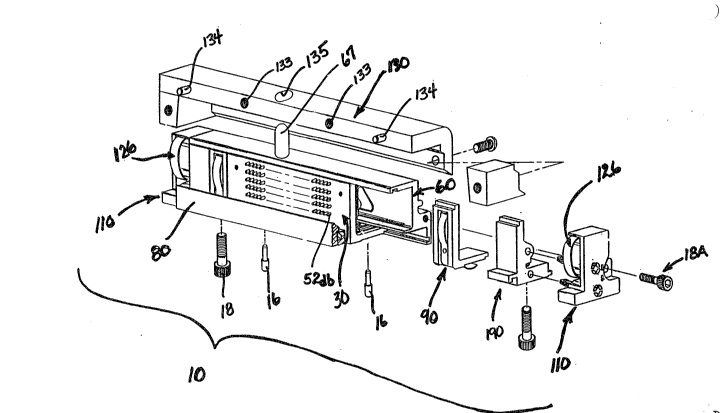
21 several views, there are shown in Figs. 2A, 2B partial e~ploded
- 22 perspectives of e~emplary embodiments of a modified_high densit~
23 backplane (MHD~) connector 10 according to the present invention
24 having utility for electrically interconnecting printed circuit
boards such aq a daughterboard 12 to a backplane or
- 14 -
.,:...
::,
. :
:
. . . .
..... :'. ~ .
.;
202~fi~8
1 motherhoard 14. The motherboard 14 and the daughterboard 12 each
2 include interconnect circuitry for electrically interconnecting
3 the printed circuit boards to the MHDB connector 10.
4 Partial plan views of representative motherboard and
daughterboard interconnect circuitry 20mb, , ~db are
6 illustrated in Figs. 16A, 17A. The motherboard interconnect
7 circuitry 20mb includes one or more geometric arrays 21mb f
8 signal/ground contact pads 23m~, discrete power contact
9 pads 22mb and discrete ground contact pads 2gmb as depicted
in Fig. 16A. The daughterboard interconnect circuitry 20db
11 consists of complementary geometric arrays 21db of
~ signal/ground contact pads 23db, discrete power contact
13 pads 22d~ and discrete ground contact pads 24db as depicted
14 in Fig. 17A.
As illustrated in Figs. 16B, 16C, 17B, 17C, the geometric
16 arrays 21mb, 21db consist of individual signal/ground contact
17 pads 23mb, 23db mounted in rows and columns to form
18 predetermined motherboard and daughterboard footprints. For the
19 motherboard geometric array 21mb, one of the outer ro~s of
contact pads are ground contact pads ~3mbG~ while for the
21 daughterboard geometric array 21db the top row of contact pads
æ are ground contact pads 23dbG.
. "
;; 23 Contact pad connection means 27mb, 27db electrically
:. 24 interconnect the signal/ground contact pads 23mb, 23db to the
. 25 motherboard and daughterboard, respectively. The motherboard 14
' ,`' ...
:- ~
.'..~`: ''
i . - 15 -
~, . ..
, " .
.`' .~' . .
'';'1
~":
~,
, . .
, ~
:
~ .
.
?
,~
02~6~
1 and daughterboard 12 have securing/alignment apertures 26S,
2 26a formed therethrough for aligning and securin~ the MHDB
3 connector 10 thereto, respectively.
4 The MHD~ connectors 10 e~emplarily illustrated in Figs. 2A,
2B include one or more contact modules 30,~ a connector
6 housing 60, a daughterboard biasing wedge 80, and connector end
7 caps 110. The MHDB connector 10 further includes a camming
8 member 130 configured to be secured to the daughterboard 12 and
9 to coact with the connector housing 60, a fle~ible film 140
interacting with elements of each contact module 30 (Fig. 10),
1l and a motherboard interactive biasing module 150 (Fig. 11) and a
12 daughterboard interactive biasing module 170 (Figs. 13A, 13B) for
13 each contact module 30. Depending upon the configuration and
. , . ~
` 14 application, the MHDB connector 10 may also include one or more
power contact modules 90 and one or more mounting blocks 190
. .
q 16 (Fig. 15) positioned intermediate and/or adjacent the e~ternal
17 ends of the contact modules 30.
, 18 Conversion or reconfiguration of the MHDB connector 10 for
.~ 19 different applications is facilitated by the addition or removal
of individual contact modules 30 as required. The embodiment
21 illustrated in Fig. 2A includes a single contact module 30 having
22 end positioned power modules 90 and mounting blocks 190. The
.
23 embodiment illustrated in Fig. 2B includes two spaced-apart
24 cQntact modules 30 -separated by intermediately positioned power
; 25 contact modules 90 and an intermediate mounting block 190.
:. .,"
,. ~
- 16 -
. . .
.. '. , .
.,, .:
' ::
~. :
: ',`` '~
~`~
2~2~8
1 For the e~emplary embodiments, each contact module 30
2 includes two hundred signal/ground contact elements 52db
3 defining a daughterboard array Sldb and two hundred
4 ground signal contact elements 52mb defining a motherboard
array 51mb (see Figs. lOA, lOB). Each exemplary array 51 is
6 arranged in five rows of forty contact elements 52 per row,
7 corresponding to the geometric arrays 21db, 21mb f
8 signal/ground contact pads 23db, 23mb of the daughterboard 12
9 and the motherboard 14, respectively (see Figs. 16, 17).
Accordingly, for the contact module 30 embodiments
11 e~emplarily illustrated in Figs. 2A, 2B, the MHDB connector la
12 may be incremented or decremented by two hundred signal/ground
13 contact elements 52 by adding or removing, respectively, one or
14 more contact modules 30. It will be appreciated that the contact
module 30 may ha~e other configurations, i.e., number of rows,
16 contacts per row, for the array of signal/ground contact
' 1
17 elements 52 depending upon the configuration of the interconnect
18 circuitry 20~b, 20db of the printed circuit boards to be
., . .;
19 electrically interfaced.
The contact module 30 of the present invention provides the
, "
21 means to align the MHDB connector 10 on the motherboard 14 and
. 22 holds the contact elements 52 that provide electrical
23 interconnection between the signal/ground contact pads 23mb,
:. _
; 24 23db of the motherboard 14 and the daughterboard 12 via the
'~ 25 flexible film 140. The contact module 30 is an integral element
.... .
~,:
..
- 17 -
:.. ` .. ..
''~ ;.
~"' . .
. ~ .
' ,
; ^ 2~2~6~8
1 formed from a nonconductive, high impact material, for e~ample,
2 plastics such as LCP ~liquid crystal polymer) or glass filled
3 eposies such as FR-4.
4 One embodiment of a contact module accordinq to the present
S invention is illustrated in Figs. 3A, 3~, 3C. Another embodiment
6 of a contact module according to the present invention is shown
7 in Figs. 3D, 3E~ 3F.
8 Referring to the drawings, the integral contact module 30
9 includes a first planar member 32 and a second planar member 4g
....
disposed to form a generally L-shaped configuration. The first
11 planar member 32 has a plurality of contact channels 34 formed
- ~ therein corresponding to the number of signal/ground contact
~i ~ pads 23db per row in the daughterboard geometric array 21db.
:.~ 14 A plurality of contact ports 36, corresponding ~o the number of
.i ~ rows of signal/ground contact pads 23db in the daughterboard
' '"A 16 geometric array 21db, are formed in each contact channel 34 to
...;:~ 17 extend through the planar member 32.
,
., 18 The planar member 32 also includes mounting bores 38. The
~ 19 mounting bores 38 of the embodiment of Figs. 3A, 3B, 3C are
:`~ 20 disposed in a cutaway portion 39 of the first planar member 32
21 while the mounting bores 38 of the embodiment of Fi~s. 3D, 3E, 3F
;.~ 22 are formed through the planar member 32 in a stepped
. . .
:.:. 23 coniguration. A first housing engaging shoulder 40 is formed in
24 the free end of the planar member 32 . A wedge engaging member 42
~?
;... 25 exte~ds outwardly from the planar mem~er 32 as illustrated in
. . .~
26 Figæ. 3C, 3F.
- 18 -
.. : .
:, ' ',
; .
...
''' '~''~ '
:` '~
, .~.,
... .
. -. . . ~.
.. ;
~` 202~8
1 The second planar member 44 includes alignment bores 46 for
2 aligning the contact module 30 for securement to the
. 3 motherboard 14, and a second housing engaging shoulder 50 formed
4 in the free end thereof. Each contact module 30 is aligned on
the motherboard 14 by alignment pins 16 (see Fig: 2), which are
6 fitted in alignment bores 46 of the planar member 44, that fit
7 into respective alignment bores 26a of the motherboard 14.
8 The planar member 44 of the contact module embodiment
. 9 illustrated in Flgs. 3A, 3B, 3C has a plurality of contact
channels 47 formed therein corresponding to the number of
11 signal/ground contact pads 23mb per row in the motherboard
~ geometric array 21m~. A plurality of contact receptacles 48
: ~ 13 are fo;med in each contact channel 47 to e~tend through the.~ 14 second planar member 44. For the embodiment of Figs. 3D, 3E, 3F,
.; 15 the plurality of contact receptacles 48 are formed through the
,.:
. ` 16 planar member 44 in a stepped configuration. The configuration
. 17 of the contact receptacles 4B correspond~ to the geometric
18 array 21mb of signal/ground contact pads 23mb f the
~.~ 19 motherboard 14.
:.;. 20 Esemplary contact elements 52db, 52m~ for the
;( 21 above-described contact modules 30 are depicted in Figs. 4A, 4B,
:,;
;-`. 22 respectively. The contact elements 52db, 52mb may be formed
23 as rivets having a head contact portion 5~ and a tail contact
... ?4 portion 56. The contact rivets 52db are configured for
~' 25 mounting and limited mo~ement within corresponding co~tact
;~ 26 channels 34 - contact ports 36 of the first planar member 32
. ~. .~.
...
.. . -- 19 --
..''`
.
;: .
`~ . .'
:
. .
~ .~ 202964~
1while the contact rivets 52mb are configured for mounting and
2limited movement within the corresponding contact channels 47 -
3contact receptacles 4~ or contact receptacles 48 of the second
.
4planar member 44, i.e., the contact rivets 52db, 52mb are
free floating. The contact rivets 52db, 52m~ held in the
6 first and second planar members 32, 44 form the first and second
7 contact arrays 51db, 51mb, respectively, of each contact
8 module 30. The contact rivets 52 are formed from a conductive
9 material, e.g., a copper alloy such as phosphor bronze.
10One embodiment of a connector housing of the MHDB
11 connector 10 is illustrated in Fi~. SA. Another embodiment of a
12 connector housing for the MHD~ connector 10 is shown in Fig. 5B.
~` 13 An alternative embodiment based on the configuration of the
14 connector housing illustrated in Fig. 5B is depicted in Fig. SC.
~ ~ The connector housing 60 is configured for assemblage with
: , 16 one or more contact modules 30 and is formed by conventional
, . . .
17 fabrication techniques, for e~ample, by e~trusion, as an integral
18unit from a material as aluminum (6061-T6) that may be finished
19 with teflon impregnated TUFRAM. The connector housing 60 is
readily formed to have any re~uired length, the required length
21 depending upon the number of contact modules 30 and other
22 components, e.g., power contact modules 90 and/or intermediate
,
`- 23 and/or end positioned mounting blocks 190 comprising the MHDB
24 connector 10. For the embodiment illustrated in Fig. 2A, the -
MHDB connector 10 has an o~erall assembled length of about ~.25
26lnches (about 108 mm3.
20 -
.
`:
; ' .
.
` ~` 2~2~6~8
The connector housing 60 includes a ~irst sidewall 62, a
second sidewall 64 generally parallel to and offset from the
3 first sidewall 62, and a top wall 66 integrallY e~tending from
4 the second sidewall 64. For the connector housing embodiment of
Fig. SA, a parti311y threaded circular channel 63 is formed in
6 the shoulder portion between the first and second
7 sidewalls 62, 64.
8 The connector housing 60 further includes a platform
9 member 68 e~tending outwardly from the shoulder portion between
.
'3 10 the first and second sidewalls 62, 6q. A first module engaging
~; 11 channel 70 is formed in the top wall 66 and configured for
engagement with the first housing engaging shoulder 40 of each
13 contact module 30. A second module engaging channel 71 is formed
in the second sidewall 62 and configured for engagement with the
second housing engaging shoulder 50 of each contact module 30.
1 16 A complementary camming structure 74 is integrally formed as
; 17 part of the connector housing 60 to project outwardly from the
;; 18 second sidewall 64. The complementary camming structure 74 is
:. 19 configured to interact with the camming member 130, which is
.~
.. 20 secured to the daughterboard 12, during mating of the
21 daughterboard 12 ~ith the MHDB connector 10. An alignment
. æ member 67 may be integrally formed with and depending outwardly
, 23 from the top wall 66. The alignment member 67 interacts with the
camming member 130 to align the daughterboard 12 fo~-- mating with
~ . .
~1 25 th~ MHDB connector 10~
;.
. , .
- 21 -
! .
` `' ' ' :
.~ ~
29648
1 With one or more contact modules 30 mounted on the
2 motherboard 14 as described hereinabove, the connector housing 60
3 may be mated with individual contact modules ~0 by sliding the
4 first and second module engaging channels 70, 71 onto the first
and second shoulders 90, 50, respectively, ~of the contact
6 module 30. With the connector housing 60 mated with the
7 individual contact modules 30, a first mounting chamber 72 for
~,j 8 the fle~ible film 140 and the daughterboard interactive biasing
9 module 170 is defined by one surface of the platform member 68,
the inner surfaces of the second sidewall 64 and the top wall 66
` 11 and a portion of the inner surface of the first planar member 32
in combination. A second mounting chamber 73 for the fle~ible
- 13 ilm 140 and the motherboard interactive biasing module lS0 is
14 similarly defined by the other surface of the platform member 68,
~ the inner surface of the first sidewall 62 and a portion of the
16 inner surface of the first planar member 32 and the inner surface
7 of the second planar member 44 in combination.
; 18 An alternative embodiment based upon the configuration of
19 the connector housing 60 illustrated in Fig. 5B is shown in
;; 20 Fig. 5C. In addition to the structural features described in the
-~ 21 preceding paragraphs, the connector housing 60' further includes
22 a partial cylindrical channel 76 terminating in first and second
23 surfaces 77, 78, respecti~ely. A locking rod (not shown),
24 operative in combination with the connector end caps 110, may be
disposed within the partial cylindrical channel 76 to lock the
26 connector housing 60 into final position in the MHDB connector 10
27 assemblage.
~ - 2Z -
: ~ `
", :
; .:.................................... ~
, ~
2~29~48
: `
1 Exemplary embodiments of daughterboard biasing wedges 80
2 according to the present invention are depicted in Figs. 6A~ 6B.
3 The biasing wedge 80 is formed, for e~ample, by e~trusion, as an
4 integral unit from a material such as aluminum (6061-T6~ or
tic. The biasing wedge 80 is readily formed in any
6 convenient length, depending upon the number of contact
7 modules 30 in the MHDB connector 10.
` ~ The biasing wedge 80 has a generally L-shaped configuration
9 and includes a complementary contact module engaging portion 82,
an insertion surface 84, and a daughterboard engaging
11 surface 86. The biasing wedge 80 may be mated to the contact
12 modules 30 by sliding the complementary contact module engaging
13 portion 82 into the wedge engaging member 42 of the contact
14 module 30. During mating of the daughterboard 12 with the MHDB
connector 10, tbe edge of the daughterboard 12 moves along the
16 insertion surface 82, thereby ensuring that the daugh~erboard 12
~h 17 is properly aligned for mating.
With the daughterboard 12 mated to the MHDB connector 10,
1~ the daughterboard 12 is mechanically engaged by the opposed,
.20 spaced-apart engaging surfaces 86 of the wedge 80. This
~ ~1 mechanical engagement prevents the daughterboard 12 from creeping
- ~ or ~walking~ away from the MHDB connector 10. The biasing
wedge 80 ensures that a positive electrical interzonnection is
!4 maintained between the- interconnect circuitry 20d~ of the
~ daughterboard 12 and the corresponding contact elements o the
6 contact modules 30.
- 23 -
. . ..
:
' ` ,
.' ,' ' ~
2~296~8
1 An e~emplary power contact module 90 for the MHDB
` 2 connector 10 of the present invention is e~emplarily illustrated
. 3 in Figs. 7A-7D. The power contact module 90 includes a power
4 contact module clip 92 (Figs. 7A, 7B) and a resilient power
contact 105 (Figs. 7C, 7D). The power contact modules 90 may
6 provide both supply and return contacts and can be added or
7 removed from the MHDB connector 10 as required, depending upon
the particular application and the number of contact modules 30.
9 The power contact module clip 92 is integrally formed from a
nonconductive material such as plastic, e.g., LCP, and has a
11 gPnerally L-shaped configuration. The power contact module
12 clip 92 has housing engaging shoulders 94, 94 formed at the free
13 ends thereof configured to mechanically engage the first and
14 second module engaging channels 70, 71 of the connector
~ 15 housing 60.
;~ 16 The power contact module clip 92 also has first and second
17 contact windows 96, 98 formed therein. The first and second
18 contact windows 96, 98 are separated by a transverse member 100.
lY Contact retention slots 102 are formed in the module clip 92
superjacent the transverse member 100. A pin 104 is formed to
~1 depend outwardly from the transverse member 100 as illustrated.
2~ The power contact 105 is formed from a conductive material
Z3 such as a copper alloy, e.g., No. C172, and has a resilient
~4 configuration adapted for mating with the module clip 92. The
power contact 105 includes opposed detents 106, a complementary
26 pin hole 107, a daughterboard engagingsegment 1~8, and a
~7 motherboard engaging segment 109.
'''~'
, - 24 -
.
.
. :
.: . :
.
6 ~ 8
~ 1
The opposed detents 106 are configured for insertion within
.~ ~ the contact retention slots 102. The module clip 92 and power
.` 3 contact 105 are positioned for assemblage in the MHDB
:
: 4 connector 10 by inserting the pin 104 through the complementary
~ pin hole 107.
6The daughterboard engaging segment 108 is positioned in the
7 first contact window 96 and protrudes outwardly therefrom. The
: 8 daughterboard engaging segment 108 is positioned to mechanically
. 9 and electrically resiliently engage a corresponding discrete
power contact pad 22db f the daughterboard geometric
. 11 array 21db. The resilient interaction between the the
. ~ daughterboard engaging segment 108 and the corresponding discrete
~ power contact pad 22db e~erts a biasing force against the
14 daughterboard 12 to effect sequenced mating of the
j ~ daughterboard 12 with the MHDB connector 10.
~,.~,,
The motherboard engagin~ segment 109 is positioned in the
. 17 second contact window 98 and protrudes out~ardly therefrom. The
; 18 motherboard engaging segment 109 is positioned to mechanically
19 and electrically resiliently engage a corresponding power contact
pad 22mb f the motherboard geometric array 21mb.
. ~1 Various embodiments of connector end caps 110 according to
22 the present inve~tion are e~emplarily illustrated in Figs. 2A, 2B
23 and shown in greater detail in Figs. 8A-8L. The connector end
.,
' 24 - caps 110 provide a means for sealing the exposed ends of the MHDB
.~' 25 connector 10. The connector end caps 110 may also provide a
26 means for localized secureme~t of the MHDB connector 10 to the
, , .
- 25 -
. . ~ .
i'`:` -: ,. ..
, :
. ~.
~;
:
:
.~ ,~ . , , ' " .
:'` ' ' ' ' ~ '',' ' ''
.
.
:
` - 2~2~
1 motherboard 14 ~see embodiment of Fig. 8E). The connector end
. . .
2 caps 110 may be integrally formed from a rigid material such as
3 plastic, e.g., LCP, by any of the various fabrication techniques,
4 such as molding.
One embodiment of the connector end cap 110 is illustrated
6 in Figs. 8A, 8B, 8C. This particular embodiment is configured
7 for utilization in combination with end positioned mounting
8 blocks 190 as illustrated in Fig. 2A. The connector end cap 110
9 includes an end cap member 112 configured to receive an early
mate resilient ground contact 126 in combination therewith. The
; 11 ground contact 126 for the embodiment of Figs. 8A-8C is
, ,
12 illustrated in Figs. 8I, 8J. The resilient ground contact 126,
13 which may be formed by stamping from a conductive material such
14 as a copper alloy, includes a motherboard engaging portion 127, a
daughterboard engaging portion 128 and an end cap engaging
16 means 129. For this particular embodiment, the end cap engaging
17 means 129 comprises a pair of spaced-apart detents.
18 The end cap member 112 of this embodiment includes contact
l9 positioning portions 113, contact retention means 114, in this
embodiment a pair of spaced-apart detent slots, a securement
21 bore 115, one or more segmented engagement prongs 116 and a
22 sealing portion 117. The resilient ground contact 126 is mounted
23 in combination with the end cap member 112 by snap engaging the
24 detents 129 into- the contact detent slots il4 with the
2~ daughterboard engaging portion 128 of the contact 126 positioned
. ~ i
;~ 26 adjacent the outer surface o the intermediate contact
27 po~itioning portion 113i.
,.~
i~ - 2~ -
' ''`
: `
, ',, .. ~ . . .
, .' , .
- - - -
2~29648
1 The segmented engagement prongs 116 are configured for snap
2 engagement within stepped bores 197 of the abutting mounting
3 block 190 as illustrated in Fig. 2A. Securement screws 18A are
4 inserted through the securement bores llS of the connector end
caps 110 and threadingly engaged in the threaded circular
6 channels 63 of the connector housing 60 during final assemblage
7 of the MHDB connector 10. The sealing portion 117 of the end cap
8 member 112 engages the wedge engaging member 194 of the abutting
9 mounting block 190 to retain the contact modules 30, the
daughterboard biasing wedge 80, the power contact modules 90 and
11 the mounting blocks 190 in static fi~ed relation with respect to
12 one another.
13 With the MHDB connector 10 secured to the motherboard 19,
14 the motherboard engaging portions 127 of the resilient ground
contacts 126 of the connector end caps 110 are biased into
16 engagement with respective discrete ground contact pads 24mb f
17 the motherboard 14. ~uring mating, the daughterboard engaging
18 portions 128 of the resilient ground contacts 126 initially coact
19 with the daughterboard 12 to exert biasing forces thereagainst to
provide sequenced mating thereof with the MHDB connector 10. The
21 daughterboard en~aging portions 128 of the ground contacts 126
22 engage the daughterboard discrete ground pads 24db during the
23 mating sequence to provide an early ground interconnect between
24 the motherboard 14 and the daughterboard 12. --
... i .
:`'`',
~ . 27 _
. .
:.
`
,
~ ` " 20296~8
1 Another embodiment of connector end caps 110 according to
2 the present invention are illustrated in Figs. 8D, 8E. Th;s
3 particular embodiment may be utilized without the end positioned
4 mounting blocks. The end cap member 112 of this embodiment is
S configured to recei~e the early mate resilient ground contact 126
6 depicted in Figs. 8R, 8L. The end cap engaging means 129 for
7 this ground contact 126 is a mating bore formed through the
8 central portion thereof.
9 The end cap member 112 includes contact positioning
portions 113, contact retention means 114, in this embodiment a
11 threaded bore and corresponding retention screw (not shown), a
12 securement bore 115 and a sealing portion 117. The end cap
13 member 112 further includes a housing engagement portion 120
14 integrally formed therewith. The housing engagement portion 120
includes housing engaging shoulders 121 configured for slîding
16 engagement into the first and second module engaging
17 channels 70, 71 of the connector housing 60, a wedge engaging
18 shoulder 122, and upper and lower abutment segments l23, 124.
19 The resilient ground contact 126 is mounted in engagement
with the end cap member 112 by inserting the retention screw
21 through the retention bore 129 and into the threaded bore 114
22 formed through the intermediate contact positioning
23 portion 113i. The daughterboard engaging portion 128 is spaced
24 apart rom the upper contact positioning-portion 113U.
.,
- 28 -
., '' ' ..
. ~ . .
_
,
;;
.~ . .
.
` ~` 2~2~i4~
1 The connector end caps 110 are secured to the connector
2 housing 60 by sliding the engaging shoulders 121 and the wedge
.::. 3 engaging shoulder 122 into the first and seco~d module engaging
: 4 channels 70, 71 of the connector housing 60 and the complementary
module engaging member 82 of the daughterboard biasing wedge 80,
. 6 respectively. Securement screws 18A are inserted through the
7 securement bores 115 into threaded engagement circular
8 channels 63 of the connector housing 60. The housing engagement
; 9 portion 120 abuttingly engages engages the daughterboard biasing
wedge 80 and the power contact modules 90 or the contact
11 modules 30 to maintain same in static fi~d relation with respect
12 to one another. The upper and lower abutment segments 123, 124
13 of the connector end caps 110 of this embodiment engage
: 14 corresponding ends of the daughterboard interactive biasing
: 15 module 170 and the motherboard interactive biasing module 150,
....
16 respectively, thereby ensuring that the modules are maintained in
17 proper orientation within the contact modules 30.
18 Still another embodiment of a connector end cap member 110
19 according to the present in~ention is illustrated in Figs. 8F,
8G. The end cap member 112 of this embodiment is configured to
21 receive an early mate resilient ground contact 126 similar to the
22 one depicted in Figs. 8X, 8L. The ground contact 126 for use in
23 combination with this connector end cap member 110 need not have
24 a mating bore 129 formed therethrough.
,
. '
.':' ' :.
.. ~ . .
',`. ,~ ~ - .:
` ~ 2029~4~
::
;: 1 The end cap member 112 includes contact positioning
2 portions 113 and contact retention means 11~, in this embodiment
: 3 a contact channel dimensioned to frictionally engage the
4 intermediate portion of the resilient ground contact 126. The
end cap member 112 further includes a housing engagement
6 portion 120 ha~ing housing engaging shoulders 121 and upper and
:7 lower abutment segments 123, 124. ~ securement bore 115 is
8 formed through the lower abutment segment 124.
9 The resilient ground contact 126 is mounted in engagement
with the end cap member 112 by insertin~ the intermediate portion
11 thereof into contact channel 114. The free end of the
12 daughterboard enqaging portion 128 is positioned opposite the
13 upper contact positioning portion 113U. The connector end
14 caps 110 are secured to the connector housing 60 by sliding the
engaging shoulders 121 into the first and second module engaging
:~ 16 channels 70, 71 of the connector housing 60. Securement
' 17 screws 18 are inserted through from the underside of the
18 motherboard 14 and threaded into the securement bores 115 such
19 that this particular embodiment provides localized securement to
the motherboard 14. The housing engagement portion 120
21 abuttingly engages the power contact modules 90 or the contact
; 22 modules 30 to maintain same in static fi~ed relation with respect
23 to one another. The upper and lower abutment segments 123, 124
:. 24 of the connector end caps~-~~llO o~ this embodiment engage
corresponding ends of the daughterboard interactive biasing
~. .
~ - 30 -
',
.', ' - ;
~; ~
20296A8
.
module 170 and the motherboard interactive biasing module 150,
2 respectively, thereby ensuring that the modules are maintained in
3 proper orientation within the contact modules 30.
Another embodiment of a connector end cap 110 is illustrated
in Fig. 8H. This embodiment includes two end cap members 112a,
6 112b having configurations suitable for assemblage with the other
elements of the connector, e.g., contact modules 30, connector
8 housing 60, power contact modules 90 and/or mounting blocks 190.
g This embodiment includes a camming means 119 that comprises a
' 10 cammi~g linkage. The camming linkage 119 interacts with the
.~ 11 daughterboard 12 to bias the daughterboard 12 into adjacency with
12 the contact modules 30. This embodiment of the connector end
13 cap 110 eliminates the need for camming coaction between the
14 camming member 130 and the connector housing 60 such that the
;~ lS struc~ures thereof may be simplified.
'`; 16 Camming members 130 according to the present invention are
esemplarily illustrated in Figs. 2A and 9A, 9B. The camming
..:,
18 member 130 is configured to coact with the connector housing 60
19 f the present invention to provide a positive means for
sequencing movement, during mating, of the complementary
21 signal/ground contact pads 23db f the daughterboard 12 into
22 contact with the arrays 51db o~ contact rivets 52db disposed
` in the first planar member 32 of the contact module 30, thereby
~ 24- facilitating con~act wipe thereof. The camming member 130 also
.~ 25 provides proper alignment between the daughterboard 12 and the
: 26 MHD~ connector 10. The camming mem~er 130 is formed as an
'' .
; - 31 _
. :',
`'`'
: .
; ~, ~ ' '
t
~` 202~8
1 integral member, for e~ample by extrusion, from a structùrally
2 rigid material such as aluminum (6061-T63 or plastic and is
3 readily formed in any convenient length, depending upon the
4 number of contact modules 30, power modules 90 and/or mounting
5 blocks 190 comprising the MHD~ connector 10.
6 The camming member 130 includes a securing segment 132 and a
7 camming segment 136. The securing segment 132 has threaded
8 bores 133 formed in the end face thereof. Securing screws 17 are
9 inserted through securing bores 26S in the daughterboard 12 and
into the threaded bores 133 to rigidly secure the camming
11 member 130 to the daughterboard 12. The securing segment 132 may
12 include alignment pins 134 to facilitate aligning the camming
; 13 member 130 for securement with the daughterboard 12. The
: 14 securing segment also includes a keying channel 135 configured to
: . 15 recei~e the alignment member 67 of the connector housing 60 to
.. 16 align the daughterboard 12 for mating with the MHDB connector 10.
~ 17 The camming segment 136 is configured for camming and
.~j 18 engaging coaction with the connector housing 60. The internal
1~ surface of the camming segment 136 includes first and second
i 20 tapered camming surfaces 137a, 137b and first and second planar
21 engaging surfaces 138a, 138b. During mating the first and second
22 tapered camming surfaces 137a, 137b coact with camming member 74
~ ,
.. 23 and the upper edge of the connector housing 60, respectively, to
24 bias the daughterboard signal/ground contact pads 23db into
corresponding elements of the daughterboard array 51db of
. 26 contact ri~ets 52d~. The first and s~cond planar engaging
- 32 -
,
.
' ~. . ' ' ~ '
-.
~02~
1surfaces 138a, 138b mechanicallY engage the camming member 74 and
2 the connector housing 6U to complete the mating sequence. The
3 embodiment of Fig. 9A further includes a recess 139 for nesting
4 of the camming member 74.
5The fle~ible film 140 embodiments e~emplarily illustrated in
6 Figs. lOA, lOB, lOC are fabricated from a resilient dielectric
7 material. Heat-resistant polymers such as polyimides are a
8 representative dielectric having excellent electrical properties
9 and which are readily formable into thin, bendable fle~ible
~ 10 films. A preferred embodiment of the flexible film 190 is
;~ 11 d~picted in Figs. lOA, 10~. The preerred embodiment e~emplarily
12 illustrated has a width of about 1.04 inches and a length of
~ 13 about 2.50 inches. Fig. lOC illustrates an alternative
; 14 embodiment of the flexible film 140 according to the present
- 15 invention.
16The flexible film 193 has registration holes 141 formed
17thr~ugh the ends thereof to facilitate registration with the
!
; 18corresponding contact module 30. A conductive matri~ 142 is
; lg formed on one major surface of the fle~ible film 190 and includes
` 20 first and second spaced-apart arrays of contact pads 143
21 electrically interconnected by a plurality of conductive
22traces 14~. The esemplarily illustrated conductive traces 144
23 have widths of about 0.005 inches and interspacings of about
., 24 a.oos inches. The finished conductive~matri~ 142 will have an
impedance of about 50 ohms.
. .
. '''` .
~ 33 -
''`' ' . ........ .
.. . .
'.~:' ,, ,:
:. .
.
~``: ' ,
... .
0296~g
1Metallic ground strips 146 are formed along opposite
2longitudinal edges of the flexible film 140 embodiment
3illustrated in Fig. lOA. Each metallic ground strip 146 includes
~, 4a plurality of plated-through holes 147. The conductive
5matri3 142 and the metallic ground strips 146 are formed from
6electrically conductive material such as electrolytic plated
7copper by conventional photolithographic techniques.
8A conductive ground plane 148 is formed on the other major
, 9surface of the fle~ible film 190 as illustrated in Fig. lOB. The
plurality of plated-through holes 147 pro~ide the electrical
11interconnection between the conductive ground plane 148 and the
12conductive ground strips 146. The ground plane 148 is formed
from electrically conductive material such as electrolytic plated
14copper by conventio~al plating techniques.
.
~5An alternative embodiment of the fle~ible film 140 according
, 1~ to the present invention is illustrated in Fig. lOC. The
17 embodiment of Fig. lOC is similar to the embodiment of Figs. lOA,
8 lOB but does not include conductive ground strips and the
1~ plurality of plated-through holes. Also, the arrays of
: 20 conductive pads 143 comprise five rows of contact pads whereas
21 the arrays of conductive pads 143 of the embodiment of Figs. lOA,
:~ 22 lOB comprises four row~ of co~tact pads.
~;' 23The conductive matri~ 142 provides the electrical
24 interconnect between the signal~ground contact pads 23mb,
23db of the motherboard 14 and daughterboard 12, respectively,
, 26 via the contacts 52 of the contact module 30. The geometric
- 34 -
...
.
:~`
: .. , . . ::
:.
: ', ' ', ~ . ~
202~g
~ pattern of the conducti~e matri~ 142 corresponds to the contact
arrays 51mb, 51db of the contact modules 30 as described
3 hereinabove. For the embodiment of Fig. lOA, the four rows of
4 contact pads of the arrays 143 electricallY interface with the
signal contact elements 52 of the contact modules 30. The ground
, 6 strips 146 electrically interface with the ground contact
i~
i 7 elements 52 of the contact modules ~0. For the embodiment of
8 Fig. lOC, the outermost rows, i.e., those pro~imal the
9 longitudinal edge, of contact pads of the arrays 143 electrically
iO interface with ground contact elements 52 of the contact
11 modules 30.
12 An e~emplary motherboard interactive biasing module 150 and
: .
13 an exemplary daughterboard interactive biasing module 170
14 according to the present invention are illustrated in Figs. 11
and 13A, 13B, respectively. The interactive biasing modules 150,
16 170 provide uniform contact force distribution between the
17 fle~ible film 140 and the first and second arrays Slmb, 51db
18 of contact rivets 52, respectively. The interactive biasi~g
19 modules 150, 170 also provide displacement tolerance relief for
2~ the first and second arrays 51mb, 51db of contact rivets 52
21 disposed in each contact module 30, respectively.
~2 The motherboard biasing module 150 includes a resilient
23 pad 152, a distribution plate 15q and a motherboard force
24 generating spring 156. The resilient pad 152 is formed from a
~5 elastomerîc material such as silicone rubber that provides
26 point-to-point compression variances. The resilient pad 152
~'
- ~5 -
'` l~
.. .
. .,
.~``,
~',''~
.~ . . ..
.. . .
. : , .
., . : , .
~: 2029648
1 abuts the ground plane side of the fle~ible film 140 and provides
2 displacement tolerance relief for the corresponding
3contacts 52mb of the contact module 30. The resilient pad 152
4abuts the distribution plate 154. The distribution plate 154 is
.. 5 formed from a structurally rigid material such as stainless steel
6(type 302-304), aluminum or high impact plastic and provides an
7even distribution of the biasing force generated by the
8motherboard force generating spring 156 over the respective
~interconnect regions.
10Several e~emplary embodiments of the motherboard biasing
11 spring 1S6 according to the present invention are illustrated in
1~Figs. 12A, 12B, 12C, 12D and 12E, 12F, 12G. The motherboard
13 biasing spring 156 is a structure formed from a resilient
. .
14 material such as stainless steel (carpenter custom 455) that
1~ provides the force to bias the fle~ible film 190 into mechanical
16 and electrical engagement with the contacts 52. The motherboard
17force generating spring 156 includes mounting tabs 157 having
lh holes 158 formed therethrough for securing the spring 156 to the
19distribution plate 154. The force generating spring 156
~embodiment of Fig~. 12A, 12B, 12C, 12D comprises a plurality of
21alternating curved leaves 160 having end portions 159. The force
22generating spring 156 embodiment of Figs. 12E, 12F, 12G comprises
~3 spaced-apart elongated curved segments having end portions 159.
24 - The end portions 159 mechanically engage the platform member 68
to provide the biasing force thereof.
.
. .
- 36 -
:,
.' ~`
.
'"' ' ''. '
~ i
`,': " ' '
. "
202~4~
.
. 1 One embodiment of a daughterboard interacti~e biasing
:i 2 module 170 according to the present invention is illustrated in
3 Fig. 13A. The biasing module 170 includes a resilient pad 172, a
4 distribution plate 174 and a daughterboard force generating
spring 176. The resilient pad 172 is formed from a elastomeric
: 6 material such silicone rubber that provides point~to-point
7 compression variances. The resilient pad 172 abuts the ground
~ plane side of the fle~ible film 140 and provides displacement
; 9 tolerance relief for the corresponding contacts 52db of the
contact module 30. The resilient pad 172 abuts the distribution
~ plate 17~. The distribution plate 179 is formed from a
12 structurally rigid material such as stainless steel (type
13 302-304), aluminum or high impact plastic and provides an even
: 14 distribution of the biasing force generated by the daughterboard
force generating spring 176 over the interconnect region.
16 Another embodiment of the daughterboard interactive biasing
, 17 module 170 is illustrated in Fig. 13B. The interactive biasing
1~ module 170 is as described hereinabove and further includes an
19 adjustment plate 184 and an adjusting means 186. The adjustment
plate 184 is formed from a structurally rigid material such as
~1 stainless steel (type 302-304), aluminum or high impact plastic
2~ and is configured to retain the end portions 182 of the
23 daughterboard force generating spring 176. The adjustment
. ~4 plate 184 abuts against the second- sidewall 64. The adjusting
means 186 illustrated is a set screw disposed through the
.. connector housing 60 to mechanically engage the adjustment
:~ - 37 -
. I
~: ..... . .
: ,
.
:!
-:
. ,~
.
;'' . '
-~20296~
plate 184. The adjustment plate 184 and the adjustment mea~s 186
in combination provides a means of ad~usting the biasing force
3 exerted in the contact region to compensate for variations in
4 tolerances in manufacturing and mating.
Several e~emplary embodiments of the daughterboard force
6 generating spring 176 are depicted in Figs. 14A, 14B, 14C, 14D
7 and 14E, l9F, 14G. The daughterboard force generating spring 176
8 is a discontinuous structure formed from a resilient material
9 such as stainless steel (carpenter custom 455) that provides the
force to bias the fle~ible film 140 into mechanical and
11 electrical engagement with the contacts 52. The daughterboard
~2 force generating spring 1~6 includes mounting tabs 177 having
13 holes 178 formed therethrough for securing the spring 17~ to the
14 distribution plate 174. The force generating spring 176 includes
a plurality of alternating cur~ed leaves 180 having end
16 portions 182 which mechanically engage the second sidewall 64 or
17 the adjustment plate 184 to provide the biasing force thereof.
18 Various embodiments of mounting blocks 190 according to the
19 present invention are e~emplarily illustrated in Fiqs. 2A, 2B and
Figs. 15A, 15B, 15C. The mounting block 190 may be integrally
21 formed from a rigid material such as aluminum ~6061-T6~, which
æ may be finished with teflon impregnated TUFR~M, or high impact
23 plastic by any of the various fabrication techniques, such as
24 e~trusion, and is readily formed to a predetermined
configuration. The mounting blocks 190 may be used as an
26 intermediate spacin~/securing element (Fig. 15C) or may be used
- 38 -
.. . ..
. .
''`'``
':~
. . .
',~' ' :'
.. .
. ~ -
. . .
02~4~
1 as an end positioned securing element (Figs. 15A, 15B) in
2 combination ~ith connector end caps 110. Fig. 2A illustrates the
; 3 latter use while Fig. 2~ illustrates the use of the mounting
4 block 190 as an intermediate spacing means and as a means for
securing the MHDB connector 10 to the motherboard li.
6 The intermediate mounting block 190 includes housing
~ engaging shoulders 192 configured for sliding engagement with the
8 first and secon~ module engaging channels 70, 71 of the connector
9 housing 60, a wedge engaging member 194 configured to engage the
complementary contact module engaging member 82 and abutment
11 surfaces l9S, 196 to engage abutting elements comprising the MHDB
; 12 connector 10, e.g., contact modules 30, power contact
13 modules 90. The mounting block 190 has a mounting bore 198
14 formed therethrough and configured to receive a securing screw 18
` 15 inserted through securing hole 26S to fasten the mounting
16 block 190 to the motherboard 14.
. 1/ The embodiments illustrated in Figs. 15A, lSB further
: . 18 include stepped bores 197. The stepped bores 197 are eonfigured
~; 19 for snap-engagement reception of the segmented engagement
2U prongs 116 of the connector end caps 110. The embodiment o~
` , 21 Fig. 15C may be utilized in combination with a resilient spring,
. ...
.~ ~2 similar to that illustrated in Figs. 8~, 8L. The resilient
2~ spring coacts with the daughterboard 12 to e~ert a supplemental
24 biasing- force thereagainst or sequenced mating of the
daughterboard 12 to the MHDB connector 10.
. . .
.l - 39 -
. ,,.~
,'
`~
; .
.
.... ; .
:,
,:
2029~48
E~emplarily, the MHDB connector 10 is assembled in
combination with the motherboard 14 by first aligning each
~ contact module 30, preloaded with the arrays Slmb, 51db of
4 rivet contacts 52, thereon by inserting alignment pins 16 that
are fitted into the alignment bores 46 of each contact module 30
through holes 26a on the motherboard 14. The fle~ible film 140
7 is disposed in registration with each contact module ~0 and the
; ~ motherboard and daughterboard interactive biasing modules 150,
9 170 disposed in combination with each contact module 30.
The connector housing 60 is assembled in combination with
11 the contact module 30 by sliding the first and second module
lZ engaging shoulders 70, 71 onto the corresponding shoulders 90, 50
;13 of each contact module 30. Power contact modules 90, as
14 required, may be assembled in combination with the connector
housing 60 by sliding the housing engaging shoulders 94 of each
l6 module 90 into the corresponding first and second module engaging
~'7 channels 70, 71 of the housing 60. Mounting blocks 190, if
..8 utilized as intermediate spacing/securing elements, may be
.9 assembled in combination with the connector housing 60 by sl;ding
~'0 the housing engaging shoulders 192 of each block 190 into the
1 corresponding first and second module engaging channels 70, 71 of
2 the housing 60.
The daughterboard biasing wedge S0 is assembled in
combination with the connector by sliding the complementary
~i contact module engaging portion 82 into the wedge engaging
member 42 of the contact module 30 and the wedge engaging
' member 194 of any ~ntermediate mounting blocks 190.
. ., ~
, :. .
~ _ 40 _ . .
~ . , .
' ''
....
.: .
'. ' ' ., :
. . ~: .
2029648
1The MHDB connector 10 is sealed by mating the connector end
2 caps 110 to aforedescribed assemblage. ~nd positioned mounting
3 blocks 190 may be utilized as required by the particular
4 connector end cap 110 configuration. The MHDB connector 10 is
secured to the motherboard 14 by inserting securing scr2ws 18
6 through the motherboard 14 into the securement bores 115 o the
7connector end caps 110 or the mounting bores 198 of end
positioned mounting blocks 190.
9With the MHDB connector 10 assembled as discussed
hereinabove, each motherboard interactive biasing module 150
11 e~erts a biasing force against the corresponding region of the
12 respective fle~ible film 140 to bias the array 1~3 of contact
13 pads thereof into mechanical and electrical engagement with
14 corresponding array 51mb of riYet contacts 52mb. Each rivet
contact 52mb is thereby biased into mechanical and electrical
16 engagement with a corresponding motherboard signal/ground contact
17 pad 23mb. As illustrated in Fig. 16C, each rivet
18 contact 52mb engages the corresponding motherboard
~ signal/ground contact pad 23mb at a defined contact zone 28mb.
20Ma~ing of the daughterboard 12 (with the camming member 130
~1 secured thereto~ is effected br pressing the daughterboard 12
2~ downwardly onto the MHDB connector 10. The resilient ground
23 contacts 126 of the connector end caps, and the resilient spring
~4 of any intermediate mounting blocks 190, initially interact with
2~ the daughterboard 12 to bias the daughterboard 12 away from the
26 MHDB connector 10, thereby preventing premature engagement of the
.... ,` .
~ - 41 -
. 1 .
' '
. .
.~ ~
'`'
.
-
2029648
1 daughterboard signal/ground contact pads 23db with the2 array 51db of contact rivets 52db of corresponding contact
3 modules 30. The resilient ground contacts 126 also provide early
4 mating between the discrete ground pads 24mb of the
motherboard 14 and the discrete ground pads~24db of the
6 daughterboard 12. As the daughterhoard 12 is progressively mo~ed
/ downwardly into the MHD8 connector 10, each resilient power
8 contact 105 interacts with the daughterboard 12 to supplement the
9 ~away from~ biasing force provided by the resilient ground
contacts 126.
11 Further downward displacement of the daughterboard 12 causes
12 a coaction between the complementary camming structure 74 and the
13 connector housing 60 and the tapered camming surfaces 137a, 137b,
14 respectively, of the camming segment 136 of the camming
member 130. The camming coaction is sufficient to overcome the
16 biasing forces e~erted by the resilient elements, thereby
17 displacing the daughterboard 12 into the MHDB connector 10. This
18 camming coaction also prevents relative rotational movement
19 between the daughterboard 12 and the MHDB connector 10. The
2~ displacement causes the daughterboard signal/ground contact
21 pads 23db to initially engage corresponding elements of the
~2 array 51db of ri~et contacts 52db at an initial contact
23 zone 28dbi, as illustrated in Fig. 17C.
24 A final very - small downward -displacement of the
daughterboard 1~ completes the mat;ng process. The small
26 downward displacement cause~ each rivet contact 52db to
27 translate along th~ surface of the corresponding daughterboard
. - ~2 - .
..`''`
,, . :
. . ~
... . .
. ... .
.. -~ '.~ .
202~6~8
` .
1 contact pad 23db to a final contact ~one 28dbf~ as
2 illustrated in Fig. 17C. The translation of each rivet
3 contact 52db between the initial contact zone 28dbi and the
4 final contact zone 28db~ provides the wiping action that
ensures good electrical interconnection between the respective
6 contact elements.
7 In the mated state, the leading edge of the daughterboard 12
~ is engaged with daughterboard engaging surface 86 of the biasing
9 wedge 80. Concomitantly, the planar engaging surfaces 138a, 138b
1~ (and/or the recess 139) mechanically engage the connector
11 housing 60. These engagements prevent the daughterboard 12 from
~; 12 creeping away from the MHDB connector 10, thereby ensuring a
1~ positive electrical interconnection therebetween.
, .;
: ~ 14 The MHDB connector of the present invention provides the
capability of electrically interconnecting printed circuit boards
1~ having a high density of input/output contact interconnects. The
1 17 modular elements of the MHDB connector are of relatiYely
-~ 18 straightforward design, thereby facilitating the ease and co~t nf
i 1~ manufacturing by conventional methods. The MHDB connector is
' 20 independent of printed circuit board thicknesses and variations
"~ in tolerances. Moreover, the modular elements are easily
-1 2~ resized, reconfigured, and/or interchanged to facilitate use
23 thsreo with printed circuit boards of varying dimensions and/or
~4 varying contact pad densities. ~~~
.,
.. .
,
~ - 4~ _
' '
;`'
;'~
:: :
.:':~, .
: ,-
:
20~64~
The MHDB connector of the present invention does not require
a separate and/or complex camming mechanism. The camming
3 elements of the MHD~ connector are readily formed as integral
4 element~ of the connector housing or the connector end caps. The
camming elements of the MHD~ connector provide a wiping action
6 between interconnecting conducti~e elements, provide a sequential
7 mating capability, and re~uire only a low ins~rtion force to
8 effect mating between printed circuit boards. The inherent
9 simplicity and operation of the camming elements greatly
increases the reliability of the MHDB connector.
11 Each contact module is assembled with preloaded rivet
1~ contacts and readily assembled in combination with the fle~ible
13 film and the corresponding interactive biasing modules, thereby
14 facilitating assemblage thereof. The preloaded ri~et contacts
are free-floating and coact orthogonally with the contact
16 interconnects formed on the fle~ible film. Orthogonal coaction
substantially `eliminate~ the possibility of any erosion and/or
18 abrasion damage of the contact intercvnnects of the fle~ible
19 film, thereby maintaining signal path integrity and impedance
. . .
~ 2~ matching. The conductive matri~ and the ground plane are readily
:.. 21 formed as continuous circuit paths on the fle~ible film to ensure
~2 precise impedance matching for printed circuit board
; 2~ interconnect~, These features provide enhanced electrical
.1 24 per~ormance f~r the MHDB connector.
. ~
.
~ ~!
, - q4 -
'.
.'', ` .
;`'''
:.
,
'
2~2~6~
1 A variety of modifications and variations of the present
2 invention are possible in light of the above teachings. For
3 example, the connec~or end cap configuration may include an upper
4 cap member tha~ is secured to the camming member mounted to the
daughterboard and which interfaces with the upper surface o~ the
6 connector end cap as illustrated in Fig. 2A. Alternatively, the
/ upper cap member may include a pin member that is inserted into a
. 8 corresponding hole in the camming member.
9 Alternatively, the daughterboard biasing wedge 80 as
- 10 described hereinabove may be replaced by the daughterboard
. 11 camming subassemblies 200 e~emplarily illustrated in Figs. l~A,
.. ~ 12 18B. The daughterboard camming subassemblies 200 include
means 202 for mechanically engaqing the wedge engaging member 42
~, 14 of the contact module 30 and means 204 for displacing the
.`, 15 daughterboard 12 înto the contact module 30. For the embodiment
` i6 of Fig. 18A, the displacing means 204 is an elongated resilient
1/ member that ~iases the daughterboard 12 int~ the contact
; 18 module 30. For the embodiment of Fig. 18~, the displacing
~ 19 means 204 is a curved~ rigid member having first and second
.~. 20 ends 204a, 204b and rotatably coupled to the enqagin~ means 202.
:.. ~
~ 21 The first end 204a engages an edge of the daughterboard 12 to
:, ~2 cause rotation of the curved, rigid member 204 such that the
;. `
. 2~ second end 204b engages one major surface of the daughterboard 12
24 -to displace it into the contact-module 30.
. '~, .'
:.;
:~ - 45 -
.: .
` '
.;
,: ~
. ~. .
.
:
:.
20296~8
~, ~ .
1 It is therefore to be understood that, within the SCQpe of
2 the appended claims, the present invention may be practiced
3 otherwise than as specifically described hereinabo~e.
:. .
~-,
:";
.~ .
.i
,,-,
.
, ~
' ,~,
:,,
.
.!
:i,
. . '
` :1
. ~
, ' 1
. - ~6 -
.''', ' ,
~, . . .
':,
:
,
- ~ .