Note: Descriptions are shown in the official language in which they were submitted.
~2~
CROSS REFERENCE TO R~LATED APPLICATION(S)
This application claims the priority of ~pplication
Serial Number D~ P 39 37 814.4, filed on November 14th, 1989
in the Federal Republic of Germany, the subject matter of
which is incorporated herein by reference.
BACK~ROUND OF THE INVENTION
1. Field of the Invention
The present invention relates to a method of transmitt-
ing data in the form of difference signals between sub-
,10 scribers which are in communication with one another by wayof a bus, and an arrangement for carrying out the method.
2. Background Information
One such method and arrangement is disclosed in DE
2,g53,275.C2 and corresponding U.S. Patent No. 4,445,222.
Data transmitting devices are electrically isolated by means
of bus couplers and are switched to bus lines. The transmis-
sion of the data on the bus takes place, as disclosed in
U.S. Patent No. 4,445,222, in the form of difference signals.
Bus coupling circuits in bus receivers provided with
hysteresis circuits are disclosed in the publication,
entitled "Regelungstechnische Praxis" (Control Technology in
Practice), Volume 25, 1983, No. 10, pages S61-S64 and pages
S69-S70. The hysteresis circuits there serve to suppress
superimposed interference, or nolse, signals.
DE 3,433,150.A1 discloses a subscriber circuit for
coupling a subscriber to a bus. Measures are taken there to
make sure all subscribers are protected from short circuits
at the interface.
In EP 89,115,672.1, corresponding to allowed U.S. Patent
Application SN. 07/422,516, filed October 17th, 1989, it is
proposed to create a bus coupling circuit with fault toler-
ance for the transmission of unipolar signals by providing
each bus driver with an additional hysteresis circuit in
~10 order to re-introduce a d.c. voltage value at the point free
of direct current where the bus driver is coupled to the bus.
SUMMARY OF THE INVENTION
It is an object of the present invention to introduce
fault tolerance into the transmission of data in the form of
difference signals between multiple subscribers on a bus and
to provide an arrangement for carrying out the method.
The above object is accomplished with respect to the
method by: providing a multiplexer for each subscriber as a
bus decoder for data evaluation with the multiplexer having
address inputs, for receiving data, coupled to the lines of
the data bus via d.c. blocking circuitry-switching the
multiplexer between transmit and receive modes of operation
by means of a control signal during the receive mode of
operation, decoding only push-pull states of data on the bus
' .
,.
, , . - , . - . . ,
2 ~
as logic levels and using an immediately previously decoded
logic level for a common mode state of data on the bus; and
establishing a d~co bias voltage at the address inputs of the
multiplexer during the receive mode of operation by a feed
back hysteresis connection between the outputs of the
multiplexer and the address inputs. According to the
preferred embodiment of the invention the step of using an
immediately previously decoded logic level includes feeding
back an output signal of the multiplexer to the data inputs
of the multiplexer corresponding to the binary common mode
states; and the feed-back of the output signal to the data
inputs of the multiplexer is caused to be ineffective during
the transmit mode of operation.
According to further features of the invention each
multiplexer is provided with a passive bus termination via
resistors whose combined value corresponds to the charac-
teristic impedance of the bus line, and the bias of the
address inputs of the multiplexer receiving the data on the
bus is set to be slightly below the response threshold of the
address inputs.
The above object is generally achieved with regard to
the apparatus by an arrangement for transmitting and
receiving data, which is in the form of difference signals,
between a plurality of subscribers which are in communication
- 4 -
with one another via a data bus, and wherein each subscriber
is connected to the data bus via a circuit for decoding
received data on the bus; and wherein each of these circuits
comprises: a multiplexer having a plurality of binary code
ranked data inputs, a plurality of address inputs, and f irst
and second data outputs; first means for connecting f irst and
second of the address inputs to respective lines of the bus
in a d~c. blocking manner; second means for applying a logic
level control signal to a further of the address inputs to
,10 switch the multiplexer between a receive mode of operation,
wherein only a first group of data inputs are addressable by
: data signals at the first and second address inputs, and a
; transmit mode of operation, wherein only a second group of
data inputs are addressable by data signals at the first and
; 15 second address inputs; third means connecting the second
group of data inputs together to receive data from a
subscriber which are to be transmitted; fourth means,
connected to the first group of data inputs, for causing the
. multiplexer to decode only push-pull states of data received
from the data bus via the first and second address inputs as
. logic levels, and for using an immediately previously decoded
logic level for common mode states of data received from the
data bus via the first and second address inputs; and
hysteresis circuit means, connected between the outputs an1
.,~ ' '
.
- ..
..
.
2~P~
the first and second address inputs of the multiplexer, and
responsive to output signal levels at the outputs during a
receive mode of operation, for establishing a d.c. bias
voltage at the first and second address inputs.
The measures according to the present invention have the
following advantages:
A defined potential is made available to the subscribers
during the transmission pauses, permitting the linkage of
start-stop-bit operation (quasi-asynchronous processor
operation) with parallel-bus operation. The toleration of a
predeterminable number (TBD - to be determined) of sub-
scriber short circuits including their bus couplers is
possible without noticeably interfering with operation
between the remaining subscribers via the bus. Due to the
use of binary common-mode (in-phase) rejection, it is
possible to employ conventional CMOS modules in FACT technol-
ogy (Fairchild Advanced CMOS Technology) for example, as bus
decoders in the form of multiplexers.
Advantageously, common-mode interference is suppressed.
The two-wire difference transmission is here understood to be
an error correction code which suppresses common-mode states
and transmits push-pull states without distortion. The
measures according to the present invention automatically
- 6 -
.. . ~
provide bus termination, that is, "electrostatic bus ground-
ing".
One embodiment of the invention will be described in
greater detail with reference to the drawing figures.
BRIEF DESCRIPTION OF THE DRAWINGS
Figure 1 is a circuit diagram of a bus coupler according
to the present invention;
Figure 2 is a voltage timing diagram for a received data
signal and its signal shape on the bus with a superimposed
~10 interference;
Figure 3 is a voltage timing diagram for a received data
signal and its signal shape on the bus upon the occurrence of
a short circuit at a subscriber station;
Figure 4 is a voltage timing diagram for a received data
signal and its signal shape on the bus upon the occurrence of
short circuits at two subscriber stations.
DETAILED DESCRIPTION OF THE PREFERRED EMBODIMENT
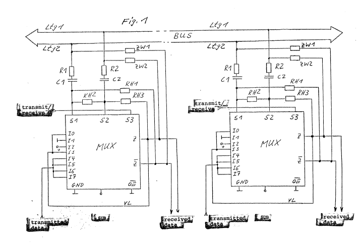
Figure 1 shows the subscriber interface bus couplers
between two subscribers "SUB" and the bus 5BUS). A greater
plurality of such subscribers can be connected to the bus,
each operating as data transmitter and/or data receiver for
the exchange of data. The data are transmitted by means of
difference signals as predominantly employed in extensive
line systems because of their freedom from induction loops.
, , .
.
.
'
~ ~ S~
A commercially available multiplexer (MUX), e.g. an AC 251 in
CMOS-F~CT technology, is employed in the bus coupler. Due to
the special interconnections according to the invention, this
bus coupler meets all operational requirements, particularly
with respect to fault tolerance.
`~ The two bus lines Ltg 1 and Ltg 2 each are coupled to a
respective one of the two address inputs S1 and S2 of the
multiplexer MUX in a galvanically (electrically) separated,
i.e., d.c. blocking, manner by way of respective isolating
~10 capacitors C1 and C2 and series resistors R1 and R2. The
data inputs are marked I0 to I7 and the data outputs are
marked Z and Z for the non-inverted and inverted output
signals respectively. By way of address input S3, switching
between transmit and receive modes of operation of the
multiplexer can be made. In the transmitting mode of opera-
tion, multiplexer MUX switches the data supplied by a
subscriber via inputs I4 to I7 onto the bus via respective
resistances ZW1 and ZW2 connected to the outputs. In the
receiving mode of operation, the multiplexer MUX receives the
data on the bus via address inputs S1 and S2. Depending on
the polarity of the signals in lines Ltgl and Ltg2 of the
bus, multiplexer MUX decodes, in a manner to be described
below, which signals are to be evaluated as received data.
-- 8
2 ~ fi~
In the transmit operational mode, a logic H (high)
signal is applied to address input S3. The multiplexer
inputs I4 to I7, which are all connected together and receive
the data to be transmitted, are then switched to the bus. It
does not matter what potentials the other address inputs Io~
I3 have ("don't care" state).
Multiplexer MUX has the following truth table:
S-3 ~ I S2 Sl
L L I0
, L L H Il
L H L I2
L H H I3
H L L I4
H L H I5
H H L I6
_
H . I7
Multiplexer input Il is connected to ground ("L" low
potential) while input I2 carries a positive voltage ("H"
high potential). Inputs I0 and I3 are each connected with
data output Z. With this type of connection, and the truth
table of multiplexer MUX above, only the push-pull states of
the bus signal at address inputs Sl and S2 are decoded as
fixed logic levels (multiplexer inputs Il and I2) in receive
"''' . ~:
2~2~3r7~$
operational mode (when address input S3 carries a logic L
signal), while ~or common-mode states (multiplexer inputs I0
and I3), the last, previous, logic levels are used as a
result of the signal feedback through connecting line VL from
data output Z of multiplexer MUX to the inputs I0 and I3
whose binary coded ranking corresponds to the common-mode
states 00 and 11. Thus, common-mode interference is always
returned to the previous level and thus suppressed. However,
the signal feedback is effective only in the receive opera-
,10 tional mode. In the transmit operational mode, it is sup-
pressed be~ause the presence of an H potential at address
input S3 permits only signals at inputs I4 to I7 to be effec-
tively switched through.
Address inputs S1 and S2 are biased by hysteresis
resistors RH1, RH2 and RH3. These hysteresis resistors ~H1,
RH2 and RH3 are arranged as follows: hysteresis resistor RH1
is connected between address input S1 and the Z data output
of multiplexer MUX; hysteresis resistor RH2 is connected
between address inputs S1 and S2; and hysteresis resistor RH3
lies between address input S2 and the Z data output. The
bias at address inputs S1 and S2 is generated by the voltage
drops across hysteresis resistors RH1, RH2 and RH3.
The d.c. voltage values lost due to the d.c. voltage
electrical blocking or isolation (capacitors C1, C2) are thus
- 10
., , ~
2~7~i
re-introduced in the form of a d.c. bias at address inputs S1
and S2. This re-introduction of the d.c. voltage values is
important to achieve fault tolerance, as will be described
further below.
A signal edge having a difference character (a positive
edge at one input and a negativ~ edge at the other input) is
thus fed back via the hysteresis resistors.
The following operation results:
With the bus system completely intact (no short circuits
or interruptions at the subscribers and in the bus couplers)
and in the transmit operational mode, the transmitted data
~rom one subscriber are switched via his multiplexer MUX from
inputs I4 to I7 to outputs Z and Z, respectively, and fed to
the bus via resistors ZW1 and ZW2 which are each connected
between a respective data output Z or Z and a respective bus
line Ltgl or Ltg2. If multiplexer MUX is short-circuited at
data outputs Z and Z, the bus is thus passively terminated by
resistors ZW1 and ZW2. These resistors ZW1 and ZW2 are
advantageously selected so that their combined resistance is
equal to the characteristic impedance of the bus~ e.g. 100
ohm. If there is a short circuit at address inputs S1 and
S2, the bus is terminated by resistors R1, R2 and ZWl, ZW2.
Thus, there exists complete fault tolerance; that is, a fault
~ uJ~
at a subscriber or his bus coupler does not lead to inter-
ference in the operation of other subscribers using the bus.
Figures 2 to 4 show the voltage curves over time for a
received data signal (the respective upper signal) and the
signal shape resulting on the bus from the transmitted signal
if interference is present (the lower signal in each case).
In the case of Figure 2, a superimposed interference exists
in the form of a 100 kHz rectangular signal. In the case of
Figure 3, a subscriber or, more precisely, his bus coupler,
~10 has encountered a short circuit, and in Figure 4, two sub-
scribers or, more precisely, their respective bus couplers,
have encountered short circuits simultaneously. As evident
in Figures 3 and 4, the signal amplitude on th~ bus decreases
with an increasing number of short-circuit occurrences, since
for n short circuits the bus is terminated by n parallel
connections of respective resistances ZW1 and ZW2. The
selection of the bias for address inputs S1 and S2 must be
adapted accordingly in order to realize greater fault
tolerance. If the bias is selected by appropriate dimension-
ing of the hysteresis resistors RHl-RH3 to be slightly below
the response threshold of the address inputs of multiplexer
MUX, a reliable decision can still be made in all illustrated
cases as to which type of data (0 or 1 states) were trans-
- 12 -
mitted. The following applies for the dimensioning of the
resistors:
Initially, an important requirement is that the resis-
tance of the hysteresis resistors RH1 to RH3 should be sig~
nificantly greater than resistors R1, R2, ZWl, ZW2. This
somewhat simplifies matters and lightens the load ~or the
drivers. A further simplification of the situation is
brought about by the fact that the MUX components are not
true difference drivers or receivers but normal FACT gate
networks. Thus, it is possible to consider the outputs and
inputs of the multiplexer to be electrically isolated. Only
the logic linkage makes the circuit a difference stage. This
then operates as follows:
A driver presently transmitting impresses a push-pull
1~ voltage at the driving impedance Zw (Zwl = ZW2) onto the bus.
For k subscribers the existing load is:
Z1 = Zw/k.
Resistors RH1 to RH3 are neglected because of their high
resistance values, as already mentioned. The equation
results because at the first moment of switching, the end of
each impedance Zw remote from the bus is connected to an
output of the receiver (Z, Z). The latter is set (FACT) to
the ideal of O ohm. Thus, the voltage jump at the inputs S1
- 13 -
2 ~
and S2, respectively, is as follows (line effects are
neglected here):
U(S1,2~ = 5 V (Zw/k).(Zw/k + Zw)
or U(S1,2) = 5 V ~ k+1)
where 5 V is the supply voltage for the respective multi-
plexers MUX.
Thus, the voltage jump is determined only by the number
of subscribers. The more subscribers, the smaller the
voltage jump becomes, so that this number also limits the
system.
The set hysteresis value must be dimensioned correspond-
ingly. Of course this voltage jump must exceed the hyster-
esis since otherwise the receivers would never be able to
switch and would thus be unable to "assist". Therefore, the
exponential drop of the capacitor ~oltages at the input from
a preceding jump must settle at no more than:
Uhsl+ = 5 V (RH2+RH3).(RHl+RH2-~RH3) - 2.5 V < U(S1)
and
Uhs2+ = 5 V (RH2+RHl).~RHl+RH2+RH3) - 2.5 V < U(S1)
above the 2.5 V threshold, depending on which input happens
to receive the "HIGH" signal. The same applies correspond-
ingly for the "LOW" signal as is easily understood on the
basis of symmetry considerations.
- 14 -
2 ~
The following then applies:
Uhsl- = 2.5 V - 5 V (RHl) (RHl+RH2+RH3)
and
Uhs2~ = 2.5 V - 5 V (RH3) . (~Hl+RH2+RH3)
below the 2.5 V threshold. (By equating Uhsl+ and Uhsl- as
well as Uhs2+ and Uhs2- it can easily be proven that this
equality and thus the symmetry of the hysteresis is actually
the case.) As long as these hysteresis, as already men-
tioned, are still traversed in push-pull, the receiver will
~10 respond.
If short circuits occur, it depends on whether these
occur at the outputs Z, Z or at address inputs Sl, S2 of
multiplexer MUX and both cases must be considered. In the
case that one of the outputs Z, Z short-circuits, nothing
changes in the edge voltage on the bus because the transmit-
ter continues to "see" the above-calculated load. The only
thing different is that the assistance after exceeding the
threshold no longer occurs which, however, is not critical
since the switching process is then already completed. If,
however, a short circuit occurs at one of the address inputs
Sl or S2, this load is connected in parallel with the respec-
tive resistors Rl,R2. However, for the sake of speed, the
resistance of these resistors R1, R2 cannot be selected to be
too large. The order of magnitude in any case mus!t be Zw.
- 15 -
. . .
. .
Thus for n short circuits the load fQr the transmitter is
calculated as follows:
Z1 = 1/(k/Zw + n/R).
In that case, because of the voltage division, and by
substituting this new value of Z1 into the previous equation
for U(S1,2), the voltage at the address input (Sl,S2) becomes
the following:
U(S1,2) = S V [1/(l+k+nZw/R)]
The previous or old value of U(S1,2), which includes
~10 only the number of subscribers, then results for n = 0.
The number of tolerable short circuits now again depends
on the value to which the voltage across the receiver input
is permitted to drop; that is, the value of the hysteresis
voltage (Uh) which, however, is the following:
15Uhsl+ = 5 V (RH2+RH3).(RHl+RH2+RH3) - 2.5 V
Now symmetry can again be presumed to exist without
limiting general applicability, that is, the pure hysteresis
voltage amount can be used with RH1 = RH3 = Rh and RH2 = Rhd:
Uh = 5 V (Rhd+Rh).(2Rh+Rhd) - 2.5 V
20And, with Uh < U(S1,2), a solution toward n brings the
following:
n < R/Zw [4Rh/Rhd - (k-1)]
for the tolerable number of short circuits. As can be seen,
R (the resistance ahead of the capacitor) is included in the
- 16 -
-, - , .
2 ~
fault tolerance. For one specific embodiment, the following
dimensions applies:
R = Zw; Rh/Rhd = 7; k = 8
so that theoretically n = 21 is permissible; that is, a
value far above the number of subscribers. The reasons for
this high fault tolerance are the following:
(a) the large dimensions of ~h/Rhd (the hysteresis was
only about 0.35 volt) which is affordable due to the binary
common-mode suppression;
(b) the fact that the here calculated worst case of an
input short circuit is much less frequent than the short
circuit of an output. But then no increased load acts on the
transmitter. More short circuits than subscribers can happen
only if one subscriber has several defects simultaneously.
That case is even rarer.
With difference signal transmission, the high signal to
noise ratio permits a very low hysteresis setting. Because
of the binary common-mode suppression, it does not matter at
all if peaks go through it.
The measures according to the present invention allow a
quasi-synchronous start-stop-bit operation. Due to the
signal feedback from the Z output to the I0/I3 inputs, one
stop bit remains in the bus "memory" during the "guard time".
- 17 -
'' ' '
.
2~7~
It will be understood that the above description of the
present invention is susceptible to various modifications,
changes, and adaptations, and the same are intended to be
comprehended within the meaning and range of equivalents of
the appended claims.
. - 18 -