Note: Descriptions are shown in the official language in which they were submitted.
-1-
STATISTICALLY BASED CONTINUOUS
AUTOCALIBRATION MEI'EiOD AND APPARATUS
Field of the Invention
The present invention relates to the calibration of sampled systems, and
more particularly relates to the automatic statistical calibration of such
systems to
compensate for parameters that may cause such systems to deviate from ideal.
Background and Summary of the Invention
- For expository convenience, the present invention is described with
reference
to one illustrative application thereof, namely a system for removing
conversion errors
in a subranging analog-to-digital conversion circuit (ADC). It will be
recognized,
however, that the invention is not so limited.
A typical subranging ADC 10 is shown in Fig. 1. It includes a track and
hold circuit 12, first and second ADCs 14, 16, a digital-to-analog converter
(DAC) 18,
a load 20, an amplifier 22, and a summer 24. In operation, an input analog
signal is
applied to the track and hold circuit 12. The output from this circuit tracks
its input
until a clock signal applied thereto causes the circuit to momentarily hold
its output
fixed. The first ADC 14 then converts this analog output signal into digital
form,
thereby providing a first approximation of the digitized value.
The digital output from ADC 14 is converted back into analog current form
by the DAC 18, causing an error, or residual voltage to be developed across
the load
20. This residual voltage is amplified by the amplifier 22 and converted into
digital
form by the second ADC 16. The accuracy of ADCZ is less critical than ADCl
since
it is only operating on the residual or "subrange" of the original signal. In
the Fig. 1
system, the errors of ADCZ are only one 64th as significant as errors in ADCl.
The summer 24 sums ADCI's first approximation of the input analog signal
and ADC2's representation of the residual (appropriately adjusted for the gain
of the
amplifier) to provide a composite digital output signal.
The advantage of the subranging approach is that the accuracy of the result
is dependent only on the accuracy of the DAC and ADC2, not on the accuracy of
ADCl. The size of the residual is still a function of ADCl accuracy but the
accuracy
of the residual is not. This shifts the primary accuracy requirements to the
DAC
instead of the ADC, taking advantage of the inherently higher accuracy of DACs
for a
given sample rate.
-2-
The principal limit on accuracy in subranging ADC' 10 is the accuracy with
which the DAC 18 converts the digital output of ADC1 14 back into analog form.
The DAC 18 typically generates its output signals by controllably gating
binarily
weighted currents into a summation node in response to the bits of the digital
input
signal. The magnitudes of these component current sources are set by resistors
internal to the DAC. High accuracies can be achieved by laser trimming each
resistor
in each DAC to achieve a desired measure of accuracy. However, such custom
processing makes the DAC expensive and thus unsuitable for many applications.
Mass
produced DACs are much less expensive but can significantly compromise the
accuracy
of a subranging ADC.
To permit use of mass produced DACs in subranging ADCs, a technique has
been developed wherein the error of each of the DAC current sources is
quantified,
and the resulting subranging ADC output signal is compensated for their
cumulative
error. Fig. 2 shows such a system. The correction circuit 26 includes a memory
in
which the error of each of the DAC's current sources is stored. By monitoring
the
digital signal applied to the DAC, the correction circuit 26 can determine the
current
sources that are active, calculate their cumulative error, and subtract this
error from
the final subranging ADC output signal.
While the foregoing technique provides high accuracy without precision
DACs, it requires a calibration cycle in which each of the DAC current sources
is
individually operated, its output current compared against ideal reference
values to
quantify its error, and the error terms stored. One difficulty with this
procedure is
that of obtaining the requisite ideal reference values. More troublesome is
the fact
that the DAC errors change with age, temperature, and a variety of other
factors,
requiring recalibration periodically if accurate results are to be achieved.
To overcome these difficulties, the present invention provides a technique
wherein the errors of the component DAC current sources are determined
automatically during the circuit's normal operation. This is achieved, in a
preferred
form of the invention, by continually introducing a random signal into the
process,
statistically examining the DAC output signal to discern error terms, and
correlating
the occurrences of these errors with the values of the random signal applied
to the
DAC so as to identify the current sources to which the error terms are due.
The
resulting output signal is compensated to remove the random signal and is
further
compensated to remove the DAC error terms discerned by this statistical
analysis.
CA 02029944 1999-08-09
-3-
The effect of any errors that may remain due to imperfect quantification of
the DAC
error terms is minimized because these errors are now random, permitting them
to be
removed by averaging techniques.
Other aspects of this invention are as follows:
In a subranging analog-to-digital converter that includes:
first and second analog-to-digital converters (ADCs) each having an input and
an
output;
a digital-to-analog converter (DAC) having an input and an output;
an analog subtraction circuit having first and second inputs and a difference
output;
an analog signal input connected to the first input of said subtraction
circuit;
said first ADC having its input connected to said analog signal input and
having its
output connected to the input of said DAC;
said DAC having its output connected to said second input of said subtraction
circuit;
said second ADC having its input connected to said difference output of said
subtraction circuit; and
means for combining the outputs of the first and second ADCs to provide a
digital
output signal;
2 0 an improvement wherein the DAC comprises:
first, second and third DACs, each having an input and an output;
first and second digital noise sources, each having an output;
first and second adders, each having two inputs and an output; and
a correction circuit having a plurality of inputs and an output;
2 5 said first adder having its first input coupled to said output of said
first noise source
and having its second input coupled to said output of said first ADC, said
first adder having
its output coupled to said input of said first DAC to provide the negated sum
of the first noise
source output and the first ADC output thereto;
CA 02029944 1999-08-09
-3a-
said second adder having its first input coupled to said output of said first
noise
source and having its second input coupled to said output of said second noise
source, said
second adder having its output coupled to said input of said second DAC to
provide the sum
of the first and second noise source outputs thereto;
said third DAC having its input coupled to said output of said second noise
source
for receiving a negated noise output therefrom;
said first, second and third DACs having their outputs coupled to said second
input
of said analog subtraction circuit;
said correction circuit having a first input coupled to said output of said
second ADC,
a second input coupled to said output of said first adder, a third input
coupled to said output
of said second adder, and a fourth input coupled to said output of said second
noise source;
said circuit including means for compensating the digital output signal for
conversion errors
in said first, second and third DACs.
In a subranging A/D methodology that includes the steps:
generating a digital approximation of an analog input signal;
converting said digital approximation into an intermediate analog signal
approximately corresponding thereto;
producing an analog subrange signal by determining a difference between the
analog
2 0 input signal and the intermediate analog signal;
generating a digital approximation of said subrange signal; and
combining said digital approximations to yield a final output signal;
an improvement wherein the D/A converting steps includes:
summing the digital approximation of the analog input signal with a first
digital
2 5 noise signal to yield a first sum;
producing a first analog signal that approximately corresponds to the negative
of said
first sum;
summing the first digital noise signal with a second digital noise signal to
yield a
second sum;
3 0 producing a second analog signal that approximately corresponds to said
second
sum;
20 29944
~,
-3b-
producing a third analog signal that corresponds to the negative of the second
digital noise signal; and
summing the first, second and third analog signals to yield the intermediate
analog signal.
In a subranging A/D methodology that includes the steps:
generating a digital approximation of an analog input signal;
l0 converting said digital approximation into an intermediate analog signal
approximately corresponding thereto;
producing an analog subrange signal by determining a difference between the
analog input signal and the intermediate analog signal;
generating a digital approximation of said subrange signal; and
combining said digital approximations to yield a final output signal;
an improvement wherein the D/A converting steps includes:
combining the digital approximation of the analog input signal with at least
one
digital noise signal to yield a digital combined signal;
converting the digital combined signal into a first intermediate analog signal
2 0 approximately corresponding thereto using a DAC;
processing said first intermediate analog signal to remove the noise component
thereof; and
for at least one bit of the DAC;
correlating the final output signal with a digital value applied by the
digital
2 5 combined signal to said bit to note any deviation from ideal DAC behavior.
In a method of compensating conversion error in a digital-to-analog converter
(DAC) used in a subranging analog-to-digital converter (ADC), said method
including
applying an input signal to the DAC and compensating an output signal produced
by
3 o the ADC using an error term associated with said DAC input signal, an
improved
method for characterizing the error term comprising:
stimulating the DAC with a random signal; and
CA 02029944 1999-08-09
-3c-
discerning the error term based on the statistical behavior of the ADC output
signal.
In a method of converting a desired input digital signal into an analog signal
corresponding thereto, said method including stimulating a digital-to-analog
converter and
compensating a resultant output signal using an error term associated with the
stimulus, an
improvement comprising:
estimating said error term while converting the desired input digital signal
into an
analog signal corresponding thereto, rather than in a dedicated calibration
cycle.
In a method of quantifying errors of signal sources in a digital-to-analog
converter
(DAC), an improvement wherein a reference against which the signal sources are
compared
is generated by:
including the DAC in an electrical system;
stimulating the DAC with a random signal; and
statistically analyzing the behavior of a signal produced by said system.
A method for compensating a sampled data process F by removing
deviations therefrom to make it more nearly ideal, said process being ideally
represented as:
F(Xn) = Yn
where Xn is an input and Yn is a scaler output corresponding thereto;
2 0 said process actually including one or more process parameters that cause
the actual
process to deviate from ideal so that the actual process is represented as:
F(Xn,Pn) ° Yn
where Xn is the input, Pn is a vector representing the parameters for the
corresponding
sample, and Yn' is the output of the actual process corresponding to (Xn,Pn);
2 5 the process being such that:
F(Xn) = F(Xn~P)
where P is a fixed vector representing ideal process parameters;
the method comprising the steps:
providing a random vector Zn;
20 29944
-3d-
performing an operation C on (X",Zn) to yield an output Xn';
performing the operation F on (X"',P") to yield an output W"';
performing an operation H on (Xn,Z") to yield a vector output Z"'; and
performing an operation D on (W"',Z"') to yield an output Wn;
calculating the parameter vector P"+1 for the next sample using the formula:
Pn+1 = Pn - ~wri Zn~~~
where K is a smoothing constant;
wherein:
operations C, H and D are chosen such that:
wn = Yn = F~xn~P) - D~Wxn~Zn)~P)~H~xn~Zn))
and:
the sign of each element of the expected value of [W"Z"'] is the same as the
sign of the corresponding element of the expected value of [P"P].
The foregoing and additional features and advantages of the present invention
will be more readily apparent from the following detailed description thereof,
which
proceeds with reference to the accompanying drawings.
Brief Description of the Drawings
Fig. 1 is a schematic block diagram of a prior art subranging analog to
digital
converter circuit.
Fig. 2 is a schematic block diagram of a prior art subranging ADC that
includes
2 5 compensation to remove known DAC errors.
Fig. 3 is a schematic block diagram of a subranging ADC that includes
statistical autocalibration according to one embodiment of the present
invention.
Fig. 4 is a schematic block diagram of a correction circuit used in the
subranging ADC of Fig. 3.
3 o Fig. 5 illustrates an ideal process.
Fig. 6 illustrates an actual process that includes a non-ideal process
parameter P.
ZO 29944
- 3e -
Fig. 7 is a schematic block diagram of a generalized embodiment of the present
invention.
Fig. 8 is a schematic block diagram of Fig. 7 annotated to detail the
correspondence of its generalized functional blocks to their particular
functions in the
subranging ADC of Fig. 3.
Fig. 9 illustrates an intermediate specialization of the generalized
embodiment
of Fig. 7 to a particular gain controlled amplifier embodiment.
1 o Fig. 10 illustrates another intermediate specialization of the generalized
embodiment of Fig. 7 to a particular gain controlled amplifier embodiment.
Fig. 11 is a schematic block diagram of an application of the generalized
embodiment of Fig. 7 to a particular gain controlled amplifier application.
Detailed Description
The subranging ADC with which the present invention is illustrated minimizes
errors associated with non-ideal digital-to-analog conversion by two
techniques. The
first is to automatically quantify the error of each of the DAC current
sources so the
final digital output signal can be compensated for their cumulative error. The
second
-4-
is to randomize any remaining errors that may be due to imperfect
quantification (and
thus compensation) of the DAC current source errors.
RANDOMIZATION
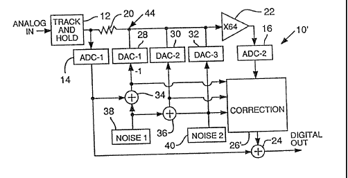
Fig. 3 shows a subranging ADC 10' employing the techniques of the present
invention. Taking the randomization technique first, the single DAC of Figs. 1
and 2
is replaced by three DACs 28, 30, 32, two adders 34, 36, and two noise sources
38, 40.
Since all three DAC current outputs are wired in parallel, the composite
output is
DACI + DAC2 + DAC3. (This summation is performed at a current node 44.)
Assuming perfect DACs and tracing the DAC inputs back through the adders, the
composite output can be seen to be -(ADCl + NOISE1) + (NOISE1 + N01SE2) -
(NOISE2), or -ADCI. This is the same effective DAC output as in the subranging
ADC of Fig. 1 if the three DACs are perfectly accurate. The difference arises
when
the DAC errors are considered.
In the subranging ADC of Fig. 1, DACl is driven directly by the output of
ADCI, which in turn is directly determined by the sampled input voltage. In
that
case, any errors produced by the DAC are repeatably generated for any given
input
voltage. Consequently, the inaccuracies of the overall A/D converter system
are
repeatable and signal dependent. This means that even if multiple measurements
are
made of a certain signal, the errors cannot be averaged away since they are
signal
dependent and are repeated in all measurements.
In the randomized converter illustrated in Fig. 3, each DAC current source is
driven by a bit stream which is determined by pure noise, or by noise combined
with
signal bits. If the noise signals are appropriately selexted, only the most
significant bit
of DACI has any correlation with the input signal. This means that errors due
to any
of the other bits are injected in a manner completely independent of the input
signal.
The result is a noise-like error which can be averaged away using multiple A/D
measurements. This characteristic is very beneficial in many applications.
Even
though this benefit alone is very important, a possibly more significant
outcome is that
this scheme provides a straight forward technique of determining the DAC
current
source errors for calibration.
AUTOCALIBRATION
The autocalibration technique employed in the present invention relies on
two statistical properties of the system's signals. The first is that the
digital input bits
applied to the three DACs are random (with the exception of the MSB of DAC1,
as
~02994~
-S_
mentioned above). Consequently, it is equally probable during any given
conversion
cycle that any given input bit may be a "1" or a "0." The second statistical
property is
that the final output signal from the A/D converter is uncorreiated to the
values of
the DAC input bits, since the input bits are randomized. (The interconnection
of the
three DACs in the manner illustrated cancels out the random noise component
from
the final output signal, as noted above.) Due to these two conditions, it is
known that
the long term average of the system output signal when a given input bit of a
DAC is
a "1" should be exactly the same as the long term average of the output signal
when
the given input bit is a "0."
If the long term average of the output signal when the given input bit is a
"1" is not exactly equal to the long term average of the output signal when
the input
bit is a "0," then one of the two statistical assumptions is incorrect. If the
randomization of the digital input bits is truly a random process, then the
assumption
that "1"s and "0"s are equally likely is known to be correct. Consequently,
any variance
between the two long term averages must be due to a violation of the other
assumption. Namely, there must be some correlation between the value of the
given
DAC input bit and the system output signal.
Such a correlation may be due to a variety of factors. However, the
dominant factor is the error by which the magnitude of the DAC current source
differs
from its ideal value. Assuming for a moment that all of the DAC current
sources
except one are ideal, and that this one current source is slightly larger than
it should
be, it may be recognized that the system's long term average output signal
when that
current source is energized will be slightly larger than the long term average
output
signal when that current source is idle. This is due to the slight additional
current
associated with this current source (but none of the others) that is added to
the final
output signal each time this current source is energized but is not added when
it is
idle. By examining the behavior of the output signal over the long term and
correlating its behavior with the value of a given DAC input bit, the error of
the
associated DAC current source can be discerned.
This correlation is effected by adding a greatly diminished version (i.e. by a
factor of thousands or millions) of the corrected output signal to the error
value
stored in the correction circuit 26' if the corresponding DAC input bit is a
"1", and
subtracting the same value if the corresponding DAC input bit is a "0." If the
long
term average of the output signal when the bit is a "1" is the same as the
long term
average when the bit is a "0," these additions and subtractions will cancel,
leaving an
error term of substantially zero. However, if one of the two long term
averages is
202~~4
'''_' _ 6 -
larger than the other, this difference will be manifested as a non-zero
accumulation of
these added and subtracted values, thereby providing a correction value that
can be
subtracted from the output signal whenever that DAC input bit is energiTxd.
An analogy may be made to a statistical examination of the process of
wagering on a coin toss. If a bettor wins $1.01 each time he calls the coin
toss
correctly but loses only $1.00 when he calls it incorrectly, he will not break
even over
the long term. Rather, he will come out ahead. A statistician who knows the
bettor's
winnings (or losses) over the long term can discern the difference between the
two
figures. If, after a million coin flips, the bettor has accumulated net
winnings of
$10,000, and the statistician knows the bettor loses $1.00 each time he calls
the coin
toss incorrectly, the statistician can compute that the bettor must win $1.01
each time
he calls the toss correctly. The present invention relies on basically the
same
principle.
It will be recognized that, unlike the prior art, in which the error term of
i5 each current source is determined by comparison with a known current
source, the
"known" in the present invention is the expected statistical behavior of the
output
sienal over the long term as a function of each DAC input si n~al. By using
this
"known" as a basis for comparison, the error of each of the DAC current
sources can
be determined and can be subtracted out using prior art techniques.
The resulting A/D converter thus has several advantages. First is that the
DAC errors are determined automatically during the system's normal operations
and
the resulting output signal is compensated to remove their effect. The second
is that
any remaining errors are randomized, permitting their substantial removal by
time
averaging techniques.
The following discussion summarizes the necessary and sufficient conditions
for the present methodology to be effective, particularly as they relate to
the noise
source characteristics, and reviews the details of an illustrative
implementation.
NOISE SOURCE DETAILS
The proper operation of the autocalibration technique depends on the
statistical characteristics of the noise signals. , If ADCI has N bits of
resolution, then
NOISE1 and NOISE2 should have N+1 and N bits of resolution respectively. In
the
illustrated embodiment, all three of these digital signals are encoded as
positive binary
integers. If the converter is to be used for both positive and negative input
signals,
the conversion range of ADCI must be offset such that a zero volt input
produces a
half scale output. This offset can then be accounted for in the interpretation
of the
2a299~:
_,_
final digital output. Since such an offset has no effect on the operation of
the
technique being described, it will be ignored in this discussion, and the
converter will
be described as handling positive inputs only.
The N bits of NOISE2 are generated using N independent one-bit random
binary sequence generators which are interpreted collectively as an N-bit
binary coded
random integer. Since all the bits are independent of each other, all states
are equally
likely and NOISE2 is uniformly distributed in the range from 0 to 2N-1.
The N+1 bits of NOISE1 are similarly generated using N+1 independent
one-bit random binary sequence generators. N of these are interpreted as an N-
bit
binary coded random integer. The remaining random bit (0 or 1) is then added
to
this random integer. The resulting range of NOISE1 is then 0 to 2N, requiring
N+1
bits for encoding. For ease of implementation, the required addition can be
combined
with adders shown in the block diagram rather than by using a separate adder
inside
the NOISE1 source. This is done by connecting the extra random bit to the
carry-in
of each of the two adders.
Considering the range of inputs into the adders, the range of outputs is 0 to
2~N+y-1 driving DAC1, 0 to 2~N+y-1 driving DAC2 and 2N-1 for DAC3. This
implies
that the number of bits of resolution for DACl, DACZ and DAC3 are N+1, N+1 and
N, respectively. Because of the way the NOISE signals are generated and
combined
with the adders, the statistical relationships between the individual bits
streams can be
determined.
CORRECTION DETAILS
The errors associated with each of the DAC current sources by the
calibration technique are expressed in terms of their deviation from some
reference.
The choice of reference is not important as long as all the current source
errors are
consistently computed relative to that reference. The chosen reference becomes
the
"absolute" standard against which the sampled signal is measured. For this
technique,
the reference is chosen to be the current source associated with the most
significant
bit of DACl. This current reference is the absolute standard against which the
signal
current through the resistor 20 is measured. Since_ this current source is
"perfect" by
definition, it has no error and does not have to be calibrated. All the other
N+ 1 bits
used in the three DACs must be calibrated relative to the most significant bit
of
DACl. The hardware 41 used in the correction circuit 26' to apply the
calibration is
shown in Fig. 4.
20~~94L
_g_
Each of the 3N+ 1 current sources to be calibrated has associated with it in
correction circuit 26' an accumulator register 42 which holds the error of
that
particular current source. Since the desired correction accuracy is better
than the
original DAC resolution, the resolution of the accumulator must be finer than
the
resolution of the DAC. For the purpose of this discussion, each accumulator 42
may
be considered to store a fixed point two's complement binary number with M
bits to
the right of the point. The bit immediately to the left of the point is
equivalent in
significance to the LSB of ADCl, NOISE1 and NOISE2.
For each A/D conversion cycle, the first step in the correction technique is
to compute the correction needed for that sample. This is done by adders 43
that
sum up the values in all the accumulator registers associated with the current
sources
which are on for that sample, i.e. all the DAC bits driven with a "1." This
correction
value is then subtracted by a circuit 45 from the output of ADC2 to give a
corrected
residual output. This corrected residual must be computed to the full
resolution of M
bits to the right of the point.
The second step of the calibration technique is to update the accumulator
registers with new estimates of the current source errors. This is done by
dividing the
corrected residual by a smoothing factor of 2k to achieve a feedback signal
that tweaks
the error constants stored in the accumulators. The choice of a power of two
makes
the division a simple right shift of the binary representation of the
corrected residual.
After the right shift, the feedback is rounded to M bits to the right of the
point.
Each of the 3N+1 accumulator registers is updated by adding or subtracting the
feedback from the previous contents of the accumulator register. The choice of
adding
or subtracting depends on whether the DAC bit driving the current source
associated
with the register was a "1" or a "0" for the current sample. If the bit was a
"1," an add
is performed. If the bit was a "0," a subtract is performed. The result yields
the
correct value of the current source errors in the accumulator registers.
In selecting the smoothing factor 2k, there is a tradeoff between accuracy and
the speed with which the technique can track changes to the DACs caused by
aging,
temperature, ete. Choosing very large smoothing factors reduces the variance
of the
current source error estimates held in the accumulator registers, giving more
precise
corrections. However, the time constant for tracking changes in a DAC is
proportional to the sample period multiplied by the smoothing factor.
Therefore, if
the smoothing factor is set too large, the accumulator register may not
contain a very
accurate error estimate for a changing DAC error. Practical values for the
smoothing
factor range from 21° to 225.
242~4~t~
-9-
CONCLUSION ON SUBRANGING A/D CONVERSION
'The illustrated correction technique has significant advantages over
currently
used techniques in that an error model is generated and kept current without
having
to pause for a calibration cycle. The error model tracks relatively fast-
moving changes
in the DACs, allowing for greater precision. The DAC bits, excluding the most
significant bit of DAC1, are driven with noise-like signals which are signal
independent, eliminating potential self heating errors which are signal
dependent.
Most remaining errors which are not removed are randomized across the entire
frequenry spectrum, allowing for further accuracy improvement using averaging.
GENERALIZED CASE
It will be recognized that the principles employed in the above subranging
A/D converter example can be advantageously employed in a variety of other
applications. Nearly any sampled process that deviates from ideal due to
correctable
process parameters can be corrected in this manner.
An ideal process to which the methodology of the present invention may be
applied may be represented as:
F(X,i) = Yn
where Xn is an input signal and Yn is a corresponding sealer output signal.
This ideal
process is represented by Fig. 5.
The process actually includes one or more adjustable process parameters Pn
that cause the actual process to deviate from ideal. Consequently, the actual
process
is represented as:
F(~~pn) = Yn.
where 3C" is the input, Pn is a vector representing the adjustable parameters
for the
corresponding sample, and Yn' is the output of the actual process
corresponding to
(3in,P"). The process is such that:
F(Xn) = F(Xn~P)
where P is a fixed vector representing ideal process parameters. This actual
process is
represented by Fig. 6.
The application of a generalized form of the invention to correct this non-
ideal process is illustrated in Fig. 7 and follows the following basic steps.
First, a
random vector Zn is provided. Next, a preprocessing operation C is performed
on the
input signal and random vector (X,~,Zn) to yield an randomized version Xn' of
the
input signal. This randomized signal is then combined with the adjustable
parameter
- IO-
Pn and processed by the actual process F to yield an output Wn'. (That is, Wn'
_
F(Xn'.Pn).)
A second operation H is also performed on the original input signal Xn and
the random signal Zn to yield a vector output signal Zn'. (That is, H(Xn.Zn) =
Zn'.)
Finally, an operation D is performed on the signals (W"',Zn') to yield a
corrected output Wn.
The operations C, H and D are chosen such that:
Wn = ~'n = F(Xn~P) = D(F(C(Xn~Zre)~P)~H(Xn~Zn))
and the sign of each element of the expected value of (WnZn'j is the same as
the sign
of the corresponding element of the expected value of [P,; Pj.
The foregoing generalization will be made more clear by its application to
the particular subranging A/D converter 10' detailed earlier. This discussion
proceeds
with reference to Fig. 8, which is the generalized block diagram of Fig. 7
annotated to
detail the correspondence of the generalized functional blocks with their
particular
functions in the specific A/D converter example.
It may first be recognized that variable Xn here is a vector comprised of two
components: the analog signal to be converted into digital form and a digital
approximation of that analog signal. These components are labelled Vn and Aln,
respectively in Fig. 8. Pn is a set of adjustable parameters which models the
conversion errors associated with the analog-to-digital conversion process
(i.e. the
DAC current source errors stored in the accumulators 42); and Zn is a two-
component
vector of digital noise integers Zln and Z2n. The generalized preprocessing
function
C is the combination of the input signal Xn = (Vn, Aln) with noise signals Zn
=
(Zln. Z2n), i.e. C(Xn,Zn) = Xn + Zn _ (Vn, Dln, D2n, D3n), where Dln = Aln +
Xln, D2n = Xln + X2n, and D3n = X2n.
The generalized function D is simply an identity function, so that Wn' = W,1.
The generalized function H yields a vector output of -1 or 1 values
corresponding, respectively, to the (0,1) values of the individual bits of the
binary
representation of D1, D2 and D3, exclusive of the most significant bit of D1.
Finally, the generalized function F is the sum of the analog signal Vn, the
output of three ideal D/A converters driven by -Dln, D2n, and -D3n, and an
error
component for each D/A converter bit modeled by the dot product Bn ~ Pn.
By using these substitutions, it can be shown that the resulting Wn is an
accurate digital representation of the difference between the analog component
of the
input V" and the digital estimate component Aln. Thus, by adding Aln and Wn,
an
accurate final digital representation of Vn is achieved.
~o~oo~~
-11-
As noted, the present invention has numerous applications beyond the
illustrated A/D converter 10'. Fig. 11 shows a simple example - that of a gain
controlled amplifier 50. In this case, there is only one adjustable parameter
P",
namely the amplifier gain. The ideal amplifier function F is F(X",P") = X"P" =
W".
In this case, the input signal is again combined with a noise signal Z", and
this signal
is passed through the non-ideal amplifier. The resulting output signal W"' is
processed by subtracting out the noise signal that has been correspondingly
amplified.
The remaining signal is then examined for correlation with the random input
data by
the same technique used above, namely by adding or subtracting (depending on
the
random signal) a weighted version of the output signal from an accumulator
register
that determines the amplifier gain.
Figs. 9 - 10 show the series of substitutions by which the generalized diagram
of Fig. 7 is specialized into the gain controlled amplifier application of
Fig. 11. Fig. 9,
for example, shows that the function H here is simply an identity function for
the
input random signal. That is, H(X", Z") = Z"' = Z". Fig. 10 shows that the
function C here simply combines the input signal X" with the noise signal Z".
Having described and illustrated the principles of my invention with
reference to an illustrative embodiment thereof, it will be apparent that the
invention
can be modified in arrangement and detail without departing from such
principles.
Accordingly, I claim as my invention all such modifications as may come within
the
scope and spirit of the following claims and equivalents thereto.
2~2
- 12-
nrrEN~rx
The following discussion contains a mathematical description of the
~tat.istically
based correction me~t.hodology used in the illustrated subranging A/D
converter. This
description est.ablishe~ that the claimed methodology effectively removes the
effects of
errors in the digital-t.o-analog converter (DAC) current sources. The
description also
illustrates that any errors which remain after the methodology is applied can
be
represented as white noise. The discussion proceeds with reference to Fig. 12.
BLOCK DEFINING FOUATIOI~'S:
The following equations describe the functional blocks of Fig. 12 in terms of
their input-output relations.
T FI: Track and iiold
As noted, the track and hold block 12 takes a continuously changing voltage as
an input. and gencrat.es a sequence of sampled voltages on the output. Both
the input
and output voltages can take on values with arbitrarily fine resolution and
are therefore
represented as real numbers. The range of voltages on the input and output are
assumed to be limited to the range of tRIo/2, where Io is the value of the
:1ISB current
source in DACI, and R is an arbitrarily selected voltage to current scale
Cactor t.o
achieve the desired input range. Errors in the track and hold circuitry are
not affected
by the claimed methodology and are therefore not addressed in this discussion.
Expressed mathematically, the track and hold circuit 12 has the following
properties:
v(t)= A continuous real function of t, representing the signal input voltage
vs t.ime.
v"=v(t")
where: t."=.1 sequence of times at which the input is sampled;
=An integer indexing a particular sample in the sequence; and
-R~°<v"<B'~-to
nD 1: Analog-to-Digital Converter 1
2~a~
- 13-
The first AOC 14 converts tl~e sampled voltage from the track-anti-hold
circuit
12 into a binary integer. The integer is constrained to be encoded with N
hits, thus
making this representation a rather coarse approximation of the sampic<I input
voltage.
The errors associated with this coarse representation of the voltage are
carried through
the analysis as Eln. This allows veriCcation that these errors are ultimately
eliminated
through the traditional use of a two-pass (subranging) converter approach. It
also
allows verification that these errors will not adversely effect the operation
of the DAC
error correction methodology which is the focus of this analysis.
__ vn 1 ~N _
Aln ~ R Io+?)'. Eln
where: AInE Integers
0<Aln< 2N-I
N=the number of bits in ADC1
Eln=the error associated with the ADC1 conversion, and
IEln~~l.
N I F: Noise sequence generator
The purpose of the noise generator 38, 40 is to produce 21~+i uncorrelat.ed
binary noise sequences which are used to generate random integers which can be
combined with ADCI outputs to drive the DACs. At times in the following
analysis it
will be easier to consider the noise as individual random bit sequences
denoted as x;n.
At other times it wilt be easier to consider them as binary representations of
integers
D3n and D4n. V'hcn using the individual bit notation, many of the Boolean
operations
which would normally occur in describing logic operations can be more
conveniently
represented in algebraic form if the states of x;n are taken as t 1 rather
than t he
traditional 0,1 states. This eases the calculation of correlation between
bits.
xln
X~n
Xn=
x2N-f-1
~~2~~~
-1~ -
where: xinE{-1,1} is a zero mean random sequence with the statistical
proPcrt.ies
indicated in the following formula:
SnCxinbnJ-~
where: bn is any sequence which is not a function of x;n, including functions
of xi",
where m ~ n.
Note that the impticat.ions of the constraint on the expected values above are
considerable. First, if bn=1, then this constraint requires that each bit
sequence has a
50% probability in each of its two states. Second, if bn=X;~n+.n where ,n~0,
the
implication is that each sequence is "white," in that it has a uniform
spectral density.
Third, the formula requires that each sequence be totally independent of all
other
sequences and of arbitrary combinations of all other sequences. Finally, the
sequences
must be independent. oC the sampled voltage sequence. This constraint becomes
very
powerful when computing expected values of sequences which are functions of
:Cn since
any term which can be factored into the form given above will have zero
contribution to
the expected value and can therefore be ignored. Whenever this technique is
applied
subsequently in this discussion, it will be referred to as the "orthogonality
criteria."
The technique used to generate the bit sequences meeting the orthogonality
criteria will
not be described here since a variety of approaches may be used. Fortunately,
a strict
adherence to the criteria is not absolutely necessary for the claimed
methodology to
work correctly. When considering techniques for generating the noise, the
following
analysis may be consulted to see where the criteria is applied and therefore
which
orthogonality conditions are really necessary.
At times it will be more convenient to treat the noise outputs as binary
representations of integers rather than merely a sequence-of uncorrelated
bits. For those
cases, the integer sequences D4n and D3n can be defined as follows:
D XN.f.hn+1~-.~Xi 2 1 ~N_i
4n=
s=1
~a~~
- L5 -
where: D4"E Integers, 0 < D_~"< ?N
=~xN-f-1~-i,n+1 ~N_i
Dsn 2
i-1
where: D3nE Integers, 0 < D3n< 2N-1
Adders:
The adders 34, 3G described in this appendix are those which combine the
ADC1 output with the noise sequences described above. Again it will sometimes
be
convenient to think of the outputs as integers, denoted D!n and D.,n. At other
times all
three DAC drive signals will be represented as a sequence of binary vectors
Bn. In the
latter case, the binary states will again be labeled using the fl convention.
Note that
tile definition of Din implies a bit inversion after the addition of D4n-f-
D3n.
Dln= Aln'~ D4n
- ~N~-1
D2n- WD4n'f'D3n~-I
bin
62n
Bn=
63N~-l,n
where: b;nE{-1.1} , and satisfy the following conditions:
=bin ~" 1 ~N-i
D!n
i-0
=~bN+1-I-i,n+I ,~td_i
DZn ~)
i._0
-~62N-t-1-f-i,n+I ,~N_i
D3n
i=!
- 1 fi -
DAC1. DAC2, DAC3: Digital-to-analog converters and analog summation
The digital-t.o-analog converters 28, 30,.32 are assumed to be constructed as
a
set of independent binary weighted current sources with the outputs summed
together in
the analog adder (i.e. current node). The analog adder combines the DAC
current
outputs with the sampled input voltage to produce a residual voltage labeled
v~". The
main thrust of this aspect of the calibration methodology is to eliminate the
effects of
inaccuracies in the binary weighting of the current sources in the DACs. A key
assumption is that each binary bit entering the three DACs controls an
individual
current source which has a value c; independent of n and independent of the
state of all
other DAC bits. Although the c; values nominally are binary weighted within
each
DAC, this is not necessary. The methodology will remove the errors associated
with
deviations from this ideal binary weighting. The following formula gives the
composite
effect of all three DACs combined with the analog adder. No additional error
mechanisms other than the DAC current errors are modeled in this analysis.
Note that
the C vector does not include an entry for the current source driven by bo" -
the most
significant bit of DACI. This is because this current source is defined t.o be
Io and there
is no need to define a co to allow for errors in this bit relative to itself.
w~,-wn-~7~(bon'f' 1 ) -R IoI°(B~ +IT)C+5 2I°- 2No
where: I is a unit column vector, and
ct
c2
C=
~3N~-1
where: c; is a real number; and
Iocs represents the current associated with the ~th DAC bit which is driven by
b;".
- 17-
ADC2: Analog-to-nigital Converter 2
The purpose of the second ADC 16 is t.o convert the residual voltage from t.hc
analog adder into digital form. Because of the finite number of bits in ADC2,
the
output becomes a quantized a.ppro~cimation of the real value of the. residual.
The error
in this quantization will be denoted as EZ" and is carried through the
remainder of the
analysis in order to show that it has no adverse effect on the correction
algorithm.
Normally, the residual voltage range is considerably smaller than the original
input
voltage. This allows ADC2 to operate over a smaller voltage range than ~1DC1,
making
IE'nI«IEtnI' The particular encoding scheme used for ADC2 is not important,
although for this analysis it is assumed that the output is bipolar and
centered around
0.
A3n=? ~lo ~~'E3n
w here: AZ" is a rational numlxr encoded in A4 bits from ADC2; and
E="= the error in quantizing the real number v"~ to a rational representation.
Correction Circuitry:
The purpose of the correction circuitry 26 is to correct each sample of the
quantized residual by adding an appropriate correction for each bit which
drove the
DAC current. sources when that. sample was taken. By doing this, the DAC
current
errors can be removed. Even though the DAC model described above implies that.
a
DAC current error only occurs with the drive bit equal to 1, the correction is
applied for
both the 1 and -1 states. Although this seems counter-intuitive, it actually
yields better
statistical properties for the errors inherent in the correction algorithm.
The corrections
applied to the residual are based on an error table which stores a
representation for the
error of each DAC bit relative to the A4SB of DAC1. There is no correction
applied for
the 114SB of DAC1 since it is defined as the reference Io. The generation and
updating of
the error table will Ix described in the following section.
~0~~~:
- 18-
Gn=A=n-finTlin
where: Ii" is a rational vector described below; and
Gn is a rational staler.
Correlation:
The purpose of the correction hardware 41 is t.o updat.e the correction
vector,
IIn, based on the corrected residual and on the DAC drive bits for the current
sample.
This block maintains a running accumulation of the corrected resi<lual times
each DAC
drive bit.. If there is a correlation between these two sequences, the stored
correction
value will integrate to a new value until the correlation disappears. When the
corrected
residual no longer correlates to any of the DAC bits, the correction vector
contains the
appropriate values to offset the DAC current errors. The fact that this occurs
and that
the vector is independent of the input signal will be shown later.
lln+1=Hnd-Bn hn
where: Ii" is a vector of rational numbers; and
Iv is a large integer.
Outnut Addcr:
The output adder 24 combines the coarse quantization results from ADC1 with
the corrected residual to generate the composite digitized output from the
converter.
Yn=Aln'f'Gn
DERIVATION OF RESULTS
The following discussion contains the derivation of the output signal in terms
of
the above definitions. Only the main flow of the derivation is given in this
section,
while details for specific steps are given in the following section laheled
Supporting
Derivations.
- 19-
The first part. of this analysis calculates the deterministic portion of the
output.
The second part. then examines the nature of the random noise which is
inherent in the
svst.em.
Computation of G~. I1~, and Yes:
Using the defining equations from the previous section, the output 1'n can be
computed in terms oC vn. Since Ale is already defined in terms of v" , the
challenging
part of this derivation is to determine the corrected residual, Gn, in teens
of v". The
defining equation for G" can be expanded by substituting in the definitions
for A~" and
then v;,. Regrouping and factoring yields the following result.
Gn=2N~~I -b~.+I -~Bn 2 IT)(C+21 NHn),+~~...
0
-I ~-Eye+ITIi"
The factor (C-f-21-NIIn) becomes, in effect, the corrected current source
weights for the
DAC bits relative to the rISB of DAC1. These corrected bit weights will be
designated
as W.,. Ideally Wn would not change versus n and would be binary weighted
values
within each DAC. In order to sec if the correction algorithm approaches this
condition,
the characteristics of ~V" must be derived. This may be done by taking the
de(5ning
equation for IIn, multiplying both sides by 21-N, adding C to both sides, and
substituting in ~Vn and Gn. The resulting equations for the corrected
residual, G", and
the effective bit weights, 'Vn, are:
Gn=2"L RI I bo ~+I-B~ ~+ITW"'t'~~...
0
-I+E~"+2N-1IT(~Vn-C)
where: ~Vn=C~-21-Nlin
wn+1-(I-BnRnT~ 'Vn ...
-20-
+ fl\r~ II,In bOn-lT~'r'i-4-?1 N~-21 NCon
0
The recursive equation for ~V'" can be solved by breaking ~~'n down into a non-
varying
component, W, and a zero mean varying component, W;,.
~Vn=~V~-V~'n
where: W=6n~«'n)= the expected value of Wn.
Taking the expected value of both sides of the recursive equation for ~'Vn+t
and
applying the subst.it.ut.ion indicated above yields the following:
W=gr~~~I-BnRnTI ('y-~Wa)+B' ~ RIn bon-ITC+4-21-N-f-?1 NE2n)
\ / 0
The ort.hogonality criteria, described in the preceding discussion defining
the
noise, can now be applied. By examining each element of Bn , it is found that
each
term of each entry can be factored according to the orthogonality criteria and
therefore
has a zero expected value. (See the derivation for Bn in the following section
on
Supporting Derivations.) The term B"BnT~Vn also has a zero mean since ~V;, has
a
zero mean and it contains no terms with x;n values in common with Bn. This is
because ~Vn is a function only of previous Bn vect.ors and not current vectors
(gee the
recursion formula above for Wn).
W=(I-~) W- ~°
where: F=6n(B"BnT~
Fo=6n~Bnbon~
W=-F-tFo
The derivations of F and Fo are given in the section on supporting
derivations.
By performing the matrix inversion and multiplication indicated above, ~V
becomes:
_~l-
A
I
~V =
A
A
I/2
I/4
where: A =
I/~N
G" can now be rewritten in terms of VV and 'V;, as follows:
G"=2N v" _bon+1-B"T-l-ITW+5
C RIo 2 2 2~"'
-I-1-E,,"+2N-1IT(~V-C~-2N'1B"T~,'lri
By substituting in the bit based definitions for D1", Dz", and D3" it can lie
seen that:
Gn=2NC Rio_2-N(D~"+ p,,"-f-Dgn~~'2~~..
-I+E.,"+2N-1IT(W-C)-2N-1B"TWn
By subsl.ituting the integer based definitions for D1", DZ", and D3" it can be
seen that:
Gn=2NL RI 'f-~~-AI"~.'E~"...
0
+ 2nf 1IT(~V-C)_~N-iB"T~yn
The final output then becomes:
Y"=2~ IZIo+~,'~'E~"-f-E3-2N-iB"TVy~
where: E3=2N'lIT(~V-C)
The first term in the above equation for Y" is the ideal desired output. The
2~~~~~
:,
second term is tl~e error caused by the quant.izat.ion and inaccuracies of
ADC3. The
third term, E3, is a static inaccuracy due to the deviation of actual current.
source
values, C, from the ideal current source values, ~'~'. The last term
represents a zero-
mean noise error which is injected by the correction methodology. The
magnitude and
spectral charact.erist.ics of this noise are computed in the following
discussion.
If E3 is traced back to its origin in the above derivation, it is seen to come
from
the use of a bipolar versus unipolar application of the correction factors. E3
could be
eliminated by reverting to the more intuitive technique of adding a.
correction only when
the corresponding DAC bit. is turned on. Unfortunately, this leads to an
additional
component in the recursion equation for ~~';,, and this additional component
gives rise
to a non-white noise characteristic for the final term in the above equation
foe 1'n.
Since the track-and-hold will have imperfect DC performance anyway, it was
determined that the small DC error, E3, was preferable to having a non-white
noise
spectrum. hence, the bipolar correction technique was adopted.
Comontation of Noise. IinTWn
The spectral characteristics of the random noise portion oC the output. can be
derived by forming the autocorrelation function of the noise, and then
transforming to
the frequency domain. Let the autocorrelation function, Pm, be defined as:
Prrr=b°n~.~N 1'V~T BnBn-m ~N 1"~~-m,
By using the definition of Itn+tr adding 2N-1C to both sides, and substituting
in the
decomposed representation for Wn, the following result is derived:
~N lwn+1 = 2IJ 1'yn-f-B' Gn
If Gn is written as a sum of a deterministic portion plus a random portion,
the
expression hccomcs:
Gn=Gir-~N lBuT«'n
-23-
where: Ga=?NL ~Io'f'~~-Atn+Esn- Es
C=;, is a staler sequence which represents the corrected residual without. the
random
algorithmic noise. In fact, by applying the definition of Atn Gn can Ix
rewrif.t.en as:
Go=Etn+E~n+E3
~V~ I B"B"T V~'n~-1-21-N B"G~
n+t -~ I~ ) h n
Let the matrix inside the parentheses be represented by its expected value
plus a zero-
mean varying component, p"/IC. The expected value has already been defined in
terms
of F such that
~Vrn+t=( 1-~) «~n~+ ~n~V~-i-21-N ~ G"
To simplify the analysis, assume that the middle term above can he ignored.
The justification for this is that since an is zero mean, and since ,~nand
~'V;, do not
correlate with each other by virtue of being functions of non-overlapping sets
of random
binary sequences, the mean value of the middle term is zero. Because of this,
there is no
cumulative effect due to this term when the recursion relation for 'V;, is
expanded. As
a contributor of random noise, the middle term is small compared with the
t.ltird term.
This is because the entire calibration methodology is dependent on applying
enough
averaging (i.e. making IC large enough) such that the fluctuations in the
correction
factors, ZN-1 ~Y;,, arc very small compared with the corrected residual, G;,.
Using these
assumption yields:
n
~V~"+1=( 1-h) ~~n~~''Z1 N
This recursion relation can now be expanded in terms of an infinite series as
follows:
~ 1-N ~ l
~V~n=..h ~~1-h~' B"-'-tGl"-'-1
i= \o
The term in parentheses is a real symmetric matrix. Therefore, there exists a
unitary
202~~~4:
-24-
transformation that will diagonalize that matrix. More specifically:
I-~ =~TA~
where: ~T=~'I; and
A is a diagonal matrix.
Substituting into the definition of P,n yields:
Pm=b°" ~~(~C-Tin-iBn-i-1 ~TA'~~BnBn-m ~~~TA~~ Bn-",-j-lC'/n-m-j)
~=0 ~=0
At this point. the orthogonality criteria can again be applied to eliminate
many of the
terms in the expansion of the product of summa.t.ions. Note that every term in
the
expansion has four factors involving by, where q takes on the values n-i-1, n,
n-m,
and n-m-j-1. Since each by can be factored into the form described by the
orthogonalit.y criteria, it follows that the product. of four of these terms
can also be
factored into that form unless the four subscripts appear in two equal pairs.
For
example: when n=n-m and n-i-1=n-m-j-1, the xQ values are paired up in the
product. and the orthogonality criteria no longer holds. Therefore, terms of
this type
must be saved in the expected value computation. Inspection of the possihle
combinations shows that only the case used in the example above yields terms
which do
not meet the orthogonality criteria. In other words, the only terms which must
be
considered are those where .n=0 and i=~. «'e can therefore rewrite Pn, as:
~ , if m~0
Pm=
~Z~bnCGin-iB,T~_i_1 $TA'~BnB~ ~TA'~ Bn-i-lGin_;~ , if m-0
i=0
Since n~n-i-1, for any allowable value of i, the expected value of the product
B"Bn
can be computed independently of the summation over i. For this reason we can
write:
l~~~nCGin_;B,T~-i-1 ~TA~$F~TA'~ Bn-i-iGin-iJ
I\ ;=0
2~~~.~t
-25-
In the section on supporting derivations it is shown that 4>F~T is a diagonal
matrix. Since A is also diagonal, it follows that A'~F~TA' is a diagonal
matrix, r,
with diagonal elements y; j. Since ~T-~1 then pre-multiplying t by ~T an<l
post-
multiplying by ~ leaves the result unchanged, still equal to the diagonal
matrix r.
Since the elements oC the vector Bj_;_1 are all equal to tl, then pre and post
multiplying by this vector yields a sealer which is simply the sum of the
diagonal
elements of t.
3N+1
$n_;_1 ~Tr ~B"_;_1=~ y;l
j=1
Note that this factor is independent of n and can therefore be taken outside
the expected
value operation. The only remaining factor inside the expected value operation
is
G~n_;Z. This may be made independent of i by recognizing that the expected
value is
independent. of an offset in the index. Also, the order of summation can be
reversed so
that the summation over i is done first.
3N+1 ~op
Po=~,sa[Gn~~
j.l i=0
For Iv»1 a very good approximation to the double summation is given in the
following section on supporting derivations.
G"(3N+1 )
P~- 2K
1
where: ~C:= b°"~~:n~
The significance of the above result for Po is that the noise injected by the
claimed methodology is white and has an RlliS value which is proportional t.o
the RATS
error of ADC1. The noise can be reduced to any desired level by choosing a
sufficiently
large value for Iv. however, a tradeoff exists with the time required for ~V"
t.o converge
to the steady state condition upon which the noise computation was based. The
settling
time issue will be considered next.
~d~
Transient scttlin time:
Most. of the work has already been done to compute the transient. response of
the system. The question can be posed as: How long does it take for an initial
inaccuracy in the correction vector, Wn, to decay to a negligible level?
Further, what
the conditions are for convergence t.o occur? To determine these conditions,
the
homogeneous portion of the recursion relationship must be examined for ~~';,.
~'l~~n+I=~ I-h) «~n~WTAW'Vn~
Multiply both sides by ~ and apply the fact that ~T=~-1. Also, assume that the
initial perturbation in the correction vector occurs for n=0. The sequence of
subsequent
correction vectors can then be written as:
~Wn=A"~~~'0
Since A is diagonal, the matrix equation above represents a set of uncoupled
staler
equations oC the form:
n
~in - ~i ~i0
where: a;= the tth entry on the diagonal of A; and
~;"=the ah ent.ry in the vector ~W;,
The transient response is the summation oC the independent geometric decay of
3N+1
orthogonal vectors corresponding to the rows of ~. In order for the transient
t.o decay
ultimately to zero, it is required that la;~<1. The a; values are derived in
the following
section on supporting derivations and are listed below.
al=1-h(1-x)
where: x is defined in the supporting derivations section
a2=I-~ (I+x)
Jv;=I-I 3<i<3N+1
Note that as long as IC is positive and finite, and that -I <x< 1, the
convergence criteria
are met. Also note, however, that the desire to make K large as discussed in
the
preceding section requires that the ai values be very close to 1. In this
case, the
geometric decay is accurately approximated by an exponential function:
_n
n(~i-1) Ti
~in=~ioe =~ioe
where: T; is a number of samples time constant.
The time constants then become:
h
Ti=(1_x)
K
TZ-( 1+x)
Ti=K
where: 3 < t <3N+1
Since the value x depends on the expected values of the cross correlations of
the bits
from ADCI, it is a function of the statistical properties of the input signal,
v". A
general solution of x would require the analysis of every possible input
sequence, clearly
an impossible task. IIowever, the range of x can be bounded as shown in the
following
section on supporting derivations so that:
I- ~(1-41 N) <IIx< I- I-211N+N4 N
;3
The value oC Tz is not a concern since it is always smaller than IC. In
summary then,
-28-
the worst case time constant is Tl which is stretched relative to the "normal"
time
constant, I<, by a signal dependent. factor which is bounded to the range
given above.
The bounds of the stretch factor are also a. function of the number of bits in
ADCI.
SUPPORTING DER1VAT10NS
B" Versus 3C"
The following equations are merely an algebraic form of the boolean equations
used to represent the individual bits out of the adders which generate D1".
bOn-qln
bjn-xjnajnqj+l,n
where: 1 < j < N; and
aj" is the jth bit of A~"
qjn-~~x~~+a~~-~ql+l,n X~rta~nqj+l,n~
where: I < j < N
qN+l,n-xN-f-l,n
The hits of D=" are similarly expressed as:
bN-t-1, n - -qN-~2, n
bjn--xjnXj_[~_l,nqj+l,n
where: N-I-?<j<2N+1; and
aj" is the jth bit of A1"
qjrr=~~7t)n'~xl'N'1~n'~-q~+l,n xlnxYN-1'nq)+1'n~
where: N+2< j<2N+1
q2N+2.n=hN-~-l,n
The bits of D3n are merely a renumbering of some of the noise bits directly
from ~".
bJn=Xj_N.n
where: 2N+2 < j<3N+1
F matrix
F is defined as the expected value of the correlations among the bits in the
vector sequence Bn.
F=bnCB,T, Bn'=I f; jJ.
By inspecting the products of pairs of bits as defined in the section labeled
'Bn versus
:fin" and applying the orthogonality criteria, most of the elements of F arc
found to
equal zero. The only non-zero off diagonal elements are those associated with
~ or j
equal to N+1. These elements are listed below. The diagonal elements are all
equal to
1.
fN+i l=~~ ~~xN-f-2~n+xln+qN+3,~-~N~..2.nxlnqp.f'3.n~=clnalnq2n~
~alnq2n'
=6L 4CxZn+aZn+qsn-a2na2nq3n~ln'
--4~~alna2n]-QS~a'lnq3n'
--4~'Calna2n~-8~'Calna3n'-...-2Nb°~81"aNn'
-30-
fN+1 ~=b°~-~~XN-~2,n+~ln+~1N.~-3.n-XN-f-2.nXIn9N-~-3,n~JC2n'l2n~l3n~
=b'L-~(iN-~-3,n7c?na?nq3n~
4CXN+$.n+X~n+qN'~4.n XN~'3.nX2nq(~/-f.q.n~X~nTln~3n~
--4~~a3n93n~
--~b°C8~nd3n'-16~,°CBgnaqn]-...- Nb°Ca2nSNn~
2
fN+1.N-1- ~ sCaN-1~°aNn~
fN-t-1,N=~
fN+1.N~-2-~C~~'N+2,n~-Xln'~-qN~-3,n XN'+.2,nXInqN~.3 n~XN~-2,nXln~lN+3.n~
1
fN+1.N~-3-SC)~XN~-2.n+Xln+qN+3,n-XNi-2.nXln~IN.~3 n~XN+3.nX~,i~IN+4.n~
-b°C2QN~-3,nXN+3,nX2n~iN+4.n~
_I
- 4
fN~-1.2N-'f"2-b°L jCXN~-2.n-~-Xln'~qN+3.n-XN-~2.nXInQN+3,nJXN~-2.n~
_1
- 7
fN~"1.2N-E3-~C ~CXN'~-2.n+Xln+9N~-3,WXN~'2,nXInqN.f-3,nJ)'fV+3,n~
2qN+3,nXN-~-3,n]
4CXN+3, n ~-X'j n -f-9N.~4,,W XN+3, nX~"9N-I-4. n]XN+3. n~
~02~~~~~
-31-
_1
- 4
The entire correlation matrix F can be written as a partitioned matrix as:
I -SA 0 0
_ATST 1 _,~T _AT
F=
0 -A I 0
0 -A 0 I
Where I represents an NxN identity matrix and where A and S are given below.
The
non-zero elements of S are defined as s;~=g~ainajn~.
1
_1
4
A- 1
8
1
~N
0 shy SI3 ... S1N
() 0 S2g ... g,~N
S= 0 U 0 ... s3N
0 0 0 ~.~ 0
Fo Vector
Fo is defined as the correlation between the A~iSB of DACI, bo", and the rest
of the
DAC bits, B ".
Fo=S~~bonB~~=~foy
~0~~4i
-32-
where: ; ident.ifies a particular entry in the vector.
Again, the expected values can be formulated using the formulas in the section
labeled
"Bn versus \n", and applying the orthogonality criteria to simplify the
result. A few of
the entries in the matrix are computed below to establish a pattern from which
Fo can
be written.
fol-SC~CxIn+aln+q2n-~lnalnq2nJ'~Xlnaln~2n~~
-SC7a1nq2nJ-2
-~'L4alna2n+8alna3n+...+2NglnaNn~-2
fol-~~~CXIn'f'aln+~2n-~lnaln~t2n~'~X?na3n~3n~~
-~°L4Cx2n+a2n+q3n-x2na2nq3n~'~X2na2nq3n]~
-b°[4a2n93n'-4
-b'~~a2nA3n+l~a2na4n+...+~ a2naNn~-4
fo N_1-b°~ N''lN-l~naNn~-,lt~_1
1
foN--~N
fo.N+1-~C 4Cxln+aln+q2n xlnalnq2n]'CAN+2.n+xln'f'q[vj+3.n aN~-2.n~'1n11N+3.n~~
--4~°C~l2n~iN~-3,n~-4-f-Qb°Ca1n92n~
- l6sCq3nqN~'4,n~-IG 4+4SCaln92n]+lsb°~a2n~i3n]
N
--~4-'-4-N+Qb°~aln~i2n]
i-1
-33-
+iG~Ca2n~13n~+"'+,lN-1b'CaN-l,n~~Nn~
All elements fo; for ;>1V+1 are equal to zero due to the orthogonality
criteria. The
terms of the form ~~a~nq~~~ can be expanded into sums of the form ~s;~. Sce
the
section on the derivation of F for this expansion. This allows Fo to be
expressed in
matrix form using the definitions for A and S given in the previous section.
SA-A
ATSA-ATA-4-N
Fa=
0
0
The term -4-N can be expressed as a function of A by noting the following:
-4+~4 ~-4+4~4
=i c=z ~=i
-1
-3
N coo 00
ArA=~4_:-~4_c_~ 4_c
icl i-__1 ;-N-f-1
-~4_~~I -4-N)-1 3 -N
~m
-4-N=3ATA-1
Therefore F~ can be w ritten as:
SA-A
ATSA-2ATA-1
Fo=
0
0
Inversion of F to get I''=11
-34-
A convenient. way to invert the correlation matrix is to assume a solution,
multiply by F and force the result t.o be the identity matrix. This generates
a set of
simultaneous equations from which the elements of the inverse can be
calculated. Since
F is symmetric, the inverse must also be symmetric. Therefore let:
I -SA 0 0 1111 V -'- "'
_ATST I _AT _AT '.~T k ... ...
=I
0 -A I 0 Mz V Z "' "'
0 -A 0 I 1143 V3 ... ...
The last two columns of the inverse are not computed since the inverse is only
being
used to multiply by Fo, and the elements of Fo multiplied by these columns are
zero.
Since there are seven unknowns to find in the inverse, seven independent
equations must
be generated from the identity above.
rig-SAVT=I
V-SAk=0
-ATSTV+k-ATV-ATV3=I
-AVT+r4,=0
-AVT+rt3=0
-Ak+V.,=0
-Ak+V3=0
Solving this set of equations yields the follow ing:
V=SAk
VZ=V3=Ak
Atl=I+kSAATST
AI2=AI3=kAATST
k=I~~I _~ATA_ATgrgA~= I
1-x
where: x2=2ATA+ATSTSA
The inverse exists as long as x~ t 1. The extremes of the range of x
correspond to the
-35-
extremes of ATSTSA. The maximum value of ATSTSA, labeled s~~ax, occurs when
all
non-zero entries of S are the same sign and are their maximum magnit.u<Ic (+I
or -1).
N-1 N-1 N _
NIAX(x2J=2~4-'+~
=t ~=t i=~+t
c=t c=t
N-1 N-1 N-1
=3~4-'-21-N~2-'+~4-N
c=t c=t :=t
=(1_41-N)_~1-N~I_~1-N)+~l~-1)4-N
-1-21-N +N4-N
For all finite N>0 the maximum value of x2 is positive and less than 1,
indicating that
x is real, positive and less than 1. The minimum value of xz occurs when S=0,
in which
case,
N-1
AfIN(x2J=?~4-' _'( 1-41-N)
3
c=t
For all finite N>0 the minimum value of xz is positive and less that 1,
indicating that x
is real, positive and less than 1. Since both the minimum and maximum of x are
bounded between 0 and <l, it is not possible for x to equal 1 for any valid
matrix S.
Therefore the inverse F-1 always exists.
W computation:
The multiplication oC -F-tFo to get the expected value of the bit weighting
-3G-
vector is st.ra.ight. forward once we have values for F-1 and Fo.
I+hSAATST I:SA Wt
1:ATST k A-SA ~V~_
W=
kAATST kA 1-2ATA-ATSA W3
kAATST kA Wq
W, =A-SA+kSAATSTA-kSAATSTSA+kSA-2kSAATA-kSt1 ATSA
= A-SA+1;SA(1-2ATA-ATSTSA)
=A
WZ=kATSTA-I:ATSTSA+l:-21;ATA-1:ATSA
=k(1-2ATA-ATSTSA)
=1
W3=Wq=AW.,=A
W=Ci/~ 1/4 ... 1/~N 1 1/~ 1/4 ... 1/~N 1/2 1/4 ... 1/~N]T
A computation:
A was defined as a diagonal matrix which satisfied the relationship
I-h=~TA~
where: ~T=~'1; and
A is a diagonal matrix.
By defining the ~th column of ~T as ~;, and the ~th entry on the diagonal of A
as ~;,
the vector (I-F/IV)~; can 1~e written as:
(I-h)~;=~;J1;=a;~;
or equivalently
-37-
(I-~;1-~)~i=0
Since ~ is defined to have an inverse, none of the columns of ~T can be
identically zero.
Therefore, the only way the above equality can hold for a non-zero vector ~;
is for the
matrix in the parentheses to have a rank which is smaller than it.s dimension.
This can
only occur when the determinant of the matrix equals zero. Each of the a;
values
therefore becomes the root. of the following equation in a.
IIVI-Kal-FI=0
To simplify the notation let z=K-IW-1 , and let IN be the NxN identity matrix.
The above determinant can then be written as:
zIN SA 0 0
ATST z AT AT
=0
0 A zIN 0
0 A 0 zIN
This determinant. can be expanded by multiplying the entries in the column
without any
zeros by their co-factors and summing the results. After performing this
operation the
following equation in a is generated.
z3N-+-1-z3N-1x2=U
where: x= 2ATA+ATSTSA as described in the preceding section.
This equation has 3N-1 roots at z=0, and roots at z=fx. By substituting these
roots
back into the equation which defines z, a; is determined. The ordering of the
roots is of
no significance as long as the corresponding characteristic vectors, ~;, are
ordered in the
same way.
al=1-h(1-x)
-38-
a.,=I-~(1+x)
a~=1- 1
E;
where: 3 < ~ <3N+I
~ Calculation:
Each row of ~ is a characteristic vector corresponding to the charact.erist.ic
values, a;, iu the following equation:
(I-J1;I-h)~;-0
Substituting in ~1, ~1 can be determined as follows:
(I-I(I-~(I-x))-i )~;-0
(xI+F-I)~1=0
Writing out this matrix equation explicitly yields:
xIN -SA 0 0 V1
_ArST _Ar _Ar v
x
=0
0 -A xIN 0 V2
0 -A 0 xIN V3
VI
v
where: ~1=
V.,
V3
Performing the indicated multiplication gives four equations in the four
unknowns which
-39-
comprise ~~.
XV1=vSA
ATSTV, +ATVZ+ATV3=vX
xV.,=vA
XV3=vA
Ntultiplying the second equation by x and making the substitutions indicated
in the
other three equations yields
vATSTSA+vATA+vATA=vxz
This equation is independent of the value of v and is nothing more than a
restatement
of the definition of X''. Therefore, the second equation is not independent of
the other
three. Consequently v can be selected arbitrarily while still solving the
characteristic
equation.
SA
x
-v
~i-a
A
A
Ilowever, the additional constraint that. ~T=~-1 implies that ~~T~1=I.
VZ(ATSTSA-~x2-~2ATA)=X2
V= 1
Substituting in this value for v, and performing the same analysis for ~Z,
yields:
SA
x
1
x..~ A
A
~.~v-
-40-
SA
I -x
x~r A
A
Vii
0
Vii= 1
x.r2 V.,i
V3i
where: 3 < i < 3 N + I
Additional constraints on the ~i for i>3 are that they be orthogonal to ~1 and
~~, and
that they have unit magnitude -- ie ~;T~;=1.
Calculation of ~F~T
ATST x AT AT I -SA 0 0
ATST -x AT AT _ATST i _AT _AT
~F= I
x.r VIiT 0 V,;T V3iT U -A I 0
... ... ... ... p _A 0 I
(1-x)ATST (I-x)x (1-x)AT (I-x)AT
I (I+x)ATST (I+x)x (I+X)AT (I+x)AT
x.2 VIiT 0 VZiT V3iT
SA SA Vii ...
X -X 0 -~~
~F~T=~Fx-~ A A V ...
2i
A A V3; ~~~
'.~k
-41-
1-x 0 0 --
0 1+x 0 --
~F~T_
0 0 1 ...
Calculation of ~;
00
Let:R=~A'~F~TA'
-o
Because A is diagonal and because ~F~T is diagonal, the summation of the
products of
these matrices is also diagonal. Let the ith element of the diagonal of R be
denoted as
R;. Then from the previous results for A and ~F~T can be written:
RI=~~i;(1-x)-(1-')+~~i;(1-X)
~~=o, t=i
00
=(1-x)+ai~ai'(1-x)=(1_x)-1-.liR,1
c=o
Solving for RI and substituting in the value for J11 yields:
- 1-x - K'
Rl I-ai-'-'K-1+x
Similar calculations show that:
K2
R= 2K-1-X
_ Kx
R, ~h-1
for 3<i<3N+I
Since x is bounded between 0 and 1, and since K is assumed to be a large
integer, the
result can be approximated as R-K1/2. In this case the sum of the diagonal
elements is
(3N+I)/2K.