Note: Descriptions are shown in the official language in which they were submitted.
1- J!J,'' ``'~
PATENT
Express Mail Certificate NB 274 692 1CX
EDGE TRANSITION INSENSITIVE
DELAY LINE SYSTEM AND METHOD
Technical Field
The present invention broadly relates to delay
l.ines and more particularly to delay lines employed
in a serial data communication system to center data
in a clock recovery resynchronization scheme.
Background of the Invention
Typical serial data communications systems, such
as LAN and disk drive systems, use a single channel
to send and receive data and clock information
between two users. Embedding data and clock
information into a single channel is typically done
t~ minimize wiring or improve recording media data
densities. A variety of different schemes, such as
run length limlted and manchester encoding, are used
to embed the clock information into the data signal.
These schemes strive to transfer data as efficiently
as possible while minimizing the likelihood of
improperly recovering the data. ~Bit error rate:
BER). Part of the task of recovering data at the
receiving end of such a data link is to re-establish
a local receive clock which frames (or denotes data
bit) boundaries. Many of these schemes utilize both
the rising and the falling (ie. positive and
negative) transitions of the channel information to
denote data states and/or clock (also referred to as
a data cell) boundaries.
Referring to Figure 1, a data cell 200 in one of
the abov~ mentioned schemes is defined as the minimal
allotted time during which a data ~ignal 102 is
allowed to transition or change state. During the
data recovery process, the data signal 102 is sampled
5;~ ~ r`5 ~) ',i
2 ~ ~ ~ 5 _ _
to determine the presence or the absence of a rising
(positive) data transition 204 or a falling
(negative) data transition 206. Under ideal
conditions, the transitions 20~, 206 occur in the
5 center of the data cell 200. If a transition 20~,
206 occurs within the data cell 200, the occurrence
of the transition, either positive or negative, is
represented as a logic high or "1"; if no transition
has occurred, this situation is represented as a
10 logic low or "0". For example, for the data signal
102 illustrated, the data signal 102 may be
represented as "1101011" over the period of seven
data cells 200. The type of data/clock encoding
- algorithm employed determines how these data cells
15 are grouped to translate (encode/decode) between
words of strictly data and data with embedded clocks.
The particular encoding scheme employed may depend
upon the required needs or characteristics of the
media (i.e., magnetic media flux density dependent
20 bit shift) or the constraints of the recovery system
(i.e., desire for no DC averaged component in the
information transmitted.). The chosen ~rouping of
data patterns will be tailored to ease the task of
correctly regenerating the local receive clock (i.e.,
25 minimize the probability that it frames the data at
the wrong data rate). A harmonic lock condition is
an example of where the data transition spacings
deceive the local clock into running at a stable but
incorrect frequency.
In the FDDI system, a ~B/5B RLL encoding scheme
is employed. The required data rate is 100
Mbits/sec. Due to the 4 bit to 5 bit encoding, the
frequency of the local receive clock is 125 MHz.
Since l/125 MHz = 8 ns., each of the data cells 200
35 is 8 ns. wide. Hence, every 8 ns. the data signal
102 is sampled to determine whether the data signal
~ I : ., j ,, j
--3--
102 has changed states (i.e., transitioned). Ideally
the data transitions 204, 206 would occur 4 ns. into
the data cell 200. (I.e., in the center of the data
cell 200). This centering allows for margin in the
5 placement of any given transition during actual
transmission due to degradations in the components in
the data path (drivers, transmission media, sync
noise).
Referring to Figure 2, as previously discussed,
typically a separate clock signal is not sent in
conjunction with the data because it is expensive to
dedicate a separate channel for the clock signal.
Rather, the clock information is embedded into the
data signal. The clock information is extracted from
the da~a signal by running a local oscillator (or
receive clock) at a multiple of the data signal's
transition rate.
The local receive clock must, by nature, be
capable of varying its frequency to align itself in
phase and frequency to the incoming channel
information. This frequency shift and phase
alignment capability is typically accomplished using
a phase lock loops (PLL). A conventional PLL system
10 employs a voltage controlled oscillator (VC0) 20
as the local clock source. The VCO's frequency is
stabilized by comparing its rising phase transitions
with the phase t~ansitions of a reference signal 12.
The reference signal 12 i5 input to a phase
comparator 16 along with the VC0 transition signal 28
which compares the phase of the two incoming signals
~2, 28 and generates a correction signal 30
indicative of the difference between them. The
correction signal 30 is active for and proportional
to the time difference between the two signals 12, 28
and instructs the VC0 20 how much to speed up or slow
down in order to properly track the interval rate of
~ ~ r` ~ ~'3 ~?
--4--
the reference signal 12. If the reference signal 12
arrives at the phase comparator 16 first, it has a
higher frequency than the VC0 transition signal 28
and the correction signal 30 instructs the VC0 20 to
increase its voltage which, in turn, increases its
frequency.
If the VC0 20 has a higher frequency (faster)
than the frequency of the reference signal 12, then
the VC0 transition signal 28 arrives at the phase
comparator 16 irst and the correction signal 28
instructs the VC0 20 to decrease its frequency. The
correction signal 30 is input to a low pass RC filter
(LPF) 18. ~ence, if the VC0 20 has a higher
frequency than the reference signal 12l the
correction signal 30 generated discharges the filter
capacitor; conversely, if the VC0 20 has a lower
frequency (slower) than the reference signal 12, then
the capacitor is charged up increasing the voltage of
the VC0 20 thereby increasing the frequency of the
VC0 transition signal 28.
If the phase of the incoming signals 12, 28 are
aligned, then the phase comparator 16 does not output
a correction signal 30; if the phase of the two
signals 12, 2~3 are not aligned, then the phase
comparator 16 does output a correction signal 30. As
the phases of the two input signals 12, 28 become
closer together, the correction pulse 30 gets
narrower. The two signals 12, 28 need not have the
same duty cycle. In most PLL phase comparator
circuits, the correction signal 30 is the summation
of a pump up and a pump down current pulse generator.
It is a common practice in these systems, that in
order to deal effectively with the case of close
phase alignment to ensure that the pump up and the
pump down components always have some finite minimum
pulse width which is not zero (to avoid introducing
~ rl~),L
deadband effects.) If the phase comparator circuit
does not output a correction signal this implies that
the summation of the pump up and the pump down
components equals about zero ~although they each may
S have some minimum complimentary magnitude pulse
width).
While the conventional PLL system 10 is able to
generate a s~stem clock signal from the reference
signal 12 it receives, there are several
1~ disadvantages associated with using the conventional
PLL system 10 as a clock recovery system.
In a conventional PLL system the reference
signal transitions that are tracked occur at a
continuous rate, wh~re in a serial data system the
data transitions, which serve as the reference signal
being tracked, occur at irregular but precisely
spaced intervals due to the data content.
Consequently, in a serial data system it is necessary
to recognize when a data transition is not going to
occur at the next anticipated interval and to gate
off the VCO transition signal from being presented to
the phase comparator 16.
In the conventional PLL system, the phase
comparator 16 makes a phase comparison regardless of
whether a phase transition 204, 206 has occurred in
the data signal 12. In a serial data application, a
serial data signal 12 is used as the referenced
signal. In a serial data clock recovery system a
phase comparison need only be made if a data
transition has occurred. If the data signal 12 does
not have a transition 204, 206 during a particular
clock cycle, then it is assumed that the VC0 20 is
operating at the proper frequency.
Failure to gate off the VCO transition signal 28
from being detected when no data transition is
anticipated causes the PLL 10 to think that the data
6,i ~
--6
is merely late (or conversely, that the VCO fre~uency
is incorrectly running too fast.) As such, the PLL
10 will attempt to correct the VCO's frequency when a
correction comparison is not appropriate (since no
transition occurred for a comparison to be made).
In order to gate off the VCO transition
signal 28, in anticipation of a data transition not
occurring, the data information presented to the
reference input of the phase comparator 16 may be
delayed. Another modification necessary to adapt the
conventional PLL for serial data application is to
make both rising and falling phase comparisons of the
reference (data) signal.
Referring to Figure 2b, a conventional clock
recovery system 400 is illustrated, wherein elements
similar to those in other figures are given the same
name/re~erence numerals. The conventional system 400
incorporates the above mentioned modifications to a
conventional PLL 10 by including a VCO gating and
data transition detection element 312, and a delay
line 22. The system's 400 performance can be
degraded if the delay line 22 is not capable of
passing the data pulses if the pulses become too
narrow. In addition, the system's performance can be
degraded if the delay of rising 204 or fa-ling 206
transitions through the delay line 22 are not
matched. As the conventional system 400 tracks the
average position of the transitions, errors in the
matching of rising and :ealling transition delays
reduce the amount available that a given data
transition can be displaced, from a nominal amount
(window margin), before it is not detected as
occurring within that window.
This invention addresses these issues and
provides a clock recovery system for use in data
transmission network: the Fiber Distributed Data
--7--
Interface tF~DI), a large protocol concentrator
design (back plane data distribution). The Fiber
Distributed Data Interface (FDDI) protocol is an
American National Standards Institute (ANSI) data
transmission standard which applies to a 100
megabit/second token ring network that utilizes an
optical fiber transmission medium. The FDDI protocol
is described in "FDDI-An Overview," Di~ests of Papers
IEEE Computer SocietY Int'l Conf., Compcon '87, Jan,
1987, which is herein incorporated by reference. The
FDDI protocol was intended as a high performance
interconnection among mainframe computers as well as
among mainframes and their associated mass storage
sub-systems and other peripheral equipment.
Summarv of the Invention
The present invention is directed to a system
for recovering a clock signal from a data signal
having both rising and falling data transitions. The
transitions are detected by a detection device which
is sensitive to rising and falling data transitions.
The detection device generates a transition signal
having a first logic state when a transition is
detected in the data signal. The transition signal
is delayed by a delay element for a preselected time
period before being input to a comparator.
The systems also includes a clock signal
generator and a comparator. The clock signal
generator generates a clock signal in response to a
correction signal generated by the comparator. If a
. transition has been detected, then the clock signal
is permitted to propagate through to the comparator
and the comparator compares the delayed transition
signal to the clock signal. The correction signal
generated indicates the phase difference, if any,
between the compared signals.
O~P i~ ~ S ~ '
--8--
The propagation of the clock signal to the
comparator is controlled by a gating element
responsive to the first logic state of the transition
signal. If the transition signal has a ~irst logic
state, indicating that a transition has been
detected, then the clock signal is permitted to
propagate to the comparator; if no transition is
detected, then the gating element prevents the clock
signal from being supplied to the comparator and no
comparison is made.
The clock signal generator generates a clock
signal having transitions which occur in
synchronization with the data transitions and result
in the rising and ~alling data transitions occurring
in the center of the data cell. The clock
transitions and data transitions occur in
synchronization when the correction signal is about
zero.
The detection device may be comprised of a
positive edge detector device and a negative edge
detector device and the transition signal may be
comprised of a positive transition signal, indicative
that a positive edge was detected in the data signal,
and a negative transition signal, indicative that a
negative edge was detected in the data signal.
The gating device may have a rising edge gating
element responsive to the rising transition signal
for supplying the clock signal to the comparator when
a rising edge is detected. Similarlv, the gating
device may have a falling edge gating element
responsive to the negative transition signal for
supplying the clock signal to the comparator when a
falling edge is detected. A separate comparator may
be dedicated to comparing the delayed rising edge
signal with the clock signal and a separate
~is~ rlr~
_g_
comparator may be dedicated to comparing the delayed
falling edge signal with the clock signal.
Thus, the present invention provides a system
which accommodates for dissymmetry in propagation
time for a rising transition and for a falling
transition such that the regenerated clock signal is
centered in the data cell window thereby minimizing
window loss.
The present invention also provides a system
which controls the propagation of a clock signal to a
comparator wherein the clock signal is compared with
the data signal if a data transition is detected in
the data signal.
Another object of the invention is to provide
separate but equivalent data paths for data signals
indicative of rising transitions and data signa:Ls
indicative of falling transitions such that the
system includes separate elements for transition
detecting, siynal delaying, clock signal gating, and
signal comparing.
A further object of the prasent invention is to
provide an edge detector system which is insensitive
to narrow data pulses or the location of data pulses
in the data cell window.
These, and further objects and advantages of the
present invention will be made clear or will become
apparent during the course of the following - ::
description of the preferred embodiment of the
present invention.
~ r~ w~ ] ~
, /!~ ' ~ 'i
Brief Description of the Drawinqs
In the accompanying drawings:
Figure 1 is a diagram of a typical data signal
and a typical data cell;
Figure 2a is a block diagram of a conventional
PLL system;
Figure 2b is a block diagram of a conventional
clock recovery system;
Figure 3 is a block diagram of a clock recovery
system of the present invention having a delay line
and a pulse gate which detects rising and falling
data transitions;
Figure 4 is a block diagram of a delay line
employed in the present invention;
Figure 5 is a block diagram of a voltage
controlled oscillator employed in the present
invention;
Figure 6a is a diagram of a data signal having a
rising and a falling transition;
Figure 6b is a diagram of a data signal
generated by a positive edge detector;
Figure 6c is a diagram oE a data signal
generated by a negative edge detector;
Figure 7 is a block diagram of another clock
recovery system of the present invention;
Figure 8a is a timing diagram for a pump up
signal and a pump down signal generated by the
present invention when a voltage controlled
oscillator (VC0) transition signal and data signal
are phase aligned;
Figure 8b is similar to Figure 8a but
corresponds to when the VC0 transition signal's phase
lags behind the phase of the data signal;
Figure 8c is similar to Figure 8a but
corresponds to when the phase of the VC0 transition
signal is ahead of the data signal's phase;
FigurP g is a klock diagram of yet another clock
recovery system of the present invention; and
Figure 10 is a timing diagram corresponding to
the clock recovery system of Figure 9.
f ,1
11
Detailed Descri~tion of the Preferred Embodiment
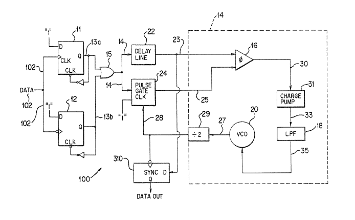
Referring to Figure 3, a block diagram of a
clock recovery system lO0 is illustrated wherein
similar elements are referred to with the same name
and/or reference numerals. A data signal 102 is
input to the clock signal input port (CLK) of a
positive edge detector logic element ll and a
negative edge detector logic element 12. The logic
elements 11, 12 may be D-flip flops. In the FDDI
application, the incoming data signal 102 is a non-
return to 2ero-inverted (NRZI) data signal which may
originate at a remote station (for example 60 miles
away) and be coupled to the clock recovery system 100
via fiber.
Referring also to Figure 6, a constant signal D
is also input to the logic elements 11, 12 and, in
the preferred embodiment, the constant signal D is a
logic high or "1". If a rising (or positive) data
transition 20~ occurs in the data signal 102, during
a particular data cell 200, the positive edge
detector ll generates a positive edge detector output
signal 13a which is a logic high or a "1". With a D-
flip flop, when the signal into the clock input port
transitions, the D-flip flop outputs a signal having
the same logic state as the signal received at the
flip flop's D input port. If a falling (or negative)
data transition 206 occurs in the data signal 102,
the negative edge detector 12 generate a negative
edge detector output signal 13b. If no data
transition 204, 206 is present in the signal 102
during a particular data cell, the flip flops outputs
remain a 0 or a logic low signal. Hence, if a
transition 204, 206 occurs, the corresponding edge
detector output signals 13a, 13b is a logic high
--12--
signal; if no transition occurs, it is a logic low
signal.
The edge detector output signals 13a, 13b are
input to an OR gate 15 and the resulting combined
detector output signal 14 is input to a delay line 22
and also to a pulse gate 24. The delay line 22
delays the combined detector output signal 1~ it
receives by a preselected amount which, in the
preferred embodiment, is the time period of one half
of the synchronization cloc~ period ~the delay is
also equivalent to a VCo clock cycle) and generates a
delayed data signal 23.)
The pximary reason for delaying the combined
detector output signal 14, via the delay line 22,
before it is input to a phase comparator 16 is to
ensure that a sufficient amount of time is available
for the pulse gate 24 to gate in the VCO transition
signal 25 to the phase comparator 16, even if the
data transition 204, 206 occur early or late in the
data cell 200. ~ence, inclusion of a delay line
provides the VCO gating mechanism with sufficient
time to capture or detect the presence of a data
transition, even if the data transition occurs late
in the designated data cell window.
The amount of delay which is appropriate, when a
gat~d VCO configuration is employed, is about one
half of the data cell width. One half a data cell
delay ensures that any data transition that is
expected within a particular cell is captured
regardless of whether it arrives one half a data cell
early or one half a data cell late. It is important
that khe delay line not provide greater than about
one half the data cell width so that the data
transition is not compared with VCO transitions
associated with the adjoininq data cells 200.
3 ~ .3 ~
~eferring to Figures 4 and 5, the delay line 22
may be comprised of a plurality of logic gates 300.
The amount of time that it takes for the edge
detector output signal 13 to propagate through the
logic elements 300 is the time period of the delay.
The preferred VCo 20 is comprised of a plurality o~
inverting logic gates 302, similar to the delay line
gates 300, which feed back on themselves as a ring
oscillator.
The VCO clock cycle is desired to be equal to
the time it takes for a signal to propagate through
the logic gates 302. For example, if the ring
oscillator 20 is comprised of three inverting logic
gates 302, then the VCO clock cycle is e~ual to the
time it would take for the signal to propagate
through six gates 302. A VCO clock cycle is complete
when a signal has propagated once throuqh the ring to
produce a logic 1 state and then propagates through
the ring a second time to produce a logic 0 state.
Hence, the delay line 22 and the VCO 20 are comprised
of elements with equivalent propagation times such
that the delay line 22 delay is about equal to the
time period of the vcO~s 20 clock cycle. The
propagation time of the gates 300, 302 is controlled
by the DC voltage applied to trace 140.
Since the positive edge detector logic element
11 produces a logic one pulse upon receiving a rising
data transition 204 and the negative edge detector
logic element 12 produces a logic one pulse upon
receiving a falling data transition 2n6, either
incoming data transition 204, 206 produces a positive
pulse. The positive pulse produced propagates down
to the delay line 22 to be compared with a VCo
transition signal 25.
The clock recovery system 100 performs well
except when the rising and the falling transitions
-14-
204, 206 occur close together. When the rising and
falling transitions occur too close together, the OR
gate 15 does not see the second signal and results in
the second occurring transition being lost due to
pulse overlap.
Assuming the propagation time for both rising
edge 204 and falling edge 206 signals to be the same,
the delayed data signal 23 is input to a phase locked
loop 14 having the phase comparator 16, the VCO 20,
and a low pass filter 18. The phase locked loop 14
regenerates a continuous clock signal 27 (or VCO
transition signal) by comparing the phase transitions
of the delay~d data signal 23 with the phase
- transitions of the gated clock signal 25 generated by
the VCO 20. When the PLL 14 is locked, the delayed
data signal 23 arrives at the phase comparator :L6 at
approximately the same time that the gated VCO
transition signal 25 arrives.
The clock signal 27 is divided by a divider ~
to generate the VCO transition signal 28. (In the
preferred embodiment, the clock signal 27 is divided ~ IC
by a divide by two divider in order to remove any
duty cycle dissymetries in the clock signal 27
generated by the VCO 20.) The pulse gate 24 gates
off (or blocks) the divided VCO transition signal 28
~rom propagating to the phase comparator 16 if no
data transitions 204, 206 are present in the data
cell 200.
The VCO transition signal 28 is input to the
clock signal port of the pulse gate 24 and is used as
the clock signal. The positive edge detector output
signal 13a is ORed by OR gate 15 with the negative
edge detector output signal 13b and the combined
detector output signal 14 latches a "1" into the
pulse gate 24 if either a positive or negative data
transition 204, 206 is present in the data signal
-15-
102. The combined detector output signal 14 is a
positive pulse if a transition 204, 206 is present;
otherwise it is a logic low.
The VCO transition signal 28 is blocked from the
phase comparator 16 by ~he pulse gate 24 if no data
transition 204, 206 is present in the data signal
102. For this condition, the pulse gate output
signal 25 remains a l~gic zero when the rising edge
of the VCO transition signal 28 occurs. The pulse
gate output signal 25 is a logic low because the
combined detector output signal 14 is a logic low, if
no transition 204, 206 is present in the data signal
102, ef~ectively blocking off the VC0 transition
signal 28 from propagating to the phase comparator
16.
As previously discussed, in serial data
applications, the re~erence signal received by the
system 100 is a data signal 102, and often it is not
known when the rising 204 or falling 206 data
transitions are going to occur in a particular data
cell 200. However, it is known that the data
transitions 204, 206, if they are to occur, occur at
intervals defined to be the data cell spacing. The
data signal 102 may be sampled during the data cell
200 to determine if the data changed states during
the data cell time period. By delaying the combined
detector output si~nal 14 before comparing it with
the gated VCO transition signal 25, and by using the
pulse gate 24 to control the passage of the VCO
transition signal 28 to the phase comparator 16, the
system 100 has enough time to detect the presence of
data transitions 204, 206 before a phase comparison
is made.
The combined detector output signal 14 is input
to the pulse gate 24 at about the same time that the
signal 14 is input to the delay line 22. The
tJ ~
-16-
propagation time through the pulse gate 24 is not
critical because the feedback loop tracks it out.
In theory, the data transitions 204, 206 occur
in the center of the data cell window 200, which, as
previously discussed, is 8 ns wide. However, the
transitions 204,206 of the delayed data signal 23 may
not occur in the center of the data cell window 200
due to a number of mechanisms associated with the
transmitt2r, fiber interface, optica} receiver or
clock recovery delay line. Under ideal conditions
the data transitions 204, 206 and the VCo transitions
28 are assumed to consistently arrive simultaneously
at the phase comparator 16 inputs. If this condition
is stable, then it equates to the data arriving
"centered" in the window of the resynchronizer 310.
The resynchronizer 310 samples the delayed data
signal 23 arrivin~ at the phase comparator 16 using
the D flip-flop 310 clocked off of the inverse phase
edge of the VCO transition signal 28 that is being
used for phase comparisons. Using the inverse VCO
phase edge 28 positions the delayed data transitions
half way between the clocking edges which results in
the maximum setup and hold time (by centering the
data in the data cell window).
The divided VCO signal 28 can be used as a
reference point, for purposes of window centeriny, as
it is the clock source for the synchronizer flip-
flop 310 and its phase transitions do not move
instantaneously from one phase comparison to the next
due to the loop filter 18.
If a data transition 204, 206 occurs between
4 ns. and 8 ns. into the data cell 200, it is
considered late. If for example the data was 4 ns.
late, (and therefore, at the edge of the data cell)
the edge detector output signals 13a, 13b would be
ORed toyether and the combined detector output signal
r~
-17-
14 would be received by the pulse gate 24 with
marginally enough time for 1) the pulse gate 24 to
detect whether a data transition 204, 206 is present
in the signal 14; and 2) whether the VCO transition
signal 28 is permitted to propagate to the phase
comparator 16.
The data transitions 20~, 206 may also occur
almost 4 ns. early in the cell window ~00.
Together, the delay line 22 and the pulse gate
24 accommodate for the early and late arrival of data
transitions within the data cell 200. If data
signal's 102 transitions 204, 206 occur up to 4 ns.
late (i.e.l after the center of the cell window) as
referenced from the transitions in the VCO transition
signal 28, the pulse gate 24 is set by signal 14 to
enable a VCO transition 28 just before the VCO signal
28 arrives at the pulse gate 24 input.
If the data transitions arrive early in the data
window, as referenced from the transitions in the VC0
transition signal 2~, then the pulse gate 24 is set
to enable a VC0 transition 2~ in advance thus
permitting the VCO transition signal 28 to propagate
through, as the gated transition signal 25. The
early edge detector output signal 13a, 13b is delayed
by the delay line 22 prior to baing input to the
phase comparator 16. The delay introduced to the
combined edge detector output signal 14 is such that
the delayed data signal 23 arrives at the phase
comparator 16 ahead of the gated transition signal
25.
Ideally, if consecutive data transition occurs
in the center of the data cell, then the data pulses
appear wide (8 ns.). If consecutive data transitions
are not centered in the data cell 200, (i.e., one
late followed by one early), then a narrow data pulse
results. The clock recovery system 100 may become
-18-
unstable when it was presented with a data pattern
that had one transition several nanoseconds late
followed by a data transition which is several
nanoseconds early. As previously discussed, data
pulse narrowing may cause the system 100 to fail due
to pulse overlapping at OR gate lS.
Referring to Figure 7, another clock recovery
system 50, which accommodates for the narrow pulses
!~ and pulse overlap, is illustrated. The system 50 is
~0~ similar in operation to the system 100 of Fig. 6
except that the data signal 102 propagates directly /-¦~
}~ to the delay line 22. An exclusive NOR gate (XNOR) ~, fi,~
receives the data signal 102 and delayed data ,~
signal 23 and produces a rising transition signal ~.2
if any transition in the signal is present, after the
time specified by the delay line 22. The problem of
pulse overlapping, caused by two transitions 204, 206
occurring close together, is eliminated but requires
the delay line 22 to be capable of receiving a data
signal 102 having narrow data pulses.
Similar to the system 100 of Figure 3, the data
signal lQ2 is input to the clock signal input port
(CLK) of a positive edge detector logic element (F1)
108 which may be a D-flip flop. A constant logic
high signal is input to the data port Dl of the
positive edge detector 108. If a rising edge 204
data transition is received, then the positive edge
detector 108 generates a positive edge detector
output signal (Ql) 109 which is also a logic high
signal since a D-flip flop outputs a signal 109
having the same logic level as the signal input to
its data port Dl.
The positive edge detector output signal 109 is
input to the data port D2 of a positive pulse gate
logic element 124 (F2). The positive pulse gate 124
may also be a D-flip flop which receives at its clock
~ r~ r-
--19--
input port CLK the VCO transition signal 28. On the
rising edge of the VCO transition signal 2g, the
positive pulse gate 12~ generates a positive gated
transition signal 152 (Q2) having the same logic
level as the positive edge detector output signal 109
since, on the rising edge of a clock signal, a D-
flip flop outputs a signal having the same logic
state as the data signal it receives. The positive
gated transition signal 152 is input to the positive
edge detector tmore commonly called a D-flip flop)
108 which clears it when the signal 152 is a logic
high.
The data signal 102 with a falling transition
- is input to the clock signal input port (CLK) of a
negative edge detector logic element 110 (F4). The
negative edge detector 110 may also be a D-flip flop
and also receives a constant logic high signal at its
data input port D4. The negative edge de~ector 110
also generates a logic high negative edge detect,or
output signal 111 (Q4) when a negative edge 206 of
the data signal 102 is received.
~he negative edge output signal 111 is input to
the data port D5 of a negative pulse gate 126 (Q5),
which also i5 a D-flip flop. The VCO transition
signal 28 is also input to the clocX port of the
neqative pulse gate 126 such that, on the rising edge
of the VCO transition signal 28, the negative pulse
gate 126 generate a negative gated transition signal
154 having the same logic level as the negative edge
detector output signal 111 which is input to the
negative pulse gate's data input port D5. The
negative gated transition signal 154 (Q5) is input to
the negative edge detector 110 which clears it when
the negative gated transition signal 154 is a logic
high.
SJ ,!
-20-
Referring also to Figures 6a-6c, a data signal
102 having a rising 204 and a falling 206 transition
is illustrated in Figure 6a. The rising edge 204 is
input to the positive edge detector 108 which outputs
a logic high positive edge detector output signal 109
when the data signal D1 is a logic high signal, as
illustrated in Figure 6b. The positive edge detector
108 generates a wide signal 10~ which stays high
until the positive gated transition signal 152 clears
the positive edge detector 108.
The negative edge 206 of the data signal 102 is
received by the negative edge detector 110 which is
sensitive to falling data transitions. The negative
edge detector llO outputs a logic high negative edge
detector output signal 111. The negative edge
detector output signal 111 remains high until it is
cleared by the negative gated transition signal 154.
Hence, the negative edge detector 110 and the
positive edge detector lQ8 generate signals 111, 109
having wide pulses.
Re~rring again to Figure 7 as previously
discussed, the data signal 102 is also input to the ~ ~'
delay line 22 which delays the data signal 102 by a
preselected amount. The delayed data signal 23 and
the non-delayed data signal 102 are input to the
r~J ; ~ logic element ~ which converts the delayed data
signal 23 into data pulses. The logic element
in the preferred embodiment, is an exclusive NOR gate
. When the two exclusive NOR ~ate inputs 23, 102
are not the same, then the exclusive NOR gate outputs
a 0. The data signal 102, which has both negative
206 and positive 204 data transitions, is converted
into a pulsed data signal 224 which is input to the
phase comparator 16.
The positive and negative transition signals
152, 154 are input to another logic element, which is
.
~ r) 5?~
t. _~1 .h.
-21-
an OR gate (G2) in the preferred embodiment which
generates a gated transition signal 25. The OR gate
G2 generate a logic high gated transition signal 25
if either a rising 204 or a falling 206 data
transition occurred in the data signal 102. The
phase comparator 16 generates the correction signal
30 indicative of the phase discrepancy between the
pulsed data signal 224 and the gated transition
signal 25.
The phase comparator 16 receives the gated
transition signal 25 and the delayed pulsed data
signal 224 within the same clock period and compares
the phase of the two signals 224, 25. When the VCO
20 has achieved lock, the two signals 224, 25 into
15 the phase comparator 16 are phased aligned. If there
is a difference in the phase o~ the two signals, the
phase comparator 16 generates a correction signal 30
having a width that is proportional to the phase
error between the delay line output signal 23 and the
20 gated transition signal 25.
The correction signal 30 is input to a charge
pump 31 circuit which converts the voltage correction
signal 30 into an current correction signal 33. The
current correction signal 33 is filtered by the low
25 pass filter 18 before being input to the VCO 20.
Depending upon the correction signal 30 generated,
the correction signal 30 either charges up or
discharges the charge stored in the lowpass filter's
capacitor 18. The filtered signal 35 is input to the
30 VCO 20 and either increases or decreases its
frequency so that the VCO 20 produces a continuous
clock signal 27 whose rising phase transitions occur
in phase with the delayed pulsed data signal 22~.
It may take a different amount of time for a
35 falling edge transition 206 to propagate through the
delay line 22 than it takes for a rising edge
~ ?~
-22-
transition 204 to propagate through the delay line
22. The dissymetry between the propagation times for
rising and falling data transitions causes the VCO
correction signal 30 to vaxy, due to the delay
dissymetry rather than from a phase discrepancy in
the data signal. In addition, a conventional delay
line 22 is typically designed to receive data signals
having a certain width and has difficulty passing a
signal having a narrower width. In particular, the
delay line cannot pass a data signal narrower than
the propagation time o~ one of its single }nternal
gates. For example, if it takes about 1 ns. for a
signal to propagate through one of the delay line
gates, then the minimum width of the data signal it
can pass is about 1 ns.
Referring to Figures 9 and 10, an edge
transition insensitive de~ay line clock recovery
system 300 which accommodated for the different
propagation delays associated with positive and
negative edge transitions is illustrated in Figure 9
and a corresponding timing diagram is illustrated in
Figure 10. The system 300 receives the data signal
102, in NRZI format, and provides separate but
identical data paths 104, 106 for the signals with
positive data transitions 204 and for the signals
with the negative data transitions 206. The positive
data edge circuitry 104 is dedicated to the positive
data transitions 204 and the negative data edge
circuity 106 is dedicated to negative data
transitions 206.
Separate circuitry is dedicated to the positive
edge transition 204 and negative edge transitions 206
in order to eliminate the introduction of different
propagation times associated with negative edge data
and positive edge data. By having a first delay line
120 dedicated to positive edge data 204 and a second
~ J~
-23-
delay line 122 dedicated to negative edge data 206,
the propagation time dissymetries are accounted for
since both delay lines 120, 122 are presented with
positive going edge transitions.
The separate circuitry 104, 106 also reduces
unnecessary truncation of the data cell time window
because the rising and falling transitions are
captured and released independently (i.e., by
separate circuitry 104, 106). It is possible to push
a pair of rising and falling data transition towards
one another until flip flops 108 and 110 function
incorrectly due to minimum pulse width constraints.
(Pairs of transitions are said to "push to~ard one
another" if one data transition occurs late and the
next data transition occurs early.) Edge triggered
flip-flops require the data to remain stable for a
certain period of time before the clock edge occurs.
Otherwise the flip-flop may function incorrectly.
The positive data edge circuitry 104 is
comprised of a positive edge detector logic element
(Fl) 108 which is sensitive to rising edge data
transitions 204 in the data signal 102 it receives at
its clock pulse input port 116. In the preferred
embodiment the positive edge detector 108 is a D-
flip flop with a Ql output signal 109 and a Ql output
signal 112. Because the positive edge detector 108
is cleared prior to the arrival of the data signal
102, a logic high or a "1l' at the Ql output is fed
back into the positive edge detector's data input
port (Dl). On the rising edge 204 of the data signal
- 102, the positive edge detector 108 generates a
positive edge detector output signal 109 having the
same logic state as the signal 112 it receives at its
data input port Dl.
Thus after initialization, the positive edge
detector output signal 109 will be at a logic low
-24-
before the data signal 102 .i5 received (Figure lOc).
When the positive data transition 204 is received by
the positive edge detector 108 (Figure lOa), the
positive edge detector 108 outputs a positive edge ,~
detector output signal 109 (Figure lOc) having the ( '
same level as the ~r=~ signal 112 it received at
its data input port D1 ~pQl~us3~*q (i.e., the output
``i signal 109 ~ logic high signal (or a "l")).
~;l` The positlve edge detector output signal 109
(hereinafter referred to as "positive data signal")
i is input to a first delay line 120 which delays the
positive data signal 109 by a preselected amount and
t generates a delayed positive data signal 128 (Figure
,"~ a). In the preferred embodiment, the delay
introduced is about equal to a VcO clock period,
which in the preferred embodiment is 4 ns. The speed
of the first delay line 120 is identical to a voltage
controlled oscillator (VC0) 128 since the VC0 128 and
the delay 120 have similar gate architecture and a
common input lead 140 which controls their
propagation delay time (Figures 4 and 5).
The delayed positive data signal 128 is input to
the clock signal input port of a positive edge phase
logic element (F3) 132. The positive phase
comparator system consists of the positive phase
logic element 132, a positive pulse gate 124, and a
logic gate G1. Hence, the positive phase comparator
has two inputs: the delayed positive signal and a
VC0 transition signal 148.
The positive phase logic element 132, in the
preferred embodiment, is also a D flip flop which is
matched in all characteristics (i.e., layout
orientation and power level to a negative edge phase
comparator logic element (F6~ 134). The data input
port D3 of the positive phase logic element 132
receives a constant logic high or "l" data port input
?~
-25-
signal 136 (Fig. 10b) as an input and the positive
phase comparator 132 generates a positive phase
output signal (Q3) 1~4. The positive phase output
signal 14~ is one of the output signals generated by
the positive phase comparator system.
When the delayed positive data signal 128 has a
rising edge 204, (Fig. 10d) then the positive
comparator output signal 144 generated (Fi~. 10g),
also has the same logic level as the signal 136 input
to the data port D3. Hence, the positive comparator
output signal 144 is also a logic high signal. If
the delayed positive edge signal 128 does not have a
rising edge, then this signifies that a positive data
transition 204 did not occur in a particular data
cell 200. Hence, the positive phase logic element
132 records the occurrence of the delayed data signal
128 arriving by ganerating the positive phase output
signal 144.
The positive comparator output signal 144 is
input to a first logic OR (G2) 176 along with a
negative phase output signal 146. (The negative
phase output signal 146 is one of the output signals
generated by the negative phase comparator.) If
either signal 144, 146 is a logic high, then the
first OR gate (G2~ 176 generates a logic high PUMP UP
signal 180 (Fig. 10n). Thus, if a rising edge
transition 204 occurs in the data signal 102, a PUMP
UP signal 180 is generated.
The positive edge detection output signal 109 is
also input to the data input port D2 of a positive
pulse gate logic element (F2) 124, which is a D flip-
flop in the preferred embodiment. A voltage
controlled oscillator (VCO) 128, which is part of the
system's phase locked loop 14, generates a signal 127
to track the frequency of the data signal 102. The
signal 127, in the preferred embodiment, is divided
-26-
by a second preselected amount by a divider 129, (a
divide by two divider in the preferred embodiment).
The divided signal 148 is the VC0 transition signal
148 which is input to the clock signal input ports of
the positive pulse gate logic element 124. The VC0
transition signal 148 clocks in the data signal D2 on
its rising edge and the positive pulse gate generate
a positive pulse gate output signal 152 (Q2) having
the same logic level as the signal 113 into its data
port D2. The positive pulse gate output signal 152
is one of the positive phase comparator system output
signals.
The positive pulse gate 124 controls the
propagation of the VC0 transition signal 148 and by
doing so, it has dual functions. First, the positive
pulse gate 124 records the occurrence of ~he VCo
transition signal 148 only when the positive data
edge circuitry 104 receives a rising edge data
signal. The occurrence o~ the VC0 transitlon signal
148 is recorded only when there is a positive data
transition in the data signal 102 because, in the
preferred embodiment, the positive phase comparator
only compares the phase of the positive data signal
109 and the VC0 transition signal 148 if in fact the
positive data edge circuitry 109 did receive a rising
edge transition signal. Hence, the positive pulse
gate 124 in effect functions to "gate" the VC0
transition signal 148.
The second function of logic element 124 is to
control the commencement of the positive phase
- comparator system by initiating its operative by
recording the occurrence of a VC0 transition by
generating the gated VC0 transition signal 152.
The occurrence of the VC0 transition signal 148
(Figure lOe) is recorded by the positive pulse gate
124 generating a logic high signal (or "1") positive
. f ~
-27-
pulse gate output signal 152 (Figure 10f) when the
positive data signal 109 is a logic high (Fig. lOc).
(Again, the positive data signal 109 is a logic high
when a rising edge 204 data signal 102 is received
(Fig. 10a). If no rising edge 204 occurs in the data
signal 102 during a particular data cell, then the
positive data signal 109 is a loyic low and the
positive pulse gate 124 outputs a logic low positive
pulse gate output signal 152, in effect not
10 acknowledging the presence the VCO transition signal
148, even though the VCo 128 continues to generate a
clock signal 127 which would have been in phase with
the data signal 102 had it occurred.
The positive pulse gate output signal 152 and a
15 negative pulse gate output signal 154 are input to a
second logical OR gate (G3) 178. If either input
signal 152, 154 is a logic high, then the second OR
gate 178 generates a logic high PUMP DOWN signal 182
(Fig. 10o). Hence, if a rising edge transition 204
20 occurs in the data signal 102 during a particular
clock cycle, then a PUMP DOWN signal 182 is also
generated.
The positive pulse gate output signal 152 and
the positive comparator output signal ~44 are input
25 into a first reset circuitry element 184 (G1) which
in the preferred embodiment is a first logical NOR
gate (Gl) 184. The first reset circuitry 184
produces a first reset signal 160 which is input to
the positive pulse gate 124 and the positive phase
30 comparator 132 to clear them after they have both
generated logic output signals 144, 152. The
clearing of the positive pulse gate (F2) 124 and the
positive phase comparator (F3) 132 terminates the
phase comparison sequence by the positive phase
35 comparator system and determines the charge pump
signals 180, 182 minimum pulse widths (Figures 8a-
-28-
8c). Logic signals 144 and 152 directly result in
charge PUMP UP 180 and charge PUMP DOWN 182 signals.
The first signal ~the positive phase comparator
output signal 144 or the positive pulse gate output
signal 152) to arrive that is a logic high turns ON
one of the pump circuits; the second signal to arrive
that is a logic high turns ON the other pump circuit~
The last signal to transition high produces a minimum
width pump pulse.
When the positive pulse gate 124 and the
positive phase comparator 132 receive the first reset
signal 160 (logic high), the positive pulse gate
output signal 152 transitions low as does the
positive phase detector output signal 144. In
addition, the first reset signal 160 also is input to
the positive edge detector 108. When the positive
edge detector 108 receives the logic high reset
signal 160, the positive data signal 109 becomes a
logic low signal. When the positive data transition
204 occurs very late in the data cell window 200, the
clearing of the positive edge detector 108 may in
fact occur during the data clock cycle when the
negative edge detector ~10 receives a negative data
transition 102. The availability of time during the
negative data transition cycle to clear the positive
transition circuitry 104 makes it possible for the
system 100 to handle closely spaced data transitions.
The negative data edge circuity 106 is identical
to the positive data edge circuitry 104, except that
the negative edge detector 110 is sensitive to
falling data transitions 206. The negative data edge
circuitry 106 has a negative edge detector logic
element (F4) 110 which is sensitive to falling edge
data transitions 206 in the incoming data signal 102
it receives at its clock signal input port 118. The
negative edge detector 110 may also be a D flip flop.
r ~ 3 .
--29--
The negative data edge circuitry 106 has a
second delay line 122 which is matched with the first
delay lines 120 in respect to power level and layout
orientation. (ie. both delay lines 120, 122 delay
the data signal it receives by about the same amount
and both of the delay lines 120, 122 are controlled
by the loop filter node 35 as much as the VC0 12
is . )
Like the positive edge detector 108, the
negative edge detector llo is a D flip-flop, in the
preferred embodiment, with a Q4 output signal 114 and
a Q4 output signal 111. Because the negative edge
detector 110 is cleared prior to the arrival of the
data signal 102, a logic high or a ~ ' at the Q4 ~ ¢l
output signal 114 is fed back into the negative edge
detector's data input port D4 ~ i3~q~. When a
falling edge data transition 206 occurs in the data
signal 102 (Fig. lOa), the negative edge detector 110
generates a negative detector output siynal 111
(hereinafter referred to as "negative data signal")
having the same logic level as the signal it receives
at its data input port D4 (Fig. lOi).
The data signals Q1, Q4 input to the edge
detectors 108, 110 cannot be driven from a constant
force 1 level condition due to the possibility of
illegal states upon power up. If a constant force 1
is used instead of feeding back Ql and Q4, then it is
possible on power up for signals 109, 111 to be high
and signals 144, 146 to be low. Thus, the data
signal 102 would be unable to produce a positive
transition at delayed data signals 128, 130 allowing
signals 144, 146 to transition high and clear the
edge detectors lOB, 110.
In the preferred embodiment, if the detectors
108, 110 power up with signals 109, 111 in a high
state, then the data signal 102 causes the detectors
f~ J~.
-30-
108, 110 to toggle to a low state due to the feedback
of Ql and Q4 to inputs D1, D4. Thus the detectors
10~3, 110 are initialized to a logic low state.
The negative data signal 111 is input to the
second delay line 122 which delays the negative data
signal 111 by the preselected amount thereby
producing a delayed negative data si.gnal 130
~Fig. 10j). In the preferred embodiment, the first
and the second delay lines 120, 122 are each
comprised of six non-inverting differential "ECL"
logic gates 300 (Figure 4).
A negative phase comparator system consists of a
negative phase logic element 134, a negative pulse
gate 126 and a logic gate G4. The negative phase
comparator system also has two inputs: the delayed
neAgative data signal 130 and the VCO transition
signal 148.
The delayed negative data signal 130 is input to
the clock signal input port of a negative phase logic
element 134 (F6). In the preferred embodiment, the
negative phase logic element 134 is also a D flip
flop and a constant logic high signal 138 (or "1")
(Fig. 10b) is input to its data input port D6. On
the rising edge of the delayed negative data signal
130, the negative phase logic element 134 generates a
negative phase output signal (Q6) 146 that is the
same level (logic high) as the signal 138 input to
its data input port D6 (Fig. 101). If the delayed
negative data signal 130 does not have a rising edge
during a particular data cell, the negative phase
logic e].ement 134 remains a logic low signal 146.
The negative phase output signal 146 is one of the
output signals generated by the negative phase
comparator system.
The negative data signal 11~ is also input to
the data input port D5 of a negative pulse gate 126
--31--
(F5), which in the preferred embodiment is a D flip-
flop. The VCO transition signal 148 is also input to
the negative pulse gate's 126 clock signal input port
150. Similar to the positive pulse gate 124, the '/ ;.1~ i
negative pulse gate 126 records the occurrence of the~ ~
VCO transition signal (Fig. ;~) when a falling ~,/ /:;t
transition 206 occurs in the data signal 102.
On the rising edge of the VCO transition signal
148, the negative pulse gate 126 generates a negative
pulse gate output signal 154 (Q5) (Fig. 10k) which
has a logic level that is khe same as the logic level
of the negative data signal 111 which is input to the
negative pulse gate's data port D5. The negative
pulse gate output signal is another one of the output
signals generated by the negative phase comparator
systern. Hence, the negative pulse gate output signal
154 is a logic high signal when the negative data
signal 111 is a logic high. The negative data
signal, in turn, is a logic high when the data signal
102 has a falling transition 206.
As with the positive phase comparator system,
the negative pulse gate 126 has dual functions.
First, it records the occurrence of the VCO
transition signal 148 to "gate" it in when a negative
data transition is detected. The second function of
logic element 126 is to control the commencement of
the negative phase comparator system by initiating
its operation by gating the VCO signal 154.
As previously discussed, the negative phase
output signal 146 is input to the first OR gate 176.
When the negative phase output signal 146 is a logic
high ~i.e., a falling data transition was received by
the negative edge detector 110) the first OR gate 176
generates a logic high PUMP UP signal 180 (Fig. 10n).
Similarly, as previously discussed, the negative
pulse gate output signal 154 is input to the second
--32--
OR gate 178; if the negative pulse gate output signal
154 is a logic high signal (i.e., a falliny data
transition 206 occurred), a logic high PUMP DOWN
signal 182 is generated (Fig. 10o).
The negative pulse gate signal 154 and the
negative phase output signal 146 are input to a
second reset circuitry 186 (G4), which, in the
preferred embodiment, is a second logical NOR gate
(G4). The second NOR gate 186 generates a second
reset signal 162 which is used to clear the negative
pulse gate 126 and the negative phase logic element
134, when they have both generated logic high output
signals 146, 154, thereby terminating the operation
of the negative phase comparator system. The NQR
gate 186 is preceded with inverting gates 187
(forming the eguivalent of an AND gate function) to
intentionally introduce an additional gate delay and
gate architecture. The inverting gates 187 set the
minimum charge pump pulse width and minimize the
propagation delay differences of the second reset
circuitry 186 when activated from the negative pulse
gate output signal 154 versus the negative phase
output signal 146.
The PUMP DOWN signal 182 is a negative current
signal and the PUMP UP signal 180 is a positive
current signal which charge down/up a capacitor in
the phase lock loop's low pass filter 18 to
increase/decrease the VCo's 128 voltage and thus to
increase/decrease the VCO's frequency. Hence, the
PUMP UP 180 signal charges up the VCO's capacitor and
the PUMP DOWN signal ~82 discharges the capacitor to
adjust the frequency of the VCO 128 to track the
phase of the data signal 102.
Referring again to Figure 1 and Figures 8a-8c if
the data signal's 102 rising transition 204 is
centered within the clock window and the phase locked
-33-
loop 14 is stable (i.e., the VCO transition signal
148 and the delayed data signal 128, 130 are in
phase) then the positive comparatox output signal
144, is input to the first OR gate 176 at
approximately the same time that the positive pulse
gate output signal 152 is input to the second OR gate
178. The first OR gate 176 ysnerates a PUMP UP
' ~ f~, signal 180 at about the same time that the second OR
gate ~ generate a PUMP DOWN signal 182, thereby
effectively cancelling one another out.
Similarly, if the data signal's 102 falling
transition 206 is centered, then the negative pulse ;/,r~
; gate output signal 154 is input to the first OR gates
j7~ at about the same time that the negative pulce t~ ?
g~ output signal ~æ~ is input to the second OR gate ~i
' ~A - ~ . Again, in this situation, the PUMP UP signal
180 and the PUMP DOWN signal 182 issue approximately
simultaneously.
Referring in particular to Figures 8a-8c, timing
diagrams for the PUMP UP 180 and the PUMP DOWN 182
signals are illustrated. The amount of net loop
correction which results from the occurrence of the
VCO transition signal 127 and the positive and
negative data transitions 204, 206 activating the
PUMP DOWN 182 and PUMP UP 180 signals depends upon
the relative timing between them. Fig. 8a illustrate
the situation when the delayed data transition
signals 128, 130 and the ~ VCO transition ~ "~8
B~ are in phase and arrive at the phase logic
l 30 elements 132, 134~simultaneously. Both the PUMP UP
- 180 and PUMP DOWN signals 182 issue approximately
simultaneously producing PUMP UP 180 and PUMP DOWN
182 pulses of minimum but equal widths (i.e., the
signals 180, 182 last for approximately the same
duration). The charge pump circuitry 31 converts the
PUMP UP and PUMP DOWN pulses 180, 182 into
-34-
complementary polarity currents which are summed at
the filter 18 thereby resulting in a zero net
correction. Hence, the net effect of the PUMP UP
signal 180 and the PUMP DOWN signal 182 on the low
pass filter 18 is about 0.
Figures 8b and 8c illustrate the situation when
either the VCo transition signal 127 or the data
transitions 204, 206 occurs earlier than the other
resulting in the earliest initiatecl pump pulse being
on longar and producing a net non-zero delta
correction to the filter 18. Referring to Figure 8b,
if the delayed data signal 128, 130 arrives at the ,
phase logic elements 132, 134, before the VCO
transition signal 148, ~ then the PUMP UP signal
180 is issued before the PUMP DOWN signal 182 is
issued, and the capacitor in the low pass filter 18
is charged up during the time when the PUMP DOWN
signal 182 is off and the PUMP UP signal 180 is on to
speed up the VCO 128. Again, during the time when
both signals 180, 182 are ON the net effect is ~!,~'
Referring to Figure 8c, if the VCO transition
signal 148 arrives at the phase logic elements -3~a,/~ RA1 /~A'~
$~ before the delayed data signal 128, 130 then the ,.,~_
PUMP DOWN signal 182 is ON before the PUMP UP signal
1~0 is turned on. During the time period when only
the PUMP DOWN signal 182 is ON, the capacitor in the
low pass filter 18 discharges to slow down the VCO
128.
The edge transition insensitive delay line clock
recovery system 300 separately accommodates for the
phase locking of both positive 204 and negative 206
data transitions by having separate circuitry 104,
106 which separates negative transitions 206 from
positive transitions 204 and transforms the negative
data transitions 206 into positive transitions, thus
eliminating delay line propagation delay dissymetries
~?~ f~g~
-35-
due to unmatched propagation times. The delay line
propagation dissymetry is eliminated by the system
300 because negative data transitions 206 are
converted to positive transitions so only positive
data transitions propagate through the negative edge
circuitry delay line 122.
In addition, the system 300 a:Lso addresses the
problem of passing narrow pulses through the delay
lines 120, 122 due to the late and then early arrival
of data transitions 204, 206 in adjacent data cells
200. By having separate data circuitry 104, 106 ~and
therefore separate data paths) for rising 204 and
falling 206 data transitions, the delay lines 120,
122 are presented with a single latched positive data
transition 10~, 111 which remains constant until it
is cleared.
Having thus described the invention, it is
recognized that those skilled in the art may ma]ce
various modifications or additions to the preferred
embodiment chosen to illustrate the invention without
departing from the spirit and scope of the present
contxibution to the art. Accordingly, it is to be
understood that the prosecution sought and to be
afforded hereby should be deemed to extend to the
subject matter claimed and all equivalents thereof
within the scope of the invention.