Note: Descriptions are shown in the official language in which they were submitted.
l 7 ! ~ ~ 9 i
~r. ~:. . , , . i -J
1
Scanning Device
Field of Invention
The present invention is directed to a scanning device
with a waveform generator for supplying a drive signal to
_5 rotate the scanning mirror of a galvanometer,.__or similar type
f device, in a predetermined pattern. The generator provides
a signal with a waveform shape to create a drive signal for
the galvanometer which moves the mirror in a predetermined
pattern with a high degree of precision.
Background of the Invention
Various types of circuitry have been developed to provide
a drive signal to rotate a mirror of a galvanometer to a
required position or the mirror of a light scanning apparatus
in a predetermined pattern. One type of circuit is shown in
U.S. Patent 4,286,212 in which a variable control signal
generator is coupled to input terminals of the galvanometer
through a current amplifier, the angle of the deflection of
the mirror being dependent on the value of the control signal
from the generator. However, due to the fact that the
galvanometer exhibits hysteresis, the deflection angle also
depends to a certain extent on the value of the previously
applied control signal. This hysteresis makes it difficult to
achieve repeatable random access of any particular discrete
angular position of the mirror with great accuracy. In order
to counteract this problem, U.S. Patent 4,286,212 provides a
system to ensure that the control signal applied to the
galvanometer is always returned to a predetermined reference
level for a given period of time before it is changed to a new
value. Therefore, each, new angle to which it is desired to
accurately rotate the mirrar is referenced from substantially
the same reference position to eliminate the effect of
hysteresis on the movement of the mirror.
s~'~ 3., '' .,x -', f; ~;
>.al :: :,,: '~..i .~. ~.J '-.l
U.S. Patent 4,329,011 discloses a laser printer in which
a laser beam is reflected by a galvanometer mirror onto a
recording medium. The drive signals are supplied to the drive
for the mirror from a drive signal generator through a drive
amplifier. The drive signal generator produces a.number of
different voltages which are applied by electronic switches at
particular times in a scanning cycle to the drive amplifier.
These then provide a drive signal which will rotate the .
galvanometer, taking into account the resonant frequency of
the galvanometer, in a manner which will scan the laser beam
across the recording medium at a high and constant speed.
U.S. Patent 4,368,489 describes a system for scanning
frames of potion-picture films including a tilting-mirror
scanning mechanism which deflects the projected image of a
frame across a row of photodiodes, in a direction
perpendicular to the row, periodically at a frequency
corresponding to the vertical scanning frequency of a standard
television picture. The tilting-mirror mechanism employed is
provided with oil-damped action with the damping oil being
maintained at a stabilized temperature by a heating device in
order to provide.a stabilized damping action. The movement of
the tilting-mirror in this device is temperature dependent due
to temperature effects on the damping action of tlae oil.
Other types of scanning devices also have mechanism whose
movements with applied drive signals can vary with changes in
temperature. This U.S. Patent 4,368,489 illustrates the type
of control signal, as well as circuitry for generating the
signal, which will move the tilting-mirror scanning mechanism
with the required scanning sweep.
The above--mentioned references serve to illustrate
various types of mechanism employing rotatable or scanning
mirrors and indicates that the control signals needed for
driving these mirrors vary considerably in the shape of their
waveform depending on the type of mechanism and required
motion. U.S. Patents 4,329,011 and 4,368,489 use pre-encoded
waveforms to generate the desired scanning motion of their
mirrors. These pre-encoded ~aveforms are fixed for any one
.. . n .... ~' j lJ
3
particular type of galvanometer. However, it is impossible to
perfectly predict.the response of any one type of device to a
pre-defined excitation. The motion, as a result can fluctuate
considerably from one device to another for a particular drive
signal waveform and these devices, along with their drive
signal waveform, must then be manually adjusted. The
characteristics of galvanometers or scanning mirror devices
can also change over a period of time due to temperature
changes, aging, drifting etc.
~10 U.S. Patents 4,329,011 and 4,368,489 provide an angular
displacement to their mirrors which is characterized by a,
more or less, sawtooth shape, i.e. a linear rotational motion
of the mirror in one direction followed by a faster return
motion. However, other types of rotational motion of
galvanometers mirrors exist such as sinusoidal rate of
movement. Due to the inertia of the moving mirror and
friction in the system, the voltage waveform required to move
the mirror in a particular manner will not correspond to the
waveform of the actual angular displacement of the mirror.
This is clearly illustrated in LJ.S. Patent 4,648,685 which
show diagrams of the waveforms of voltages applied to drive a
galvanometer mirror and the responsive angular displacements
of the galvanometer mirror in the same figures.
U.S. Patent 4,350,988 shows a system for scanning a laser
beam across a recording medium by moving a mirror which is
driven by a motor so that the angular displacement of the
mirror has a sinusoidal form. A photodetector with a mask
having two parallel slits is positioned so that the laser beam
is reflected towards the detector when it is near one end of
its scan. The detector than provides two pulses and from
these, by measuring the pulse interval, the scanning velocity
at that pos~.tion can be determined. A signal proportional to
the detected velocity and a signal from a reference signal
generator are applied to a comparison circuit which provides
an output signal (error signal) to adjust the speed of the
motor and control the velocity of the beam as it scans the
recording medium.
~
, :. ' !. i
~,.: ...~J .._ '.i S/
S.~mmarv of the Invention
It is an object of the present invention to provide a
scanning device with a drive system to angularly reciprocate a
rotatable element, e.g. the mirror of a galvanometer, in a
desired waveform.
A preferred embodiment of the invention comprises a
scanning device having a drive system to angularly reciprocate
a rotatable element about an axis in a desired waveform,
reference means defining said desired waveform, a programmable
waveform generator for supplying an excitation signal to the
drive system in accordance with said desired waveform, a
position sensor for generating a signal representing the
actual waveform of reciprocation of the rotatable element, and
a microprocessor having (a) means for determining an actual
error signal representing an error between the actual waveform
as determined by the position sensor and the desired waveform
as deterzained by the reference means, (b) means for generating
a model of the scanning device far generating an attempted
error signal, and (c) a waveform optimizer for receiving said
actual error signal and comprising means for obtaining a
difference between the attempted error signal and the actual
error signal to generate a signal representing an imperfection
in the actual error signal, means receiving said imperfection
signal for generating an estimate of the excitation error and
for delivering an excitation correction signal to the waveform
generator to adjust the excitation signal from the waveform
generator to cause the rotatable element to have an actual
waveforan substantially in accordance with the desired
waveform.
Because almost any type of waveform can be programmed and
optimized by the present invention, many types of applications
can be found for the device, such as 3D sensors, laser
printers, photo typesetting, etc.
Brief Description of the Drawings
Figure 1 shows a schematic diagram of a circuit for a
scanning devices according to an embodiment of the present
invention:
s.. ;- r, ,; ::
Figure 2 is a more detailed circuit diagram that
illustrates the function of the system shown in Figure i;
Figure 3 is a schematic diagram of a further scanning
devices according to a second embodiment;
5 Figure 3A shows a side view of a window and photocell
arrangement in the embodiment shown in Figure 3: and
Figures 4A, 4B, 4C, 4D, 5A and 5B show experimental
results obtained with the embodiment of Figures 1 and 2,
Figure 4A being a graph showing an optimized excitation
waveform together with a standard excitation waveform each
division of the graph (T/div.) representing a time of l0 ms,
Figure 4B being a graph showing the response of a galvanometer
to the optimized and standard excitation waveforms shown in
Figure 4A, and Figures 4C and 4D showing related signals
during the optimization process; with Figures 5A and 5B
corresponding to Figures 4A and 4B but in a case in which
each division of the graph (T/div.) represents a time of
2 ms.
Description of the Preferred Embodiments
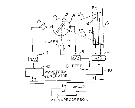
Referring to Figure 1, a galvanometer 1 is driven by
signals from a programmable waveform generator 13, which are
applied through a digital-to-analog converter 14 and a current
amplifier 15. The output of the current amplifier 15 is
applied to drive coils for a mirror 2 of the galvanometer ~..
The drive coils angularly reciprocate the mirror 2 about an
axis, whereby to deflect a laser beam L from a laser 3 so that
this beam scans a surface S between limits L' and L". The
galvanometer 1 has a built-in position sensor 4 which detects
the angular position of the mirror 2. Such built-in position
sensors are standard in the art. See, for example the book
"Laser Beam Scanning: Opto-Mechanical Devices, Systems, and
Data Storage ~ptics by Gerald F. Marshall, published by Marcel
Dekker, Inc. 1985 pp 244-25~, especially section 5.1.2 and
Figure 29 where a capacitive built-in position sensor is shown
just above the lower ball bearing.
The signal from the position sensor 4 is applied to an
analog-to-digital converter 8 whose output is applied through
s9 ;:
6 h ..; ., .~ ~_ .
buffer 10 to a microprocessor 12. The position and movement
of the mirror 2 is determined by the microprocessor 12 from
the signal supplied by the A/D converter 8. The actual
movement (response) of the mirror 2 is thus compared with the
desired response programmed in the microprocessor 12. The
microprocessor 12 can thus determine errors between the actual
response and the desired response to generate correction
signals that need to be applied to the waveform generator 13
in order to adjust the excitation applied to the drive coils
of the galvanometer~l to cause the actual response of the
mirror to correspond closely to the desired response. A clock
generator (not shown) supplies clock signals to the buffer 10,
the microprocessor 12 and the generator 13.
Figure 2 illustrates the system in more detail and its
function. A model 21 of the galvanometer 1 is automatically
built by the microprocessor 12. This model 21 receives the
excitation signal from the waveform generator 13 on line 16
and emits an "attempted" or "model°' error signal on line 19.
The difference between this attempted error signal and the
actual waveform on line 17 is determined by an adder 23 and
fed back to the model 21 on line 18 to constantly update it.
The feedback on line 18 thus serves to adjust the model 21 as
conditions in the galvanometer, such as temperature, vary.
The model 21 could, for example, be an Adaptive Wiener Filter,
such as described in Chapter 7, especially pages 404 to 408,
of the book '°Optimum Signal Processing: An
Introduction°° by
S.J. Orfanidis, MacMillan Publishing Co. 1985.
As more fully explained below, the model 22 is used to
evaluate the excitation correction signal required to be
applied to modify the excitation waveform to compensate for
the errors between the desired response and the actual
response of the mirror 2. The desired response (waveform A in
Figure 4A) is determined by a reference 22 and is subtracted
from the actual response (waveform C in Figure 4B) on lire 25
by an adder 24, to determine the actual error signal E (Figure
4C). This error signal E is applied on line 26 to a wavefarm
optimizer 20 which includes a second model 2I' that is a copy
~ ~i i
7 i..J '.. .. i .- :j -,f
o~ the computer constructed model 21, by which it is kept
constantly updated by signals on line 27. The optimizer 20
also includes an adder 28 that receives the actual error
signal E on line 26, and, by subtracting such signal from the
attempted error signal F (Figure 4C) received from the model
copy 21' on line 29, generates on line 30 a signal G that
represents the imperfection in the actual error signal. This
latter signal G is applied to a further model 31 that
generates an estimate of the excitation error. An excitation
correction signal H from the model 31 is sent on line 32 to
the model copy 21'. Because only this excitation error signal
H is applied to the model 21', the response obtained in signal
F should be equal to the actual error signal of the
galvanometer obtained in signal E. The difference (or
imperfection signal G) between this attempted error signal F
and the actual error signal E is used to modify the estimate
of the excitation error 31, so that signals E 'and F will be
approximately equal to each other. The estimate of the
excitation error (excitation correction signal H) is applied
on lines 33 and 33' to the waveform generator 13. To avoid
instability in the system the line 33 passes through an
accumulator 34 that also receives feedback on line 35 from the
output of the waveform generator 13. This arrangement adjusts
the output of the waveform generator 13 in steps, causing the
system to take a few seconds to start up, but responding
rapidly and accurately after this start up time.
Hence, to summarise, the waveform optimizer 20 applies
the excitation correction signal H to the programmable
waveform generator 13.
Figure 4A shows in waveform A a standard triangular
excitation waveform, in this case the desired excitation
waveform, while Figure 4B shows by waveform C the actual
response of the galvanometer to this standard excitation
waveform A. In other words, when the signal on line 16 is A,
the signal on line 25 is C. The drawing shows that the
waveform C is distorted from the ideal triangular shape A.
Zn order to provide a scan of the mirror 2 that more closely
Sr ~.., i.., y: J, i ~ ~'%
s : ~.; . .. . '.r
follows the desired triangular waveform A, the microprocessor
12 thus employs the circuit shown in Figure 2 to modify the
output from the waveform generator 13 until the desired
waveform A is attained or more nearly attained. The waveform
from the generator 13 that is required to achieve this result
is shown by the waveform B in Figure ~A, and the waveform D in
' Figure 4B shows the response of the galvanometer to the input
excitation signal B. As can be seen, the waveform D is
substantially identical to the desired waveform A, being much
closer thereto than the waveform C was, whereas the necessary
excitation waveform B is substantially different from the
initial excitation waveform A, especially in the regions of
the peaks of the curve.
Thus, by the end of the optimization process the system
tries to obtain a waveform D identical to the waveform A.
Therefore E=A-D will became almost 0, which means that the
estimate of the excitation error will also be almost 0 and
consequently F and G will be almost 0. At the end of the
optimization process E, F, G and H are all close to zero.
The curves for signals E, F, G arid H that are shown in Figures
4C and 4D are thus only valid at the beginning of the
optimization process i.e. when E=A-C rather than A-D.
The time per division in Figure 4 is 10 ms, whereas in
Figure 5 the time per division is 2 ms. Tn other words, the
scanning rate in Figure 5 is fzve times faster than in Figure
4, i.e. 100 Hz, the resonant frequency of the galvanometer
being 70 Hz. In the case of Figure 5B, the galvanometer
response C to the standard triangular excitation A has
deteriorated into a sinusoidal shape. However, the
microprocessor 12 adjusts the output of the wavefarm generator
13 to provide an excitation signal B as shown in Figure 5A.
Although the waveform B differs radically from the desired
scanning response A, it nevertheless results in the actual
response of the galvanometer having the waveform D shown in
Figure 5B which is a close approxa.mation to the desired
scanning response A. With this system for supplying an
optimized excitation drive signal, the scanning speed can be
~
.: ;w. F>. iy
.~ ,~J
~ncreased while the accuracy of the actual response is
substantially maintained.
Errors in the motion of the mirror, other than those due
to inertia, are caused by minute differentials of force
operating on its suspension system and combinations of
magnetomechanical and electronic driver system imbalances that
can vary over a period of time due to temperature changes,
aging, drifts of the electronic components, electrical noise,
hysteresis, dust contamination, etc. Position sensors, such
as the sensor 4 shown in Figure 1, are conventionally
incorporated into galvanometer scanners, but their precision
is limited by the nonlinearity of the position sensor and by
temperature drifts. These will affect both the null position
and the gain of the transducer and, subsequently, the position
of the scan angle. To compensate for these last-mentioned
errors, the galvanometer may also include a photodetector
system such as described in applicant's TJ.S. Patents 4,800,270
and 4,800,271 both issued January 24, 1989. Additional
explanation of this latter system is provided in °'Control of
Low Inertia Galvanometers for High Precision Laser Scanning.
Systems" by F. Hlais, published in Optical Engineering vol 27
No. 2, 104-110 (February 1988). This photodetector system
intercepts at least a portion of the light beam during its
scan and provides synchronizing pulses which are applied to
the microprocessor to more accurately determine the actual
reciprocating motion of the mirror.
In one of the specific systems described in the last-
mentioned patents, two closely spaced photodetectors are
positioned at a location to intercept the beam where the beam
has a large enough cross-section to encompass more than one
photodetector. The beam position is measured by comparing the
amplitudes of the two detected signals as the laser beam scans
the two closely spaced photodetectors, the zero crossing when
the center of the laser beam is at the midpoint of the two .
detectors being determined by a comparator. These two '
photodetectors can be part of an array of many photodetectors
mounted on a single substrate.
r/~~''',,-~f ~x~i
- ~.d ;.~ .~ fi ,._ ~> 'j
In another of the specific systems described in the last-
mentioned patents, the galvanometer can include an inclined
window with two spaced photodetectors located below the
window. This type of system places the photodetectors out of
5 the path of the light beam and is shown in Figure 3 and 3A as
an addition to the system shown in Figures 1 and 2. The laser
beam L reflected from the mirror 2 traverses a window 5 before
it scans the surface S, the window being inclined at an angle
as shown in Figure 3A so that a portion of the laser beam is
10 reflected downwards in the direction of two spaced
photodetectors 6 and 7. In Figure 3A, the photodetector 6 is
not seen because it is located behind the photodetector 7. A
portion of the laser beam reflected by the window 5 intercepts
the photodetectors 6 and 7 as the beam scans the surface S
between the positions indicated by L' and L" in Figure 3.
The photodetector 6 is positioned so that a portion of
the laser beam reflected from the window 5 will intercept this
detector near one end of its scan (L'), while the
photodetector 7 is positioned so that a portion of the laser
beam will intercept the detector 7 near the other end of its ,
scan (L"). As a result, the photodetector 6 will produce a ,
pulse at a time ty, as the laser beam swings towards one end
(L'), and another pulse at a time t2, as the laser beam returns
to swing towards the other end (L"). Similarly, photodetector
7 will produce a pulse at a time t3, as the laser beam swings
towards the other end (L°'), and a further pulse at a time t~,
as the laser beam reverses its scan direction and moves
towards said one end (L').
Assuming that the galvanometer is driven by a sinusoidal
or triangular type of waveform from the generator 13 (sea
Figures 4 and 5), the signals at times t~ to t4 are correction
signals that can be used to determine errors in the scan such
as "Eoffset~~ where the laser beam swings further at one end of
the scan than at the other end, and '°~9a~~" when the laser beam
reflected from mirror 2 swings past the positions indicated by
L' and L" or does not swing far enough to reach these
positions. Another variable that can be determined from the
11 s~. ; -, ..;
o ,''..,', ; ~,t
aignals at times t~ to t4 is the phase shift between ti~ey.actua~ ~~ ~~
scanning motion and the excitation signal waveform for a
sinusoidal drive signal or other simple waveforms. The peak
of one end portion of the laser scan will be at ~ the period
between times t~ and tZ, and the peak at the other end of the
scan will be ~ the period between times t3 and t~. These
features have been described in more detail in the Optical
Engineering article referred to above and also in
Optomechanical Systems Engineering "High precision control of
galvanometer scanner" by F. Blais, Vol. 817, p. 8-16; SPIES
31st Symposium On Optical and OptoElectronic Science and
Engineering, August 16 to 21, 1987, San Diego, U.S.A.
In the embodiment shown in Figures 3 and 3A, the
correction signals at times t1 to t4 are also applied to the
microprocessor 12 through the buffer IO after being converted
into digital form by an A/D converter 9. The microprocessor
12 uses the combination of the signals from the A/D converters.
8 and 9 not only to achieve the improvements demonstrated in
Figures 4 and 5, but simultaneously to determine the actual
position and movement of the scanning laser beam more
accurately. It will be appreciated that there is no conflict
between the two sets of correction signals. The function of
the waveform optimi2er 20 in the microprocessar 12 in Figure 3
remains the same as has been described above in connection
with Figure 2 and relates essentially to shaping the
excitation waveform to achieve the desired response. The
correction signals frown the A/D converter 9 are not concerned
with waveform shape, but act to instruct the system to
correctly control the amplitude, center point and phase of the
oscillation of the mirror 2.