Note: Descriptions are shown in the official language in which they were submitted.
3 ~3 ~
--1--
BACKGROUND OF THE INVENTION
Field of Use
The present invention relates to macrocells and
more particularly to flip-flop cells with a scan
capability.
Prior Art
A well known technique for implementing very large
scale integration (VLSI) microprocessor chips is through
the use of macro or library cells. The logic designer
combines macro cells included in the library
corresponding to types of restricted function building
blocks (e.g. inverters, flip-flops, selectors) by
specifying interconnections between cell inputs and
outputs. The patterns of interconnections are included
in an interconnection layer of the VLSI microprocessor
chip.
In general, the cell/gate array manufacturers
specify a set of design rules which must be followed
precisely in making such interconnections. One such
rule is that there can be no gated clock sign~ls uscd
with synchronous flip-flops. This becomes a problem in
implementing those designs which have registers which
are loaded only on selected conditions. That is, the
register contents do not change on every clock or on
every cycle or on every instruction.
Characteristically, LSI chips often or sometimes
include some type of diagnostic serial scan capability
used in t~sting and verifying proper system operation.
An example of this type of capability is described in
U.S. Patent Nos. 3,582,902 and 4,649,539.
In order to implement such a capability using
v)
--2--
predefined cells, it becomes necessary to interconnect
two or more such cells together. For example, it has
been proposed to connect a scannable D flip-flop and an
input multiplexer cell with another input multiplexer
cell positioned before the input multiplexer to
accommodate the scan requirement. Also, it has been
proposed to interconnect separate inverter, AND/OR and D
flip-flop cells together. Alternatively, the scan
requirement has been implemented by utilizing a special
diagnostic circuit included within a ma~or cell such as
in the arrangement described in U.S. Patent No.
4,575,674.
The above arrangements require additional cells or
space for additional interconnects which not only reduce
chip area but because of longer signal propagation
times, circuit speed is reduced thereby adversely
affecting system performance. Additionally, the use of
different cells can provide different speeds which vary
as a function of the physical locations of the cells
within the array. This can lead to less predictable
operation and difficulties in processing system
conditions.
Accordingly, it is a primary object of the present
invention to provide a device which complies with the
restrictions imposed by IC manufacturers.
It is further object of the present invention to
provide a device which is capable of performing a wide
variety of functions but without requiring an increase
in area when implemented in an macrocell array.
It is still a further object of the invention to
provide a device which requires a minimum signal
propagation delay~
~;J,j '3i~
--3--
SUMMARY O~ THE INV~NTION
The above objects and advantages are achieved in a
preferred em~odiment of the present invention by a
synchronous latch device which is implemented in the
form of a single macrocell of a macrocell array. For
the purposes of the invention, a macrocell is an
extension of the gate array in which macro functions
used to define logic simulations are directly
implemented within the basic cell structure rather than
formed by interconnecting several logic gate cells of a
gate array.
According to the preferred embodiment of the
present invention, the synchronous latch device includes
an input gate section and a scannable latch section.
The input gate section directly connects internally to
the data input terminal of the latch section to provide
a non-inverting path for input data signals. The
non-inverting output terminal of the latch section is
connected to an output pin to provide a signal
representative of the state of the latch for use as a
recirculation or hold input to the latch section.
The input gate section is constructed from a
standard multiplexer part and has a minimum of input
pins. These are first and second complementary
controlled data input pins and a load control input
pin. The load control input pin is normally connected
to a qualifier signal or to other logic circuits within
the system for processing several logic conditions which
are enabled by such qualifier signal.
According to the present invention, either the
first or second data input pins can be interconnected to
the latch output pin for holding the latch in the same
L ~ I ? ~
~, J ~. ~J l
--4--
state to allow for either negative or positive loyic.
That is, the load control or hold function can be
controlled by the load control pin with either negative
or positive logic whichever connection is required for
attaining maximum speed or for minimizing space
requirements.
In operation, the latch device can be conditioned
to store new data or remain in its current state as a
function of the state of the single input signal applied
to its load control input pin in response to positive
going edges of the clocking signals applied to a chip
clock input of the latch device.
In the preferred embodiment, use of a qualifier
signal as part or all of the load control signal
generation function simplifies the way of handling a
variety of control logic functions which require the
selective loadiny of register devices under certain
conditions while still meeting design rule requirements
of having no gated clock control signals. The
arrangement of having two data input pins available for
new data permits the use of the faster hold signal as
the data input thereby minimizing switching time.
During scan operations, no clocking signals are
applied to the chip clock input of the latch device
thereby effectively disconnecting the input section from
the latch section. When so disconnected, clocking
signals are applied to the scan input clock pins of the
latch device for loading the data signals applied to a
scan data input pin of the latch section of the device.
Clearinq is accomplished by forcing the scan data input
pin to an inactive or binary ZERO state. The latch
device of the present invention makes use of standard
macrocells to the extent possible thereby eliminating
~ J~ 3
-5-
the need for additional layers of metalization. Thelatch device of the preferred embodiment requires an
area which is not that much larger than the standard
scannable D flip-flop macrocell, a part of which it
incorporates.
From the above, it is seen how the latch device of
the present invention reduces the complexity and
enhances the speed at which a variety of different
logical functions may be performed. These and other
objects and advantages of the present invention will be
better understood from the following detailed
description when taken in connection with the
accompanying drawings.
BRIEF DESCRIPTION OF THE DRAWINGS
i5 Figure 1 is a block diagram of a preferred
embodiment of the latch device of the present invention.
Figure 2 is a circuit diagram of the latch device
of Fiqure 1.
Figure 3 is a diagram of the layout of a macrocell
array which includes the latch device of the present
invention.
Figures 4a through 4h show different configurations
of the latch device of Figure 1.
Figures 5a through 5d are timing diagrams used in
explaining the operation of the latch device of the
present invention.
DETAILED DESCRIPTION OF THE PREFERRED EMBODIMENT
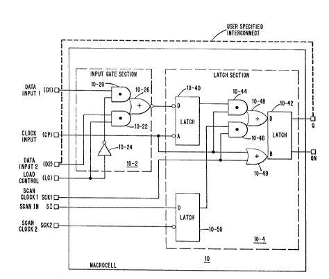
Figure 1 shows in logic diagram form, a latch
device constructed according to the principles of the
present invention. As seen from Figure 1, the device 10
includes an input gate section 10-2 and a latch section
10-4. The input gate section 10-2 is constructed from
an inverting multiplexer which includes a pair of input
AND gates 10-20 and 10-22, an inverter circuit 10-24 and
an output NO~ gate 20-26 which are connected as shown.
The multiplexer may take the form of the standard
inverting multiplexer macrocell part designated as
MUX21L manufactured by LSI logic Corporation.
As shown in Figure 1, the input gate section 10-2
connects directly to latch section 10-4. More
specifically, the output of NOR gate 20-26 connects to
the data input (D) of latch section 10-4. The latch
section 10-4 includes a pair of series connected latches
10-40 and 10-42 and associated input AND gates and OR
gates 10-44 through 10-48 which are connected to form a
synchronous D type flip-flop. The bubble symbol at the
input to latch 10-40 is included to indicate that the
latch device provides a non-inverting path for data
input signals (i.e., there is no inversion of the data
input signals relative to the state of the latch section
10-4 output Q). Latch section 10-4 further includes an
input scan latch 10-50 whose output connects to the data
input of output latch 10-42 through AND gate 10-46 and
OR gate 10-48. Portions of latch section 10-4 may take
the form of the standard D flip-flop macrocell
designated as FDlS2 manufactured by LSI Logic
Corporation.
As shown in Figure 1, input gate section 10-2
connects to a pair of complementary controlled data
input pins, Dl and D2, either of which connect to a data
source or to an output pin Q of latch section 10-4. As
discussed herPin, the connection between the Q output
pin and one of the data input pins D1 or D2 is
externally made through user specified interconnect or
etch. According to the present invention, external
connection to one of the data input pins D1 or D2 is
made as a function of which connection provides faster
operation (i.e., positive or negative iogic). That is,
as explained herein, the connection made is selected
which corresponds to which one of the AND gates 1~-20 or
10-22 responds earlier in time as viewed from the input
during source, such as the logic circuit which is to be
connected to the latch device.
The load control signal which is generated as a
function of one of a number of qualifier signals, Q60 or
Q120, as discussed herein, is applied as the input to a
load control input pin, LC. A chip clock signal is
applied to a clock input pin CP and for switching the
state of the latch device to the state of the data
signal applied to its D input pin.
The latch section 10-4 connects to a scan input
pin, SI and scan clock pins SCK1 and SCK2 as shown.
These inputs are used during system scan mode operations
in which the data output received from a previous latch
device is to be shifted through latch device 10 in a
well known manner under the control of clocking signals
applied to clock pins SCKl and SCK2. The use of two
scan clock pins guards against race conditions.
DESCRIPTION OF FIGURE 2
Figure 2 indicates the specific transistor circuits
used to construct latch device 10. It will be seen that
the gates 10-20 and 10-22 consist of pairs of CMOS
transistors 10-200 and 10-220 whose outputs are wired
j",j, J ~ s~ ~3
O~ed together at node 10-250 and two inverters 10-240
and 10-260. the node 10-250 and inverter 10-260 are
represented in Figure 1 by NOR gate 10-26. The output
of inverter 10-260 directly connects to the gates of
transistor pair 10-402 as shown. The integration of the
gating requirements into the latch device 10 eliminates
the need for inverting buffer circuits thereby
minimizing space requirements and increasing speed by
reducing signal propagation delays. This makes it
possible to utilize an inverter multiplexer macrocell
which requires less area than a non-inverter multiplexer
macrocell.
Latch 10~40 consists of the pairs of CMOS
transistors 10-400 and 10-402 and inverters 10-404 and
10-406 connected as shown. The gates 10-44 and 10-46
consist of the pairs of CMOS transistors 10-440 and
10-460. The outputs of these transistors are wired ORed
at node 10-48 together represented in Figure 1 by OR
gate 10-480 and applied to inverter 10-480. The latch
10-4Z consists of CMOS transistor 10-420 and inverters
10-422 through 10-426 connected as shown. The OR gate
10-49 consists of CMOS transistors 10-490.
The scan latch 10-50 consists of the CMOS
transistor pairs 10-500 and 10-502 and inverters 10-506
and 10-508 connected as shown. Additionally, latch
device 10 includes inverters 10-600 through 10-606 which
are used to generate clock signals ~ F, SCXl and SCX2
in response to signals CP, SCX1 and SCX2 applied to the
corresponding input pins of device 10.
~ 6~,~5
_9_
DESCRIPTION OF FIGURE 3
The preferred embodiment of latch device 10 is
included within a macrocell array, such as the array 100
of Figure 3. The gate array takes the form of the
LCA10129 gate array manufactured by LSI Logic
Corporation. The gate array has a plurality of I/O pads
120, the majority of which are used for logic signals
and remaining used for power and ground.
As shown, a portion of array 100 includes three
latch device macro cells 10a through 10c and a number of
logic macrocells 12. The logic macro cells are
elementary logic gates constructed with 2 to 50 CMOS
transistors. The array can be viewed as a sea of
transistors or gates that are interconnected with
conductive wires. The latch device 10 utilizes a
minimum number of transistors and hence is not much
larger than the area occupied by a scannable standard
D-type flip-flop macrocell.
The macrocells 12 contain different control
structures, portions of which correspond to those gating
structures shown in Figures 4c and 4d. The control
structures of cells 12 combine various sets of logic
conditions corresponding to the logic signals applied to
I/O pad or from other cells with one of two qualifi~r
signals, Q60 and Q120 applied to I/O pads to produce
resulting control signals. The control signals are
routed through a routing area corresponding to the space
or area assigned between cell blocks for
interconnections. Each control signal is then applied
to the load control input pin LC of a different one of
the latch devices 10a and 10b as shown in Figure 3.
Additionally, according to the present invention,
the output pin of latch device 10 of array 100 can be
~Jl ,33''~
--10--
routed to connect to one of the input pins Dl and D2
which is selected so as to maximize speed as explained
herein. In Figure 3, it is assumed that thc latch
devices 10a, 10b and 10c are so connected. In certain
instances, it may be only necessary to apply the
qualifier signal Q60 or Q120 directly to the load
control input pin LC of latch device 10, such as through
an I/O pad as in the case of latch device 10c. Also,
input pin LC can also be connected to a fixed logic
level in the same manner. Additionally, each latch
device 10 can be interconnected to other latch devices
as shown by dotted lines in Figure 3 to provide a scan
capability.
DESCRIPTION OF FIGURES 4a THROUGH 4d
15 It will be obvious to those skilled in the art that
there are a substantial number of different control
structures which are constructed from the elementary
logic gates contained within various macrocells.
Figures 4a through 4d show several examples of control
structures which may be used.
Figure 4a shows an arrangement in which the
qualifier signal Q60 connects to the LC pin of latch
device 10, such as macrocell latch device 10c of Figure
3. The latch or flip-flop 10 will maintain or hold its
present state as long as signal Q60 remains active or
high. Device 10 only changes state or is loaded with
the new data applied to data input pin D1 when signal
Q60 changes to an inactive or low state and upon the
positive going edge of the clock signal applied to clock
input pin CP. The operation is the same when qualifier
signal Q120 is used in place signal Q60.
Figure 4b shows an arrangement in which the
qualifier signal Q60 connects to the LC pin of latch
~? ~ ~ ~
.i t.~ 3 .~J
device 10. The latch device 10 will maintain or hold
its present state as long as signal Q60 remains inactive
or low. Again, device 10 is loaded with the data
applied to pin D2 when signal Q60 switched to an active
S or high state and upon the positive going edge of the
clock signal applied to pin CP.
Figure 4c shows an arrangement in which qualifier
signal Q60 is used in conjunction with several logic
conditions represented by signals control 1 and control
2. This arrangement corresponds to macrocell latch
device lOa of Figure 3. The latch device 10 will
maintain or hold its present state as long as signal Q60
or signals control 1 and control 2 are in an active or
high state. As soon as signal Q60 and one of the
signals control 1 and control 2 switches to an inactive
or low state, device 10 is loaded with the new data
applied to pin D2 when clocked.
Figure 4d shows a similar logic structural
arrangement with the difference that the signal Q60 and
signals control 1 and 2 are applied to pin LC while the
new data is applied to pin Dl. This arrangement
corresponds to the macrocell latch device lOc of Figure
3. In this case, the latch device 10 will maintain or
hold its present state as long as signal Q60 or signals
control 1 and control 2 are in an active or high state.
As soon as signal Q60 and both of the signals control 1
and 2 switches to an inactive or low state, the new data
applied to pin Dl is loaded into the device when
clocked.
From Figures 4c and 4d illustrate the important
feature of the present invention of allowing for the use
of either positive or negative logic which provides
advantages in terms of space or speed. This is
-12-
particularly important in macrocell array chip designs.
The different macrocells have different propagation
delay times for different input loadings when their
inputs are driven from low to high (TPLH) and from high
S to low (TPLH). Thus, the interconnection of the output
pin of each latch device lO can ~e selected so as to be
driven to its reset state by either negative or positive
logic circuits according to which produces the shorter
calculated propagation delay. For further information
regarding the calculation of such delays, reference may
be made to the publication entitled, "The HCMOS
Compacted Array Products Databook" by LSI Logic
Corporation, Copyright 1987.
The remaining Figures show additional arrangements
which allow the use of negative or positive logic
selected as a function of speed. Figures 4e and 4f show
how a synchronous clear function can be included in
latch device lO with a clear signal of either polarity
by reversing the data and ground connections to pins Dl
and D2 as shown. Figures 4g and 4h show how a preset
function can be included in latch device 10 in a similar
manner.
DESCRIPTION OF FIGURES 5a THROUGH 5d
Figures Sa through 5d show how the latch device lO
can be used to perform a variety of functions. Figure
5a shows the basic timing of a processing unit in which
device 10 is used for register storage. The system
clock signal $CLK defines the basic timing for the
processing unit and this signal coincides with the
timing of chip clock signal CP which is applied to the
pin CP of each latch device of the system. The
r
~ L~.jJ~
-13-
qualifier signal Q60 defines the first half of the
processing unit cycle while qualifier signal Q120
defines the second half of the same cycle.
With reference to Figure 4a, it is seen that the
latch device 10 changes state at time 120 while the
latch device 10 of Figure 4b changes state at ti~e 60.
By using qualifier signals Q60 and Q120, the syste~ can
evaluate logic conditions and load the results of these
conditions at times defined by the qualifier signals Q60
and Q120 as shown. Figures 4c and 4d illustrate that
these conditions can be expressed in terms of either
negative or positive logic for selecting whichever is
faster in terms of generating a load control signal
applied to pin LC for loading latch device 10 with new
data.
Figures 5b through 5d shows the timing and the
state of the input signals applied to latch device 10
when the system is operated in a scan mode. Figure 5~
shows the states of the signals for setting all of the
devices 10 within the scan path of the processing unit
to an active or high state. A portion of the scan path
is represented by the dotted lines interconnecting latch
devices lOa, lOb and lOc in Figure 3. Setting is
accomplished by forcing the chip clock CP of each device
to an inactive state. This logically disconnects
input qate section 10-2 of each latch device from the
rest of the device 10. At the same time, the scan data
pin SI of each device 10 is forced to an active or high
state and this state is loaded into each of the devices
in response to the clocking signals applied to input
pins SCKl and SCK2. This mode of operation would
normally ta~e place as part of the power up test
procedure.
-14-
Figure 5c shows states of the input signals for
clearing all of the devices 10 within the scan path to
an inactive or low state. Again, the low state of clock
siqnal CP logically disconnects section 10-2 of each
device lO while pin SI is forced to an inactive or low
state which clears to ZEROS all of the devices 10 within
the scan path. Figure Sd shows the states of the input
signals for loading a scan pattern of "101" into the
scan path latch devices 10.
From the above, it is seen how the latch device of
the present invention can be used to perform a variety
of functions with a minimum of complexity in terms of
the numbers of transistors and gates minimizing area and
at very high speed. The latch device arrangement of the
lS present invention, when used in conjunction with one or
more qualifier signals, can be connected to numerous
types of logic structures so as to enable the processing
of logical conditions with a minimum of propagation
delays. This becomes particularly important when the
device is implemented in a gate array macrocell form.
Many changes may be made to the latch device of the
present invention without departing from its teachings.
For example, the latch device of the present invention
is not limited to the construction or characteristics of
a particular gate array macrocell arrangement or
technology. For example, the latch device of the
present invention may be used in MSI or LSI technology.
Further, it can be used or controlled by any type of
logic structure or directly controlled by means of fixed
voltage signals. Other changes will be obvious to those
skilled in the art.
While in accordance with the provisions and
statutes there has been illustrated and described the
ut~
best form of the invention, certain changes may be madc
without departing from the spirit of the invention as
set forth in the appended claims and that in some cases,
certain features of the invention may be used to
advantage without a corresponding use of other features.
What is claimed is: