Note: Descriptions are shown in the official language in which they were submitted.
~~c~~~~~.
DOCKET R4453.01
EAO:cjf
1 ARRAY ANTENNA WITH FORCED EXCITATION
2 BACKGROUND OF THE INVENTION
3 The present invention relates to antennas
4 for radiating and receiving electromagnetic signals
and, in particular, to array antennas adapted for use
6 on aircraft.
7 DESCRIPTION OF RELATED ART
8 Identification Friend or Foe ("IFF")
9 systems operating with signals of wavelengths in the
range of one foot, for example, are widely used to
11 permit aircraft to transmit and receive IFF signals
12 for aircraft identificaton. Antennas used to radiate
13 and receive IFF signals are commonly mounted on the
1.4 outer surface of fighter and other aircraft, typically,
requiring antennas with a height (dimension out from
lE the surface) of approximately three inches, or about a
17 quarter wavelegth. Fig. la shows a side view of a
18 prior-art antenna, called a "blade" in view of its
19 narrow dimension perpendicular to the page, which is
typically a quarter wave monopole with an associated
- 1 -
~~~~~ a~
1 protective cover. One or rnore antennas protruding
2 three inches from fuselage surfaces of high speed
3 aircraft have obvious undesirable attributes,
4 including creation of drag, limitation of pilo't's
visibility, exposure to fracture during airborne
6 refueling, etc. In addition, prior antennas have
7 typically been nearly omnidirectional, providing
8 little antenna directional discriminatian,
9 Monopole, dipole and slot antennas may be
used 'For these purposes and while there is an
11 extensive body of prior art relating to such antennas,
12 the undesirable features such as antenna height and
13 limited directivity have persisted. Use of monopoles
14 substantially shorter than a quarter wavelength would
alleviate physical disadvantages, but shortening a
16 monopole tends to undesirably affect its electrical
17 characteristics. The prior art encompasses the use of
18 quarter wave sections, also called quarter wave
19 transformers, in antenna applications and the use of
tuning circuits to change or broaden 'the useable
21 bandwidth. Nevertheless) the continuing use of
22 «ircraft antennas of height approximately a quarter
23 wavelength, with omnidirectional or low antenna gain
24 pattern characteristics, testifies to the absence in
the prior art of a satisfactory solution of the
26 problem of providing low drag, low visibility, impact
27 resistant antennas suitable for applications like IF~F
_ 2 _
1 systems and having improved antenna gain and
2 directional characteristics.
3 The present inventor has developed
4 antennas with excitation arrangernents enabling
significant reductions in antenna height and improved
6 antenna patterns. For purposes of comparison with
7 prior antennas, Fig. lb shows the approximate
8 profile and dimensions of an antenna which will be
9 described in accordance with the present invention.
comparative antenna radiation patterns are shown to
11 the right in Fig. 1 and the significantly improved
12 directional pattern shown in Fig. lb for the present
13 invention will be described further.
14 SUMMARY OF THE
INVENTION
I n accordance the present invention,
with
17 an arrayantenna includesterminal means 'For coupling
18 signals and a plurality antenna elements comprising
of
19 at leastfirst, second third antenna elements
and for
couplingradiated signals.First excitation means,
21 coupled between the terminal rneans and the first
and
22 third ements, comprisessignal transmission means
el for
23 couplingsignal componentsof predetermined relative
- 3 -
1 phase and amplitude to the elements by way of a paint
2 of common voltage. Second excitation means, coupled
3 between the terminal means and the second elernent,
4 comprises means for coupling to the second elernent a
signal component ofpredetermined phase and amplitude
6 relative to the signal components coupled to the
7 first and third elements; and the antenna further
8 has tuningmeans coupled to the common voltage point
9 for providing impedance matching. In operation,
signal components in the antenna elements are caused
11 to have a predetermined relationship of phase and
12 amplitude, substantially independently of
13 intercoupling affecting antenna elements of the array.
14 A low-profile array antenna suitable for
aircraft installation in accordance with the invention
16 includes a connector for coupling signals and a first
17 planar conductor pattern providing first, second and
18 third monopole antenna elements each less than
19 one-eight wavelength in height. A second planar
conductor pattern includes first excitation means far
21 coupling the connector to the First and third elements
22 by way of quarter wavelength transformers, second
23 excitation means for coupling the connector to the
24 second element, and tuning means for providing double
tuning in a desired frequency range. The antenna also
26 includes a protective cover of radiation transmissive
27 material and a base member, having a reflective
- 4 -
l .~
1 surface, which enclose and ~;upport the other antennas
2 elements. The entire antenna can be about a tenth of
3 a wavelength high and less than one wavelength long,
4 exclusive of the connector protruding downward from
the base, so that it is suited for aircraft
6 installation with reduced visual and air flow
7 interference.
8 For a better understanding of the present
9 invention, together with other and further objects,
reference is made to the following description, taken
11 in conjunction with the accompanying drawings, and its
12 scope will be pointed out in the appended claims.
13 BRIEF DESCRIPTION OF THE DRAWINGS
14 Fig. I compares a prior art antenna size
and pattern with those of an antenna in accordance
16 with the invention.
17 Fig. 2 shows orthogonal and simplified
I8 exploded views of an array antenna in accordance with
I9 the invention.
Fig. 3 is a plan view showing an arrangement of
21 five Fig. 2 array antennas.
22 Fig. 4 is a block diagram of an array
23 antenna in accordance with the invention.
24 Fig. 5 shows desirable current
relationships for an end-fire array.
_ 5 _
~~~~~c'~~.~
1 Fig. 6 is a circuit diagram ofi a 'three
2 monopole ray antenna in accordance with the
ar
3 invention.
4 Fig. 7 and 8 are circuit diagrams of
alternativeforms of the Fig. 6 antenna.
6 Fig. 9 is an antenna pattern for operation
7 of an arrayantenna of the type shown in Fig.
6.
8 Fig. 10 illustrates component parts of
an
9 array antenna of the type shown in Fig. 6.
Fig. 11 is a circuit diagram of a three
11 slot array antenna in accordance with the invention.
12 Fig. 12 and 13 axe circuit diagrams of
13 alternativeforms of the Fig. 11 antenna.
14 Fig. 14 is a circuit diagram of a five
monopole ray antenna in accordance with the
ar
16 invention.
17 DETAILED DESCRIPTION OF THE INVENTION
18 Referring now to Fig. 2, there is shown
19 the physical configuration of an array antenna 10 in
accordance with the invention. Fig. 2a is an
21 orthogonal view of the complete antenna .including
22 protective cover 12, of a radiation transmissive
23 material such as fiberglass or a suitable plastic,
24 base member 14, of metal or suitable conductive
material to serve as a mounting flange and ground
_ 6 _
J ~ ~ el .~
1 plane connection, and terminal rneans 16, shown as a
2 coaxial connector suitable far coupling RF signals.
3 Fig. 2b and c are exploded end and
4 side views, respectively, of the array antenna 10,
showing cover 12 and base member 14 with connector 16
6 attached. Also shown are a first printed circuit
7 card 18 bearing a first planar conductor pattern of
8 forward, middle and rear monapole antenna elements 20,
9 22 and 24, respectively, and a second printed circuit
card 26 beaxing a second planar conductor pattern on
11 surface 28. The conductor pattern on surface 28,
12 which is not visible in 'these views, will be described
13 below.
14 Tn a specific embodiment of the antenna
lU, the assembled combination of the cover 12 and base
16 14 had a height of approximately one-tenth wavelength
17 and length of about 'three-quarter wavelength.
18 References to dimensions measured in wavelength refer
19 to approximately the average design frequency, so 'that
for a design frequency range or bandwidth of 1,020 to
21 1,100 MHz, for example, the average design 'frequency
22 would be l,060 MHz, corresponding to a waveldngth of
23 about 11.1 inches. Dimensions are stated iri order to
24 characterize the invention and differentiate over
prior art antennas, and are not intended to suggest
26 that the invention is limited to precise dimensions or
27 exclude antennas representing appropriate applications
-- 7 -
1 of the invention. As shown in Fig. 2, the lower
2 surface of base member 14 is Flat, but in other
3 embodiments it rnay be a curved surface corresponding
4 to the curved surface of an aircraft to which it is to
be mounted. For rnounting, screws are typically
6 fastened through the mounting holes shown in Fig. 2a
7 and a clearance hole through the outer surface of the
8 aircraft is provided for the connector 16, so that it
9 can be joined to a mating connector for coupling
signals to cabling and signal processing equipment
11 carried within the aircraft.
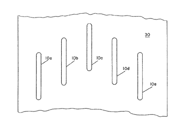
12 Fig. 3 shows a typical antenna system
13 including five array antennas 10a, b, c, d, and a
14 supported in a laterally spaced configuration on a
curved metal surface 30 such as the 'Fuselage of an
16 aircraft, forward of the pilots' windshield. It will
17 be apparent that in such an installation, use of array
18 antennas one inch in height provides a dramatic
19 improvement in the pilot's visibility, as compared to
use of prior art antennas three inches in height. In
21 an installation of this 'type, the individual array
22 antennas can be excited in groupings selected to
23 provide desired antenna beam characteristics, in
24 accordance with known principles of array antenna
excitation. An antenna system as shown in Fig. 3,
26 when installed on the upper forward surface of an
27 aircraft, can provide broad horizontal coverage
_ g _
1 forward of the aircraft and good vertical caverage,
2 except below the aircraft. A similar antenna system
3 installed on the lower forward surface of the aircraft
4 would permit full vertical and horizontal coverage
forward of the aircraft. Alternatively, antenna
6 systems mounted near the leading edge of the wing
7 could provide complete vertical coverage, but would
8 probably require similar systems on the other wing in
9 order to provide complete horizontal coverage free of
blockage by the nose of the aircraft.
11 Fig. 4 is a simplified block diagram of an
12 array antenna in accordance with the invention, shown
13 in two sections 18a and 26a corresponding basically to
14 the printed circuit cards 18 and 26 in Fig. 2. The
antenna is used to alternatively radiate and receive
16 signals, in the range of 1,020 MHz to 1,100 MHz, which
17 are coupled to and from the antenna by way of the
18 terminal means 16a corresponding to connector 16 in
19 Fig. 2. The cover and base components, 12 and 14, are
not represented in Fig. 4. As noted, the antenna is
21 used both to radiate and receive signals, and
22 description of how signals are processed by various
23 portions of 'the antenna when radiating, for example,
24 will be understood to be equally relevant in a reverse
relationship during reception.
- 9 -
2~~~~a.~.
1 The Fig. 4 antenna ine.ludes first, second
2 and third antenna elements 20, 22 and 24, which in
3 accordance with the invention rnay be rnonopoles of the
4 order of one-tenth wavelength in height arranged in a
spaced linear array. While the desirability of using
6 antenna elements one-tenth wavelength high as compared
7 to prior art elements one-quarter wavelength high rnay
8 be readily apparent, the severe operational bandwidth
9 degradation normally associated with short antenna
elements such as monopoles has been a limiting Factor
11 contributing to the continuing reliance on quarter
12 wave elements in the prior art. In addition, attempts
13 to use elements shorter than a quarter wavelength in
14 an array configuration with prior art excitation
arrangements have been subject to severe effects of
16 intercoupling between adjacent and other combinations
17 of the antenna elements and nearby surfaces, as a
18 result of effects of unequal and complex mutual
19 impedances between individual antenna elements in an
array. These effects, which do not readily yield to
21 design compensation, largely determine the actual
22 currents in 'the antenna elements and the resulting
23 antenna pattern. It will be appreciated that if the
24 currents in the various elements cannot be acurately
determined and proportioned, neither can a desired
26 antenna pattern be provided. While the basic
27 description of the invention will be in the context of
- 10 -.
~a~~~~~ a.
1 arrays of three elements, denoted as "first, second
2 and third" elernents, additional elements may be
3 included as will be described. However, regardless of
4 the total number of antenna elements, each antenna
will include three elements meeting the description
6 and function of the first, second and third elements
7 as set out and claimed.
8 Section 26a of the Fig. 4 antenna as shown
9 comprises excitation and 'tuning means which are
effective to cause signal currents in the antenna
11 elements 20, 22 and 24 to have a predetermined
12 relationship of phase and amplitude substantially
13 independent of impedance interaction, and are able
14 to accomplish this over a significant band or range of
operating frequencies. As shown, antenna portion 26a
16 includes first excitation means shown as excitation
17 circuit 40, coupled between terminal 16a and the first
18 and third elements 20 and 24, comprising signal
19 transmission means (as will be discussed in moxe
detail with reference to Fig. 6) for coupling signal
21 components to elements 20 and 24 by way of a point of
22 common voltage, shown as point 42 on 'the connection
23 between excitation rneans 40 and tuning means shown as
24 double tuning circuit 44. Tuning circuit 44, provides
double tuning of the impedance characteristics of the
26 antenna ciruits to optimize for operation in a desired
27 frequency range. While circuit 44 is shown as being
- 11 -
1 connected in series between terrninal 16a and point 42,
2 its function is to pxovide wideband irnpedance matching
3 and it may comprise discrete or distributed reactances
4 coupled to point 42 in series as shown, or in parallel
to ground, or may utilize appropriate lengths of
6 transmission line, as will be apparent to those
7 skilled in the art. Section 26a also includes means
8 46 shown as including second excitation circuit 48,
9 coupled between terminal 16a and second element 22,
comprising means for coupling a signal component to
11 the element 22 which has a predeterrnined phase and
12 amplitude relative to the components coupled to
13 elements 20 and 24 via first excitation means 40. As
14 shown in Fig. 4, excitation circuit 48 functions as a
power divider coupling a portion of the input signal
16 from terminal 16a to element 22, while the remaining
17 portion of the input signal flows from the terminal
18 16a to the other elements. This power divider
19 function of circuit 48 may be provided by a
directional coupler (as will be discussed with
21 reference to Fig. 6) or other menas. In Fig. 4, means
22 46 also includes double tuning circuit 50 for
23 providing double tuning of the impedance
24 characteristics of the middle element 22 for operation
in a desired frequency band or range. Where
26 distributed reactances or transmission lines in
_ 12 _
1 excitation means 48 are used to provide the double
2 tuning function, means 50 rnay not appear as a discrete
3 element.
4 Fig. S shows a three monopole arxay
arranged to provide an end-.fire pattern and Fig. 6
6 shows such an array antenna with an excitation
7 system in accordance with the invention. A goad
8 end-fire pattern is obtainable from the Fig. 5
9 array if the elements have the spacings and the phase
and amplitude of currents shown. Fig. 6 shows an
11 antenna with an excitation system effective to provide
12 "forced excitation" to cause signal component currents
13 in the antenna elements to have such a predetermined
14 relationship of phase and amplitude, substantially
independently of intercoupling affecting the antenna
16 elements, with double tuning to provide for operation
17 over a significant range of frequencies. "Forced
18 excitation" is defined as an excitation arrangement
19 which forces or predetermines the currents in the
elements of an array antenna so as to result in
21 currents of desired relative magnitude and phase,
22 substantially independently of mutual and other
23 coupling and impedance effects.
24 In Fig. 6 there are included first, second
and third antenna elements, shown as short monopoles
26 20, 22 and 24 mounted through and above a conductive
-- 13
~~~f~~~'~.
l ground plane 14a. The Fig. 6 array antenna includes
2 first excitation means comprising quarter wave
3 transformer 56 coupled to third monopole 24, and
4 quarter wave transformer 58 and half wave transmission
line 60 coupled to first monopole 20, Transformer 56
6 and line 60 are also shown coupled to common voltage
7 point 42, as is tuning means 62 which is also coupled
8 to signal input and output terminal 16a, Tuning means
9 62 is a series resonant LC circuit arranged 'For double
tuning the impedance of rear and forward monopoles 24
11 and 20. Each of the monopoles is shown as having a
12 series inductance at its base, such as indicator 64 at
13 element 24, for tuning out the capacitive impedanees
14 of the short monopole element at one frequency near
midband. This narrow band tuning is augmented by the
16 double tuning means 62 to provide substantially
17 increased bandwidth. The Fig. 6 antenna also includes
18 second excitation means comprising a directional
19 coupler 66, for coupling signals of predetermined
relative amplitude to the second monopole 22, and
21 second 'tuning rneans 68. As shown, coupler 66 is
22 coupled to terminal 16a and is effective to transfer a
23 portion of a signal input to the antenna to monopole
24 22 by way of transmission line section 70. Second
tuning means 68 is a parallel resonant LC circuit
26 arranged for double tuning the impedance of second
27 monopole 22, and the length of line 70 is chosen so
- 14 -
1 that signals reaching rnonopole 22 have the desired
2 relative phase as compared to signals at monopoles 2U
3 and 24.
4 In operation of the Fig. 6 array antenna,
the two quarter wave transformers 56 and 58 force the
6 currents Ia and Ic in the third and first monopoles 24
7 and 20 to be dependent substantially wholly on the
8 voltage at the common voltage point 42. Thus, Ia and
9 Ic are forced to be in the ratio Ia/Ic = Zoc/Zoa, where
the latter are the respective transmission line
11 impedances of the transformers 58 and 56. The half
12 wave line 60 introduces a reversal in the polarity of
13 Ic at element 20, relative to Ia at element 24. The
14 ratio of Ib to the Ia and Ic currents is not forced
and cannot be forced because of the 90° phase
16 difference needed to obtain the desired signal
17 component relationship of Ia=j, Tb=2 and ic=-j) as
18 shown in Fig. 5. 1-lowever, if Ia=-Ic then the second
19 monopole 22 will effectively be at a null point midway
between the equal and opposite signals at elements 20
21 and 24 and no net signal from those monopoles will be
22 coupled to element 22. In 'this case there is no need
23 for Ib to element 22 to be forced.
24 As a specific example, computations of
impedance were made using a commercial computer
26 program for three monopoles arranged as in Fig. 5 with
- 15 -
1 currents as in Fig. 5. The computations were rnade at
2 1,030 MHz, 1,060 blHz, and l,090 MHz for an array of
3 three identical monopoles one inch high, 1.6 inches
4 wide at 'the top and with center-to-center spacing of
2.78 inches. Computed results were as follows:
6 1030 1060 1090
7 Za -0.89-j61.8 -0.6-j57.0 -0.3l-j52.7
8 Zb 6.0 -j57.4 6.4-j52.6 6.8 -j48.1
9 Zc l4.7 -j47.5 15.7-j42.4 l6.7-j37.8
Za -~ Zc 13.8 - j109.3 15.l-j99.4 l6.4--j90.5
11 With reference to Fig. 6:
12 Ys = Ya' + Yc'
13 For quarter wave transformers:
14 Ya' - Za/Zoa2 Yc' - Zc/Zoc2
Let Zoa = kZoc
16 Zs = Zoa2/(Za + k2Zc)
17 - Zo2/(Za + Zc), ~f k=1
18 where Zoa = Zoc = Zo
19 From the table above, with the reactance 'tuned
out at midband by the series 9.nductances such as 64,
21 Za + Zc is approximately equal to 15 ohrns.
22 From 'the last equation, and assuming we want Zs
23 to be 50 ohms:
24 Zo2 = Zs (Za + Zc)
_ 50 (15)
26 Zo _ 27.4 ohms
27 Note that in Fig. 6, the quarterwave
28 transformers and transmission line sections are shown
- 16 -
1 as being sections of microstr.ip transmission line that
2 is dimensioned to provide the desired characteristic
3 impedances. Thus, lines 60 and 70 in this example
4 would be 50 ohrn line sections and transformers 56 and
58 would be 27.4 ohm sections one quarter wavelength
6 long at a Frequency of 1,060 MHz. Reactive tuning
7 circuits 62 and 68 are used to optimize antenna
8 performance at l,030 MHz and l,090 MHz, i.e. - are
9 adjusted to double tune the respective antenna
elements at those frequencies. Note also that,
11 because of mutual coupling, Za has negative
12 resistance, making it very difficult to precisely and
13 efficiently provide 'the desired Ia over a frequency
14 band, in the absence of the invention. However, (Za +
Zc) has a substantial positive resistance which can be
16 efficiently double tuned while providing the desired
17 Ia and Ic values, in accordance with the invention.
18 Achievement of an array antenna pattern with a high
19 front-to-back ratio and strong radiation over a wide
angle in the front sector requires precise control of
21 the relative currents in the array elements, as made
22 possible by the present invention.
23 Referring now to Figs. 7 and 8, there axe
24 shown alternative excitation circuits for array
antennas similar to the Fig. 6 antenna. For the
26 Figs. 7 and 8 antennas the monopoles and 'the
27 excitation means between point 42 and the monopoles
- 17 -
~~~~~~'ei_~
1 20 and 24 are the same as shown an Fig. 6. In
2 Fig. 7 tt~e excitation means for the second element
includes a quarter wave transf'orrner 72 similar to
4 transformers 56 and 58 in Fig. 6. Lo of 72 should be
different than Zo of 56 and 58. In the Fig. 7 antenna
6 the tuning function can be provided by a series
7 resonant LC circuit 68 a and the length of line 70a
8 can be reduced, otherwise operation carresponds to
9 operation of the Fig. 6 antenna. In Fig. 8 the
excitation means for the forward and rear elements
11 includes a quarter wave transformer 78 similar to
12 transformer 72 included in the second element
13 excitation means in Fig. 7. In the Fig. 8
14 arrangement the para:Llel resonant LC circuit 62a
provides the tuning function, and operation again
16 corresponds to opertion of the Fig. 6 antenna. The LC
17 circuits, such as 68a and 62a, may use discrete
18 reactance components or appropriate lengths of
19 transmission line, as will be apparent to those
skilled in the art.
21 Fig, 9 is an actual measured azimuth
22 antenna pattern at 1,060 MHz for an array antenna with
23 three manopoles resembling those shown in Fig. 2c,
24 with a monopole width of 2 inches, spacing of 2.78
inches and height of .91 inches, after adjustments for
26 the excitation circuits intended to optimize the
27 results achieved. Note that the front-to-back ratio
- 18 -
1 is greater than 20d8, and the pattern rernains strong
2 over a wide angle in the front sector. Similar
3 results were obtained at 1030 and 1090 MHz. It is
4 believed that the antenna performance reflected in
this data is clearly beyond the performance of any
6 known prior art monopole array antenna of comparable
7 dimensions.
8 Fig. 10 shows printed circuit cards 18 and
9 26 designed for this antenna. On card 18, three
monopoles 20, 22 and 24 as shown were formed by
11 etching a copper layer on dielectric card 18 to leave
12 conductive patterns in the form of the monopoles. The
13 pattern shown on surface 28 of the card 26 was
14 similarly formed. The actual pattern shown on card 26
represents microstip transmission line sections of
16 various lengths and characteristic impedances,
17 together with interconnecting points and sections,
18 desiged to implement the antenna in a physically
I9 simple form providing ease of production and assembly,
consistent electrical characteristics, inherently high
21 reliability and good durability under shock and
22 vibration conditions common in high-performance
23 aircraft applications. While reference numerals
24 corresponding to the Fig. 6 antenna, with substitution
of the alternative excitation circuit of Fig. 8, have
26 been included in Fig. 10, it will be understood that
27 reducing the antenna to a microstip layout, and
- 19 -
1 refining that configuration for rnax:imum performance,
2 results in a final physical embodiment of the
3 invention in this example in which there is a degree
4 of inherent masking of the indentification of discrete
components. Thus, while portions of th conductive
6 pattern on card 26 in Fig. ZO have been given
7 identifying numerals, it may be difficult or not
8 possible to specifically identify the metes and bounds
9 of a particular component so as to separate it from
the remainder of the circuit.
11 Fig. lI shows an array antenna in accordance
12 with the invention wherein 'the individual
13 radiating elements are slots. A three element slot
14 array, as shown, is subject to disruptive mutual
coupling effects similar to those previously discussed
16 with reference to monopoles. Slots 80, 82 and 84 in
17 Fig. 11 may simply be openings in a conductive
18 covering 86 on the forward side of a dielectric sheet
19 88. Conductive covering 86 and dielectric sheet 88 are
both shown as being transparent for ease of
21 illustration in order to make visible the other
22 elements which may be deposed an the backside of the
23 dielectric sheet, as shown.
24 Each of the slots or windows 80, 82 and 84
in the conductive member 86 may typically be a half
26 wavelength long or, alternatively, may be shorter with
27 shunt capacitances inserted across the center of the
- 20 -
1 slot at one frequency near midband. The slots in the
2 array are spaced by a quarter wavelength, with a width
3 equal to a fraction of the spacing. Dimensions can be
4 selected for particular applications using known
design techniques. As shown, each slot is excited by
6 a conductor passing across the slot on the back of the
7 dielectric sheet, as shown at 90, and passing forward
8 or upward through the dielectric 88 to terminate at a
9 point 92 in electrical contact with the conductive
covering 86 at the side of slot 80. As shown, slot 80
11 has an excitation conductor termination point 92 at
12 its right side and will be excited with a phase or a
13 polarity of excitation opposite to that of slot 84,
14 which has such termination point at 96 at its left
side. Although not shown, each slot is typically
16 backed up by a metallic box or conductive cavity to
17 allow radiation only in the forward or outward
18 direction from each sot. It will be appreciated that
19 an antenna in the form of an array of slots is
particularly advantageous for implementation in a
21 configuration flush with 'the surface of an aircraft.
22 The present invention is readily adaptable to such
23 applications.
24 The Fig. 11 antenna includes first
excitation means shown as half-wave transmission lines
26 98 and 100 coupling the third and first elements 84
- 21 -
1 and 80 to the terminal means 16a via common voltage
2 point 102. Reactive means 62a is shown coupled between
3 point .102 and terminal 16a for providing double tuning
4 in a desired frequency range. Second excitation means,
shown as directional coupler 66a, is coupled between
6 terminal 16a and second element 82, via transmission
7 line section 70a and reactive means shown as ~C
8 circuit 68a. Operation of the Fig. 11 antenna is
9 similar to the Fig. 6 antenna. Characteristics of
slots permit use of transmission line sections 98 and
11 l00 without provision for quarter wave transformers in
12 providing a common voltage point enabling forcing of
13 the voltages across the slots to have t he desired
I4 magnitude and phase, substantially independently of
I5 mutual and other coupling and impedance effects. With
16 slot radiators the significant signal component that
17 determines the radiation pattern of an array is 'the
18 slot voltage, in contrast to monopole or dipole
19 radiators which have their currents as the significant
signal components. Desired slot voltages for a good
21 end-fire pattern with the Fig. I1 array have phase and
22 amplitude values similar to the monopole currents
23 shown in Fig. 5. The Fig. I1 system can provide this
24 forced excitation together with double tuning for
increased bandwidth.
26 Figs. 12 and I3 show alternative
27 embodiments regarding the means connecting points 96
- 22 -
~~~~~ )~
1 and 92 to point 102 in antennas which otherwise
2 correspond to Fig. 11. In Fig) 12 the half wave
3 transmission lines 98 and l00 have each been replaced
4 be a series combination of two quarter wave
transformers, such as transformers 104 and 106 shown
6 as replacing line 100 between points 92 and 102. This
7 arrangement provides wideband transformation of the
8 slot conductance to a convenient value such as 50 ohms
9 at point I02. In Fig. 13, half wave lines 98 and l00
have been replaced by a single full wavelength
11 transmission line segment 108 connecting points
12 96 and 92, and reactive tuning circuit 62a
13 connects to a point 102a in 'the vicinity of point 96.
14 variations such as shown in Fig. I3 can provide
flexibility in particular applications.
I6 The preceding embodiments are particularly
17 shown and described in the context of an array of
18 three radiating elements, however, it will be apparent
19 that in some applications it rnay be desirable to
provide one or more array antennas, each of which
21 includes Pour or more radiating elements with forced
22 excitation in accordance with the invention.
23 Referring now to Fig. 14, there is illustrated
24 an embodiment of the invention comprising a linear
array of five antenna elements shown as monopoles 20a
26 through 24a. As shown, the first, second and third
27 elements 20a, 22a and 24a (corresponding to the first,
- 23 -
_ ~~~9~
1 second and third elements oP Fig. 6) have been
2 supplemented by a leading element 21a, ahead of
3 element 20a, and a trailing element 23a, following
4 element 24a. In considering the Fig. 14 antenna, it is
important to note that the arrangement and functioning
6 of elements 20a, 22a and 24a are as described with
7 reference to a three element array, the three element
8 array of first, second and third elements being a
9 basic subset used in antennas utilizing the invention.
In Fig. 14, elements 20a, 22a and 24a
11 correspond to elements 20, 22 and 24 of Fig. 6. The
12 Fig. 14 excitation system corresponds to the
13 alternative excitation system of Fig. 9, with
14 modification for excitation of 'the additional elements
21a and 23a. As shown in Fig. 14, a first group of
16 non-adjacent antenna elements 20a and 24a are coupled
17 to first excitation means shown as signal transmission
18 means including halfwave transmission line 60 and
19 quarterwave transformers 56 and 58. The remaining
elements, middle element 22a, leading element 21a and
21 trailing element 23a, a:ce coupled to second excitation
22 means shown as directional coupler 66, transmission
23 line section 70a, quarterwave transformers 72, 73 and
24 74, and half and full wavelength transmission lines 75
and 76, respectively. Signals are coupled by the
26 excitation means to elements 20a and 24a by way of
27 common voltage point 42 and to elements 21a, 22a and
- 24 -
~~e~~~ ~.~
1 23a by way of a second cornman voltage point 43,
2 permitting forced excitation.
3 If there were only four elecnents, 'the
4 element 21a, transformer 73 and line 76 could be
eliminated. For any number of elements there are
S actually two voltage points in accordance with the
7 invention, to which signals are fed. For three
8 elements, one of these voltage points is a common
9 voltage point for two elements, permitting
predetermined magnitudes and phases of current to be
11 provided. For more than three elements the invention
12 makes available two common voltage points, 42 and 43
13 for example, each connecting to two or more elements.
- 25 -