Note: Descriptions are shown in the official language in which they were submitted.
~- 2030794
FM MODULATOR
The present invention relates generally to FM
modulators for use in recording video signals and in radio
communication, and particularly, to FM modulators for FM-
modulating integrated modulation signals by phase-modulating
the same.
Video signals are ordinarily recorded on optical
discs and magnetic tapes are being FM modulated.
A multivibrator-system modulator such as shown in
Figure 1 and a frequency-converting-system modulator, as
shown in Figure 2, are well-known as FM modulators for use
in the cases described above.
The FM modulator shown in Figure 1 has a pair of
transistors 1 and 2. A video signal as a modulation signal
is supplied in common to a base terminal 3 of transistors 1
and 2. Then, a FM-modulated output is obtained from an
output terminal 4.
The FM modulator shown in Figure 2 includes a FM
modulator 6 having a center frequency of fl and a FM
modulator 7 having a center frequency of f2. The
frequencies of the FM-modulated outputs of FM modulators 6
and 7 are mixed by a frequency converter 8. Extracted by a
low-pass filter 9 is the frequency difference (fl - f2) of
the FM-modulated outputs after the frequency mixing. FM
modulators 6 and 7 are structured to have frequency
deviation directions opposite to each other. That is, FM
modulators 6 and 7 are structured such that when one FM-
modulation frequency is increased with respect to the
positive input, the other FM-modulation frequency is
decreased. Consequently, the frequency of the difference
(fl - f2), which is the ultimate FM-modulated output,
becomes in practice a frequency of the sum of the center
frequencies fl and f2.
Such FM modulators as shown in Figures 1 and 2 are
structured to process modulation signals in a purely analog
manner, thereby causing the following problems:
2030794
(1) a frequency relation between an input voltage
and an output voltage is non-linear;
(2) a FM-modulation output signal includes a
higher distortion (especially secondary distortion);
(3) an oscillating frequency is not stabilized,
particularly due to a temperature characteristic; and,
(4) a modulated signal is leaked to an output
side.
Various adjustments and condensors are required to
improve the above-described problems, and even with their
use it is difficult to obtain sufficient precision.
Therefore, the object of the present invention is
to provide a highly-reliable FM modulator of high precision
and causing none of the problems described above.
A first FM modulator according to the present
invention includes integration means for converting an
analog modulation signal to a digital integration output,
carrier signal generating means for generating a carrier
signal and phase modulating means for phase-modulating the
output of the integration means in response to the carrier
signal. The phase modulating means includes digital
modulation signal outputting means, carrier signal
converting means, first and second D/A converting means with
a multiplication function, and operation means. The digital
modulation signal outputting means outputs first and second
digital modulation signals having phases orthogonal to each
other based on the output of the integration means. The
carrier signal converting means converts a carrier signal to
first and second carrier signals having phases orthogonal to
each other. The first D/A converting means with
multiplication function receives the first digital
modulation signal and the first carrier signal to output an
analog signal corresponding to the multiplication result of
the first digital modulation signal and the first carrier
signal. The second D/A converting means with multiplication
function receives the second digital modulation signal and
3 203C794
the second carrier signal to output an analog signal
corresponding to the multiplication result of the second
modulation signal and the second carrier signal. The
operation means adds or subtracts the outputs of the first
and the second D/A converting means with multiplication
function.
A second FM modulator according to the present
invention includes integration means for converting an
analog modulation signal to a digital integration output, a
digital carrier signal group generating means for generating
a digital carrier signal group having four digital carrier
signals each out of phase by ~/2 to one another, and phase
modulating means for phase-modulating the output of the
integration means in response to the digital carrier signal
group. The phase-modulating means includes a digital
modulation signal outputting means, a digital carrier signal
group converting means, first and second multiplication
means and operation means. The digital modulation signal
outputting means outputs first and second digital modulation
signals having phases orthogonal to each other in response
to the output of the integration means. The digital carrier
signal group converting means converts the digital carrier
signal group to first and second digital carrier signal
groups having phases orthogonal to each other. The first
multiplication means multiplies the first digital modulation
signal by the first digital carrier signal group. The
second multiplication means multiplies the second digital
modulation signal by the second digital carrier signal
group. The operation means adds or subtracts the outputs of
the first and the second multiplication means.
In the above-described first and second FM
modulators according to the present invention, an analog
modulation signal is digitally processed to be FM-modulated.
Therefore, a linear characteristic thereof is excellent, no
higher distortion is included, and furthermore, a
temperature characteristic is improved.
.i .,
e ~
2030794
In addition, in the second FM modulator according
to the present invention, the arrangement of the
multiplication means is simplified by using the carrier
signal group having four digital carrier signals each out of
phase by ~/2 to one another.
Figure 1 is a circuit diagram showing an
arrangement of a conventional multivibrator system FM
modulator.
Figure 2 is a schematic block diagram showing an
arrangement of a conventional frequency converting system FM
modulator.
Figure 3 is a block diagram showing an arrangement
of a first embodiment of the present invention.
Figure 4 is a graph showing a relation between the
input and the output of the waveform-converting ROM shown in
Figure 3.
Figure 5 is a block diagram showing an arrangement
of a second embodiment of the present invention.
Figure 6 is a block diagram showing an arrangement
of a third embodiment of the present invention.
Figure 7 is a timing chart showing a carrier
signal for use in the embodiment shown in Figure 6.
Figure 8 is a logic gate diagram showing the
arrangement of the digital multiplier for use in the
embodiment of Figure 6.
Figures 9A and 9B are diagrams showing a logic
relation between the input and the output of the digital
multiplier for use in the embodiment shown in Figure 6.
Figure 10 is a graph showing a band characteristic
of a band pass filter for use in the embodiment shown in
Figure 6.
Figure 11 is a diagram showing a phase
characteristic of the band pass filter for use in the
embodiment shown in Figure 6.
203079~
For a more detailed disclosure, the present
invention will be described with reference to the attached
drawings.
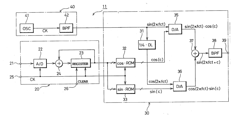
Figure 3 is the block diagram showing the
arrangement of the FM modulator according to the first
embodiment of the present invention. In the drawing, an FM
modulator 11 of Figure 3 comprises an integration circuit
20, a phase modulating circuit 30 and a carrier signal
generating circuit 40. Integration circuit 20 integrates
the analog modulation signal supplied to an input terminal
21. For example, a video signal can be used as an analog
modulation signal. Phase modulating circuit 30 phase-
modulates the integration output of integration circuit 20
in response to the carrier signal applied from carrier
signal generating circuit 40.
FM modulator 11 of Figure 3 is structured to
digitally process the analog modulation signal supplied to
input terminal 21. Thus, integration circuit 20 has an A/D
converter 22 which converts the analog modulation signal (a
video signal of a still picture in the present embodiment)
supplied to input terminal 21 to a digital signal having a
predetermined number of bits (8 bits in the present
embodiment). The digitalized video signal is added in an
adder 24 to a video signal one clock cycle before being
outputted from a register 23. Adder 24 comprises 2n (n is
a positive integer) bits. In the present embodiment, it is
assumed that n = 5. Therefore, the least significant 8 bits
of adder 24 receive the 8-bit video signal as input, and the
remaining 2 bits receive no input. Then, the output
(comprising 10 bits) of adder 24 is again supplied to
register 23.
As in the foregoing, by sequentially adding video
signals one block before register 23, an integrated digital
video signal is obtained from register 23.
Employed as the clock signal CK for use in A/D
converter 22 and register 23 is an output from a reference
2030794
oscillator 41 included in carrier signal generating circuit
40. Reference oscillator 41 comprises a crystal oscillator
or the like. In the present embodiment in which a still-
picture video signal having a time base extended by a factor
of 15 is FM-modulated, 2.5MHz is used as a clock frequency
fc of reference oscillator 41. The clock signal CK is
supplied from an input terminal 25.
A clear signal is supplied to an input terminal 26
provided for register 23. The clear signal initializes the
contents of register 23. This takes into consideration also
that a video signal having a lost direct component is
supplied to input terminal 21. That is, even if the
supplied video signal includes no direct current component,
an initial value of register 23 is fixed by resetting the
contents of register 23 for each horizontal cycle at a tip
portion of a horizontal synchronizing signal. Therefore, an
integration value can be fixed at a level of the tip of the
synchronizing signal.
The video signal digitally integrated in
integration circuit 20 is supplied to phase modulating
circuit 30. Phase modulating circuit 30 is provided with
first and second waveform-converting ROMs 32 and 33. The
first and the second waveform converting ROMs 32 and 33
convert the input digital video signals (integration output)
to two digital video signals having phases orthogonal to
each other. That is, first and second waveform-converting
ROMs 32 and 33 store an amplitude value (digital signal)
corresponding to a cosine wave and an amplitude value
(digital signal) corresponding to a sine wave as shown in
Figure 2, respectively. In first and second waveform-
converting ROMs 32 and 33, amplitude values corresponding to
the level of the input digital video signal are
simultaneously accessed to output two digital video signals
having phases orthogonal to each other, that is, a cosine
digital video signal cos(c) and a sine digital video signal
sin(c). Herein, the above-described phase c corresponds to
c~
~, .
`~ -
7 2030794
the level of the input digital video signal (the level of
the integration output). The cosine digital video signal
cos(c) and the sine digital video signal sin(c) are used as
modulation signals, as will be described later.
The cosine digital video signal cos(c) is supplied
to a first D/A converter 35 comprising 2n bits. The sine
digital video signal sin(c) is supplied to a second D/A
converter 36 comprising 2n bits. First and second D/A
converters 35 and 36 receive analog carrier signals from
carrier signal generating circuit 40 in addition to the
digital video signals.
In carrier signal generating circuit 40, the
reference clock signal CK from reference oscillator 41 is
supplied to a band pass filter 42 wherein the signal is
converted to a sine wave signal sin(2~fct) having the same
frequency as that of the reference clock signal CK. Herein,
is a ratio of the circumference of a circle to its
diameter and t is a time (the same hereinafter).
The sine wave signal sin(2~fct) is supplied to a
1/4-cycle delay circuit 31, wherein the signal is delayed by
1/4 cycle. As a result, the sine wave signal sin(2~fct) is
converted to a cosine wave signal cos(2~fct). By using such
a 1/4-cycle delay circuit 31, the sine wave signal
sin(2~fct) can be converted to first and second carrier
signals having phases orthogonal to each other. Herein, the
first carrier signal is a sine carrier signal sin(2~fct) and
the second carrier signal is a cosine carrier signal
cos(2~fct).
The sine carrier signal sin(2~fct) and the cosine
digital video signal cos(c) are supplied to first D/A
converter 35. The cosine carrier signal cos(2~fct) and the
sine digital video signal sin(c) are supplied to second D/A
converter 36. First and second D/A converters 35 and 36 are
D/A converters having four quadrant multiplication function.
In other words, first and second D/A converters 35 and 36
are structured to have output amplitudes controlled by an
8 2030794
input carrier signal when an input digital video signal is
converted to an analog signal. For example, the DAC-7533,
a product of DATEL Corporation is used for such D/A
converters 35 and 36.
Therefore, first D/A converter 35 outputs an
analog signal as expressed by the following equation:
sin(2~fct) cos(c) ..- (1)
Second D/A converter 36 outputs an analog signal
as expressed by the following equation:
cos(2~fct) sin(c) ................. (2)
The output of first D/A converter 35 and the
output of second D/A converter 36 are applied to an analog
adder 37, wherein they are added. The output of analog
adder 37 is expressed by the following equation:
[sin(2~fct) cos(c)] + [cos(2~fct) sin(c)]
= sin(2~fct + c) ... (3)
As shown in the foregoing, analog adder 37 outputs
a sine carrier signal sin(2~fct+c) with a phase lead of c
over the sine carrier signal sin(2~fct). The sine carrier
signal sin(2~fct+c) is band-limited by a band pass filter
38, and is then output from an output terminal 39.
The sine carrier signal sin(2~fct+c) thus obtained
at output terminal 39 is a signal whose phase changes at a
high speed (1/fc = 400 nsec) for every cycle of a carrier
signal in response to an amplitude of an input video signal
for the carrier signal. This consequently means that FM
modulation is carried out.
Phase resolutions of the above-described sine
carrier signal sin(2~fct) and cosine carrier signal
cos(2~fct), input to first and second D/A converters 35 and
36, depend on the bit arrangements of first and second D/A
converters 35 and 36. For example, assuming that the first
and second D/A converters 35 and 36 each comprise 10 bits,
the phase resolution is 0.35 (= 360 . 1023).
' ;~
-
9 2030794
The relation between a minimum phase change dc and
a frequency change df per unit time is expressed by the
following equation:
df = (1/2~) (dc/dt) -- (4)
The relation between a minimum phase change dc and a maximum
frequency deviation ~f is accordingly expressed by the
following equation:
~ f = df (28-l) ... (5)
Thus, when
dc = 6.14 x 10⁻³ rad ................ (6)
dt = 400nsec (= 1/(fc = 2.5MHz)) ... (7)
it can be shown as follows:
~f = 0.623MHz ... (8)
df = 2443Hz ... (9)
wherein a completely linear relation is established between
the input voltage and the output frequency. That is, a
linear characteristic is obtained.
In the embodiment shown in Figure 3, it is assumed
that the carrier frequency fc is set to 2.5MHz which is a
level of a tip of a synchronization signal of a video
signal. In addition, the maximum frequency deviation ~f is
set to 0.623MHz, and frequency is modulated to be higher.
As described above, in the embodiment of Figure 3,
FM modulation is carried out through a digital processing of
a carrier signal operating for every cycle. As a result, it
is possible to achieve an FM modulator having a more
excellent linear characteristic and temperature
characteristic than those of a conventional analog system FM
modulator and having no higher distortion.
Figure 5 is the block diagram showing the
arrangement of the second embodiment of the present
invention. An FM modulator 12 shown in Figure 5 has the
same arrangement as that of the FM modulator 11 shown in
Figure 3, except for the following points. Since the same
reference numerals are allotted to corresponding parts, no
description of those parts will be made. FM modulator 12
lO 2030794
shown in Figure 5 is provided with a phase modulating
circuit 50 having a different arrangement from that of phase
modulating circuit 30 in FM modulator 11 of Figure 3. Phase
modulating circuit 50 comprises four D/A converters 35a,
35b, 36a and 36b. Each of the D/A converters 35a, 35b, 36a
and 36b comprises 5 bits and has a four quadrant
multiplication function. The most significant 5 bits out of
the 10 bits of the cosine digital video signal cos(c) are
supplied to D/A converter 35a, and the least significant 5
bits are supplied to D/A converter 35b. The most
significant 5 bits out of the 10 bits of the sine digital
video signal sin (c) are supplied to D/A converter 36a, and
the least significant 5 bits are supplied to D/A converter
36b. The cosine carrier signal sin(2~fct) is supplied to
D/A converter 35a, and the cosine carrier signal cos(2~fct)
is supplied to D/A converter 36a. The sine carrier signal
sin(2~fct), after having its level attenuated by 1/(2n-1) by
an attenuator 51, is supplied to D/A converter 35b. The
cosine carrier signal cos(2~fct), after having its level
attenuated to 1/(2n-1) by an attenuator 52, is supplied to
D/A converter 36b. Each output of D/A converters 35a, 35b,
36a and 36b is supplied to an analog adder 37, wherein an
addition of the same is carried out. The arrangements of
other parts in phase modulating circuit 50 are the same as
those of phase modulating circuit 30 in Figure 3.
When a maximum amplitude of a carrier signal is
resolved by n bits, that is, by 5 bits, a minimum resolution
width corresponds to 1/(25-1) of the maximum amplitude of the
carrier signal. Thus, it results in the minimum resolution
width of D/A converter 35a being further resolved by 5 bits
by means of attenuator 51 and D/A converter 35b. As a
result, the pair of D/A converters 35a and 35b and
attenuator 51 as a whole function as a D/A converter of 2n
bits. Similarly, the pair of D/A converters 36a and 36b and
attenuator 52 as a whole function as a D/A converter of 2n
bits.
~ 11 2030794
The foregoing embodiment shown in Figure 5
employing the 5-bit D/A converters can be manufactured at an
extremely reduced cost when compared with the embodiment
shown in Figure 3 employing the D/A converters comprising 10
bits.
The present invention is not limited to the above-
described embodiments shown in Figures 3 and 5. For
example, a sine wave signal and a cosine wave signal are
exchangeable in the above-described embodiments of Figures
3 and 5. They have completely the same effect because the
sine wave signal and the cosine wave signal are entirely the
same signals except that they are out of phase by 1/4 cycle.
Multiplication can be performed between sine waves or cosine
waves in D/A converters 35, 36, 35a, 35b, 36a and 36b.
Furthermore, analog adder 37 can perform a subtraction in
place of an addition.
Since D/A converters 35, 36, 35a, 35b, 36a and 36b
in the embodiments of Figures 3 and 5 require a processing
of digital video signals based on analog carrier signals of
a sine wave or a cosine wave, they cannot be comprised of
only simple logic circuits for logic operations of digital
signals. This makes circuit arrangements complicated.
A further embodiment of the present invention will
next be described with reference to the drawings. In this
embodiment improvements address the foregoing problems.
Figure 6 is the block diagram showing the
arrangement of the third embodiment of the present
invention. An FM modulator 13 of Figure 6 comprises an
integration circuit 20, a phase modulating circuit 60, and
a carrier signal generating circuit 70. The arrangement of
integration circuit 20 is the same as that of integration
circuit 20 in the embodiments of Figures 3 and 5. A video
signal digitally integrated in integration circuit 20 is
supplied to phase modulating circuit 60. Phase modulating
circuit 60 is provided with first and second waveform-
converting ROMs 32 and 33 having the same arrangements of
2030794
12
the embodiments shown in Figures 3 and 5. First waveform-
converting ROM 32 converts the output of integration circuit
20 to a cosine digital video signal cos(c), and second
waveform-converting ROM 33 converts the output of
integration circuit 20 to a sine digital video signal
sin(c). The phase (c) corresponds to the level of the input
digital video signal (the output of integration circuit 20).
The above-described cosine digital video signal
cos(c) and the sine digital video signal sin(c) are supplied
to first and second digital multipliers 61 and 62, each
comprising 2n bits. First and second digital multipliers 61
and 62 receive a supply of a digital carrier signal group CK
(CK0-CK3) from carrier signal generating circuit 70 in
addition to digital video signals.
Carrier signal generating circuit 70 includes a
reference oscillator 71 and a multi-stage frequency divider
72. Reference oscillator 71 comprises a crystal oscillator,
for example, and an oscillating frequency thereof is
selected to have a frequency four times those of reference
oscillators 41 in the embodiments of Figures 3 and 5, that
is, set to 2.5 x 4 = 10.OMHz. Multi-stage frequency divider
72 converts the reference clock signal 4CK from reference
oscillator 71 (see Figure 7(a)) to four digital carrier
signals CK0-CK3 (see Figures 7(b)-(e)) each out of phase by
~/2 to one another. Each of the digital carrier signals
CK0-CK3 has one-fourth the frequency of the reference clock
signal 4CK. Multi-stage frequency divider 72 comprises four
frequency dividers, each frequency-dividing the reference
clock signal 4CK by 1/4.
Assuming now that the digital carrier signal CK0
has a reference phase, the digital carrier signals CK1, CK2
and CK3 are out of phase by ~/2, 2~/2 and 3~/2 from the
digital carrier signal CK0, respectively. Assuming that the
digital carrier signal CK0 at a H (logical high) level is
defined as the state 1, the digital carrier signal CK1 at a
H level is defined as the state 0, the digital carrier
~'
2030794
13
signal CK2 at a H level is defined as the state -1 and the
digital carrier signal CK3 at a H level is defined as the
state 0, the analog signal having an amplitude repeatedly
changing in the order of state O~state l~state O~state -1
can be expressed by these digital carrier signals CK0-CK3.
The analog signal is a carrier signal obtained by
analogizing a digital carrier signal. That is, the above-
described respective states correspond to the amplitude
values of the sine wave signal sin(2~fct) having the same
frequency as that of the carrier signal CK0 at phases O,
~/2, 2~/2 and 3~/2, respectively. One sine wave signal
sin(2~fct) can be therefore expressed by the four digital
carrier signals CKO-CK3. In the following description, the
four digital carrier signals CK0-CK3 are referred to as sine
digital carrier signals sin(2~fct).
The digital carrier signal CK0 having a reference
phase is used as a clock signal for use in an A/D converter
22, a register 23 and first and second waveform-converting
ROMs 32 and 33. The digital carrier signal CKO is supplied
through an input terminal 25.
The four digital carrier signals CK0-CK3 forming
the sine digital carrier signal sin(2~fct) are supplied to
a one-clock delay circuit 63 comprising a register, for
example. In one-clock delay circuit 63, each of the four
digital carrier signals CK0-CK3 is delayed by one clock (1/4
cycle). The delay amount corresponds to ~/2 in phase, so
that one-clock delay circuit 63 outputs a cosine digital
carrier signal CKc {= cos(2~fct)}. That is with one-clock
delay circuit 63 provided, the digital carrier signal group
CK is converted to a first digital carrier signal group
{sine digital carrier signal sin(2~fct)} and a second
digital carrier signal group {cosine digital carrier signal
cos(2~fct)} having phases which are orthogonal to each
other.
The sine digital carrier signal sin(2~fct) and the
cosine digital video signal cos(c) are supplied to first
.
2030794
14
digital multiplier 61, and the cosine digital carrier signal
cos(2~fct) and the sine digital video signal sin(c) are
supplied to second digital multiplier 62.
A multiplication of first digital multiplier 61
will be described. For a four-quadrant multiplication using
the four digital carrier signals CK0-CK3 as sine digital
carrier signals, the following logic operation is carried
out by using the most significant bit signal D9 of the
cosine digital video signal cos(c) as a sign bit signal.
10state input output
o positive or negative output positive at
any time
1 positive or negative output the input
without conversion
-1 positive output the negative
inversion of the input
-1 negative input the positive
inversion of the output
Such a multiplication can be performed by a simple logic
circuit.
Figure 8 is a logic circuit diagram showing one
example of the arrangement of first digital multiplier 61
shown in Figure 6. It is pointed out that second digital
multiplier 62 has the same arrangement as that of Figure 8.
In Figure 8, first digital multiplier 61 comprising 10 bits
includes ten NAND gates 100-109 and ten exclusive OR gates
110-119. Bit signals D0-D9 forming the multiplication
digital video signal cos(c) having 10 bits are applied to
the corresponding NAND gates 100-109, respectively. The
digital carrier signals CK0 and CK2 are applied in common to
NAND gates 100-109. The outputs of NAND gates 100-10g are
applied to the corresponding exclusive OR gates 110-119,
respectively. The digital carrier signal CK3 is applied in
common to the exclusive OR gates 110-118 except the
exclusive OR gate 119 corresponding to the most significant
bit signal. The most significant bit signal D9 is a sign
~'
2030794
bit signal, and the corresponding exclusive OR gate 119
receives an inversion signal of the digital carrier signal
CK1.
Figures 9A and 9B show a logic relation between
S the input and the output of such first digital multiplier 61
as shown in Figure 8. Figure 9A shows a logic relation
between the input bit signals D0-D8 and the output bit
signals D0'-D8'. The upper columns of Figure 9A show the
logic of the output bit signal Di' when the input bit signal
Di (i = 0 - 8) is at a low level (this level is assumed to
be a logic O). The lower columns of Figure 9A show the
logic of the output bit signal Di' when the input bit signal
Di is at a H level (this level is assumed to be a logic 1).
As indicated in Figure 9A, the output bit signal Di' attains
a L level in the state O irrespective of the logic of the
input bit signal Di. In the state 1, the input is output
without conversion. In the state -1, the input is inverted
to be output.
Figure 9B shows the logic relation between the
input bit signal D9 and the output bit signal D9'. In
Figure 9B, it is assumed that "L" denotes (-) and "H"
denotes (+).
Next it is assumed that a zero point of an analog
carrier signal (sine wave signal) is denoted as "O (=
1000000000)", a minimum value thereof is denoted as "-512 (=
0000000000)" and a maximum value is "+511 (= 1111111111)".
In this case, the multiplication output at the state 0 is
zero, so that (1000000000) instead of (0000000000) should be
output. That is, the output bit signal D9' should attain a
H level. First digital multiplier 61 has logic allowing the
above. As is clear from Figure 9B, in the state 1 the input
bit signal D9 is output without conversion, and in the state
-1 the output is the inversion of the input bit signal D9.
As described previously, second digital multiplier
65 also has the same arrangement as that of first digital
,~
16 2030794
multiplier 61 and therefore no description will be made
thereof.
As described earlier, first and second digital
multipliers 61 and 62 can be constituted by simple logic
circuits only. First and second digital multipliers 61 and
62 attain digital multiplication outputs of a sine signal
and a cosine signal, respectively.
First digital multiplier 61 therefore outputs the
digital signal expressed by the following equation:
sin(2~fct) cos(c) ................. (11)
Second digital multiplier 62 outputs the digital
signal expressed by the following equation:
cos(2~fct) sin(c) ...(12)
The outputs of first and second digital
multipliers 61 and 62 are applied to a digital adder 66
through buffer registers 64 and 65, respectively. Digital
adder 66 outputs the digital signal expressed by the
following equation (13) by adding the output of first
digital multiplier 61 and the output of second digital
multiplier 62:
[sin(2~fct) cos(c)] + [cos(2~fct) sin(c)]
= sin(2~fct+c) ... (13)
As described above, digital adder 66 outputs a
sine digital carrier signal sin(2~fct+c) with a phase lag of
c with respect to the sine digital carrier signal
sin(2~fct). The sine digital carrier signal sin(2~fct+c) is
converted to an analog signal by a D/A converter 67. The
output of D/A converter 67 is band-limited by a band pass
filter 68, which is output through an output terminal 69.
The sine carrier signal sin(2~fct+c) thus obtained
at output terminal 69 is the same signal as the FM
modulation output obtained at output terminal 39 in Figures
3 and 5. Consequently, it results in the video signal input
to an input terminal 21 being FM modulated.
Figure 10 shows a band characteristic of band pass
filter 68. As shown in Figure 10, the band characteristic
2030 794
17
of band pass filter 41 is preferably selected such that the
attenuation amount is l/2n-1) or more at a frequency +4fo,
centered at the carrier frequency fo, and the frequency in
the range +l/2fo is allowed to pass satisfactorily.
In addition, a band pass filter 68 is preferably
selected such that its phase lag characteristic stays linear
in the frequency range of +(l/2fo), centered at the carrier
frequency fo, as shown in Figure 11.
The above-described phase resolutions of the sine
digital carrier signal sin(2~fct) and the cosine digital
carrier signal cos(2~fct) input to first and second digital
multipliers 61 and 62 depend on the bit arrangements and on
the first and second digital multipliers 61 and 62,
respectively. Assuming that each of the first and second
digital multipliers 61 and 62 comprises 10 bits, for
example, the phase resolution is 0.35 (= 360 . 1023). In
the embodiment of Figure 6, the relation between a minimum
2phase change dc and a frequency change df per unit time is
expressed by the following equation:
df = (1/2~) (dc/dt) ................. (14)
The relation between a minimum phase change dc and a maximum
frequency deviation ~f per unit time will be therefore
expressed by the following equation:
~f = df (28-l) ... (15)
Thus, when,
dc = 6.14 x 10⁻³ rad ... (16)
dt = 400nsec (=l/fc = 2.5MHz) ... (17)
it can be shown as follows,
~f = 0.623MHz ... (18)
df = 2443Hz .. 0 (19)
so that a completely linear relation is established between
the input voltage and the output frequency. That is, it has
a linear characteristic.
The embodiment of Figure 6 shows a case where the
carrier frequency fc is set to 2.5Mz, which corresponds to
a synchronization signal tip level of a video signal, and
~ 2030794
18
the maximum frequency deviation ~f is set to 0.623MHz so
that frequency is modulated to be higher.
Since a sine wave signal and a cosine wave signal
are completely the same signals except that they are out of
phase by 1/4 cycle, entirely the same effect can be obtained
if a sine wave signal and a cosine wave signal are exchanged
in the embodiment shown in Figure 6.
Digital multipliers 61 and 62 in the embodiment
shown in Figure 6 can be structured to multiply sine waves
by each other, or to multiply cosine waves by each other.
Furthermore, digital adder 66 can perform a
subtraction in place of an addition.
While in the embodiments shown in Figures 3, 5 and
6, first waveform-converting ROM 32 generates a cosine
digital video signal cos(c), and second waveform-converting
ROM 33 generates a sine digital video signal sin(c), it is
possible to generate sine and cosine digital video signals
by using either first or second waveform-converting ROM 32
or 33 because the sine digital video signal sin(c) and the
cosine digital video signal cos(c) have phases orthogonal to
each other.
As described in the foregoing, the FM modulator
according to the present invention is suitable for FM
modulating an analog signal such as a video signal.
~,