Note: Descriptions are shown in the official language in which they were submitted.
2 ~
The present invention relates to a composite circuit
board having a thick circuit conductor and thin circuit
conductor, and its manufacturing method.
A circuit board through which a relatively large
electrical current~ for example, one for driving a motor
flows requires a circuit conductor having a large cross~
sectional area. A conventional circuit board of this
type has a structure in which a punched-out circuit con-
ductor made by punching out a desirable circuit pattern
from a metal plate (copper, aluminum, etc) is integrally
fixed on an insulation substrate (see Published ~ -Unexamined Japanese Patent Application (PUJPA) No.
63-237495).
In such a circuit board, to fix a punched-out cir-
cuit conductor on an insulation substrate, a copper foil
pattern is formed on an insulation substrate, and a
punched-out circuit conductor is soldered thereon. -This is rather a complicated procedure. Further, the
punched-out circuit conductor, which is relatively
GO thick, inevitably creates a bump on the surface of the
insulation substrate for its thickness, causing great
irregularity on the circuit substrate surface and making
matter difficult for printing of a solder resist and
circuit conductor to be multi-layered.
The present invention has been achieved in consid- -
eration of the above problems, and the object thereof is
to provide a composite circuit board which is easy to ~ -
- ~o ,n~r~2~
- 2 - :
~-,'
manufacture, and ~uitable to be multi-layered. ;~
Another object of the invention i5 to provide a
composite circuit board in which the parts can be easily g
mounted.
According to an aspect of the present invention, there
is provided a composite circuit board comprising a ~ubstrate
compri~ing an insulating material, said substrate having a
first surface and a second surface; a thick circuit
conductor embedded in the substrate, said thick circuit -.~
conductor including a given portion thereof ~or electrically ~ .
connecting components to said thick circuit conductor, said
given portion being positioned at a predetermined position
within said substrate; said thick circuit conductor further
having a predetermined circuit pattern; a thin circuit
lS conductor having a predetermined pattern provided in at
least one of the first and second surfaces of said
substrate; said thin circuit conductor including a land
positioned on said substrate at a locating corresponding to -~
the predetermined position of the given portion of said
thick circuit conductor; conductor means for electrically
connecting said land of said thin circuit conductor and said :~ :
yiven portion of said thick circuit conductor; and said
thick circuit conductor having at least one aperture formed -:~
adjacent the given portion thereof for suppressing heat
diffusion.
According to another aspect of the present invention, ~:~
there is provided a method of manufacturing a composite :
circuit board, comprising the steps of providing an ~ :
insulating substrate having a first sur~ace and a second
surface; embeddin~ a thick. . . . . . . . . . . . . . . . ;~
. ~ , :~
: `. '~ ' . ~. - -
2 U 3 0 ~ 2 6
- 3
:'~
, ~ .
conductive plate into at least one of said first and second
surfaces of said substrate for forming a thick circuit conductor
in said substrate; the embedded thick conductive plate having a
predetermined circuit pattern in which preselected conductive
portions of said pattern are interconnected by a plurality of ¦~
bridge portions of said pattern, said predetermined circuit :~
pattern including a given portion for electrically connecting ~ :
components to the thick conductive plate, said given portion ;
being positioned at a preset position in said substrate; using
the thus formed substrate with the thick conductive plate .. ~ .
embedded therein and having said predetermined circuit pattern,
to form an internal circuit plate by removing at least some of
the plurality of bridge portions of said predetermined circuit .
pattern; positioning at least one prepreg sheet over at least one .
of the first and second surfaces of said substrate that has the
thick conductive plate embedded therein; providing a thin circuit
conductor over a top one of said at least one prepreg sheet;
integrating said internal circuit plate, said at least one
prepreg sheet, and said thin circuit conductor to form an
integrated circuit board; forming the thin circuit conductor
into a predetermined pattern including a:land portion formed at
a selected position on said substrate which corresponds to the
predetermined position on said substrate of the given portion of .
said thick conductive plate; forming a through hole in said
integrated circuit board adjacent said given portion of said
thick conductive plate, said through hole having an internal .`
. ~ ' :; '
: - .:,',. .. " ::
r ~ ,
2 IJ 3 0 ~ 2 t~
- 3a -
wall; and providing conductor means on said internal wall of said
through hole for electrically connecting sa:id given portion of
said thick conductive plate and said land portion of said thin
circuit conductor together.
This invention can be more fully understood from the
following detailed description when taken in conjunction with -
the accompanying drawings, in which: -
Fig. 1 is a diagonal view showing the main section of a
: ' ~ . ~ ' ,. . ;,
composite circuit board having a thick circuit board in its
surface area; ~ --
Fig. 2 is a view explaining a method of manufacturing the ~ ~
circuit board shown in Fig. l; -- `
Fig. 3 is a plane view of a circuit pattern of a thick ~-
circuit conductor which is prepared by punching-out method;
Fig. 4 is a diagonal view showing the main section of a
composite circuit board according to an embodiment of the present
invention;
Fig. 5 is a cross section of a conductor m~ans of the
circuit board shown in Fig. 4;
Fig. 6 is a view explaining a method of manufacturing the
circuit board shown in Fig. 4; and . . . . . . . . . . . . . .
1/ '~' '"'''.'.' ''
., ':~'. ` ,-'
`"- ` ``.,`"'. `''-
"- ' .. .
o ~
Fig. 7 is a plane view showing of another circuit ~ -
pattern of the thick circuit conductor which is prepared by
the punching-out method.
Prior to the present invention, the inventors of this
invention discov red a method of manufacturing a circuit
board of this type by a hot press method, to solve the i~
problems stated above.
Fig. 1 illustrates an embodiment of a composite circuit
substrate manufactured by the above method, the figure
showing a thick circuit conductor 11 for a large current
flow of, for example, a power circuit, thin circuit
conductor 12 for a small current flow such as o~ a signal ~-
circuit, and an insulation substrate 13, and through hole ~ -
14, the inner surface of which is plated. AS shown in this
figure, the composite circuit board has a structure in which
the thick circuit conductor 11 is embedded in the surface
area of the insulation substrate 13, and the thin cixcuit
conductor 12 is embedded in the insulation substrate 13.
To manufacture a circuit board of this type, the method ;
shown in Fig. 2 is employed,. In this method, first, an
internal circuit board 16 having the thin circuit conductor ;
12 formed by etching a pattern on the copper foil on both
(or either) sides (or side) on an insulation sheet 15 is
prepared. The appropriate number of prepreg sheets 17 and
the thick circuit conductor 11. . . O . . . . . . . . . . .
. ' `..: - . . '
- ~ . . - ., .
X ' ,''`` ~``'```
~ ~ 3 ~
_
¦ formed into a desired circuit pattern by the punching- -~
out method are laminated on both sides of the internal
circuit board 16, and heated and pressed by hot press
machine 18. Thus, the insulation sheet 15 and the
prepreg sheets 17 are integrated into the insulation
substrate 13 shown in Fig. l, in the surface area of~ -
which the thick circuit conductor ll is embedded. The
~' thickness of the thick circuit conductor is generally
about 0.1-lmm, and that of the thin circuit conductor 12
is generally 35-70 ~m.
~ The thick circuit conductor ll is punched out into ~-
I a pattern shown in Fig. 3. With this pattern, a prede-
termined circuit pattern can be maintained through the
punching-out process. More specifically, this thick
circuit pattern ls has an arrangement in which each of ---
the thick circuit conductor ll is formed into a prede- ~-
termined circuit pattern in a square frame edge 21, and
thick circuit conductors ll located next to each other -~ ~:
are connected by bridges 22, and so are thick circuit ~-
conductors ll and the frame edge 21. Each of the thick
circuit conductors 11 has a hole 23 for forming a ~-
through hole, and the edge frame 21 has holes ~4 for `~`-
locating the conductor 11. ~ ~-
The bridges 22 is removed by cutting them off or ~-~
punching them out after integrating them into the insu-
lation substrate 13 as in Fig. l. In this figure,
numerals 25 denotes the sections where the bridges 22
: "' ,`':; ~-'.
.~: . - .
: -:: . . .- - . ~,. -
have been removed.
However, due to such a structure in which the thick
circuit conductor is embedded in the surface area of the
composite circuit board, to mount a part, the lead wire
of the part is soldered to the thick circuit conductor.
Since the thick circuit conductor has a large heat
,~
capacity, the heat is likely to diffuse, making the sol~
dering work very difficult. Further, the sections where -~
the bridges have been removed remain in the form of hole
or recess, in which some foreign materials are likely to ~-
accumulate, deteriorating the insulating property of the
board.
Meanwhile, the composite circuit board of the pre~
sent invention comprises a substrate made of an insulat~
ing material, a thick circuit conductor, embedded in -
this substrate, which includes a parts-mounting section ~`-
and has a predetermined circuit pattern, a thin circuit
conductor, provided on the surface of said substrate,
which includes a land corresponding to the parts- -
- . - :. .:...~. ~
mounting section of said thick circuit conductor and has
a predetermined circuit pattern, and a conductor means -
.. -. i: i: . . i -.
for electrically connecting said land and said parts- --
mounting section. Due to this structure, the above- ~-
mentioned problems can be solved without extinguishing - -
advantages such as to be easily manufactured, and suita~
ble to be multi-layered.
In other words, such a circuit board can be `~
. . ~, . .
:` . ` ' ',' `~' '
- 7
manufactured by the hot press method as in the case of -~
the above composite circuit board. Therefore, it is ;--
easily manufactured and is suitable to be multi-layered. ~ ~
Further, when mounting parts, all that is required is to ;-- ;
put the lead wire of a part through the through hole and
solder it to the land of the thin circuit conductor,
.. ~V.,,:,i;"
where diffusion of heat is less. Therefore, soldering
can be performed easily and the parts can be accurately
mounted. Moreover, since the thick circuit conductor is
embedded in the insulation substrate, the section where
the bridge has been cut off does not appear on the sur-
face thereof, improving the reliability of the circuit
in terms of insulation. -
The embodiments of the present invention will be
described in detail.
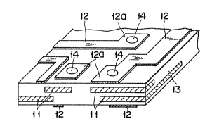
Fig. 4 is a diagonal view showing the main section
of a composite circuit board according to an embodiment
of the present invention, and Pig. 5 is a cross section ~-~
of a through hole forming portion thereof. -
In Fig. 4, members havlng the same functions as
those of Flg. 1 have the same reference numerals '~
thereof. ~
The composite circuit board shown in these figures
comprises an insulatlon substrate 13, a thick circuit ~ h-
conductor 11 embedded in the substrate and formed into a
predetermined circuit pattern, and a thin circuit con-
ductor 12 provided on the surface of said substrate and `~
~ .. ..... :
~ '.'
~Q~J~
- 8 -
formed into a predetermined circuit pattern. The thick
circuit conductor 11 includes part-mounting sections lla
on which the parts are mounted, and the thin circuit
conductor 12 has lands 12a at the posi.tions correspond-
ing to the part-mounting sections lla. This composite
circuit board has through holes 14 formed thereon so
that the parts-mounting sections lla and lands 12a are
conducted with each other. A conducting members 14a is
formed on the inner wall of each of the through holes 14
by plating. ;
In the case of such a structure, all that is
required in order to mount the parts on the thick cir-
cuit conductor 11 is to pass the lead wire of a part --
through a through hole 14, and solder it to a land 12a
of the thin circuit conductor 12. Some of the solder -
comes into the through hole 14. -~
Meanwhile, the thick circuit conductor 11 is the ` -~
same as that shown in Fig. 3, and can be formed into a
predetermined circuit pattern by, for example, the
punching-out method. Although the thick circuit conduc- `
tor 11 is embedded into the insulation substrate 13, if ~ -`
the thick circuit conductor 11 is formed as wide as
j possible, and the insulation layer between the thick and -
thin circuit conductors 11 and 12 is formed as thln as ;
possible, heat emission upon conducting electricity can
be suppressed, and the heat can be radiated.
Such a composite circuit board can be manufactured,
`
~ Q ~
g
for example, as shown in Fig. 6. F~rst, an internal
circuit plate 27 in which thick circuit conductors 11 ~ -
are embedded in both (or either) surface areas of the
insulation substrate 26, is formed. To manufacture ;
internal circuit plate 27, a thick circuit pattern, as
shown in Fig. 6, which is formed by punching out a cop~
per plate or by etching both surfaces is stacked on both
surfaces of a plurality of prepreg sheets prepared by ~-
laminating. Then, the circuit pattern is hot-pressed,
and the bridges are removed by punching out or cutting
off, thereby forming an internal circuit plate 27.
Next, the prepreg sheets 28 are stacked on both surface :
of the internal circuit plate 27, and a copper laminated ~-
plates 29 are stacked on the prepreg sheets 28 - ~ -
respectively, with a copper foil 31 facing outside.
These laminated layers are heated and pressed into an
integrated body by a hot press machine 18. During this
step, the holes or recesses formed at the sections where - - '
the bridge has been cut off are filled with resin flown
out of the prepreg sheets 28. After that, the surface
copper foil 31 is etched into a desired pattern to form
a thin circuit conductor 12 such as that shown in `-
Fig. 4. The conductor 12 thus formed is worked to make
holes, and the inner surface of each of the holes is - - `
plated, whereby through holes 14 are completed~
In this embodiment, a thin circuit conductor is
formed by etching copper foil into a desired pattern
., : ;.. :. - . ~. ............................................ - . - ,
; :~ . . . - : . :
- 1 0 -
(the subtractive method); however formation of the con-
ductor is not limited to this method. For example, the
additive method (in which a circuit pattern is formed on
the surface of an insulation substrate by using only
electroless plating or using both electrolytic and ~;
..:.: .
electroless platings) can be also employed.
The following is an explanation of another embodi- - -
ment of the present invention. ;~
This embodiment is exactly the same as the other
embodiment mentioned previously except for the thick
circuit conductor.
i The thick circuit conductor ll is formed of a metal
which has a high heat conductivity; therefore soldering
heat is likely to diffused to the circuit conductor when
lS mounting the parts. In order for prevention of this
heat diffusion, a hole 40 is formed near the part- i
mounting section of the thick circuit conductor ll. - `
This hole 40 suppresses diffusion of the heat of the - .`
part-mounting section of the circuit conductor ll to the
other sections of the conductor. ThuS, the temperature
of the soldering section of the part-mounting section -
can be maintained high, and therefore soldering of the ~ `
parts can be carried out more accurately.
. . : ,.::
, ~
- ,: . . ~