Note: Descriptions are shown in the official language in which they were submitted.
20309 1 q
- -
RANGE SWITCHING DEVICE
This invention relates to a range switching device which
is particularly applicable to the detection of signal levels
generated by such instruments as light-intensity meters and
other quick response instruments.
Conventional auto-ranging instruments will be described
hereinbelow in conjunction with the drawings.
The present invention improves on the problems of the
prior art and an objective is to produce a low cost device
with quick response time.
In accordance with one aspect of the invention there is
provided an auto-ranging device comprising: a measuring A/D
converter; a range-switching A/D converter having a faster
processing speed than that of said measuring A/D converter and
connected in parallel therewith; a range-switching amplifier
receptive of an input signal for applying an output signal to
the measuring A/D converter and the range-switching A/D
converter and controllable to variably amplify the input
signal to produce the output signal; and controlling means
receptive of an output from said range-switching A/D converter
to control the amplification by the range-switching amplifier
to ad~ust the magnitude of said output signal such that when
the magnitude of the output signal exceeds a scale range of
said range switching A/D converter, said amplification is
A ~
2 20309 1 9
lowered and when the magnitude of the output signal is less
than a scale range of said range switching A/D converter, said
amplification is increased, whereby the adjusted output signal
is measurable with a predetermined range of scale capabilities
of said measuring A/D converter.
According to the invented range-switching device, the
signal to the control microprocessor is generated by the
range-switching amplifier (hereinafter referred to as
switching amplifier) from the range-switching A/D converter
(hereinafter referred to as switching converter) which is a
faster processing device than the measuring A/D converter.
The microprocessor alters the amplification factor of the
switching amplifier so that the observed signal data will fit
in a proper scale range for the measuring converter.
The invented range-switching device achieves rapid
processing speed because the switching action is governed by
the signal from the switching amplifier from the fast acting
switching A/D converter, which is provided separately to the
usual measuring A/D converter.
Furthermore, the cost is kept lower because the device
utilizes a slower but lower cost integrating-type converter in
the measuring A/D converter.
Brief Description of the Drawings
Figure 1 is a block diagram of a first preferred
embodiment of this invention which utilizes a switching A/D
converter in a light intensity meter circuitry.
A
~ 2030~ 1 9
Figure 2 is a diagram to explain the response time
difference between the conventional and the invented A/D
converter used in the present invention.
Figure 3 is a block diagram of a light intensity meter
circuit using the conventional range-switching circuitry.
Conventional auto-ranging instruments are provided with
an internal range switching unit to enable automatic switching
of a measured s-ignal so that it can be accommodated within the
scale ranges provided on the analogue to digital conversion
unit ~hereinafter referred to as A/D converter).
Currently available devices employ different techniques
for auto-ranging; for example, a U.S. Patent No. 4,827,191
teaches a technique of measuring the peak values and entering
them into the control section of an A/D converter to select an
appropriate scale range of a measuring instrument. Another
U.S. Patent No. 3,813,609, discloses a technique of adjusting
the level of the measured signal based on the output power of
an A/D converter.
However, the technique according to Patent No. 4,827,191
is applicable to A/D converters equipped with range-switching
capabilities, but not to those without such capability. On
the other hand, Patent No. 3,813,609 teaches that the time
between the reception of a signal and its digital output is
primarily governed by the processing speed of A/D conversion.
Precision measurements require the use of an A/D converter
having a large number of bits, resulting in relatively slow
4 20309 1 9
response. In order to shorten the response time, converters
such as successive approximation or flash type is required,
both of which are relatively expensive, thus making the
instruments containing such devices more costly.
The operation of such an A/D conversion unit similar to
the one described in the above mentioned Patent No. 3,813,609
is described in the following.
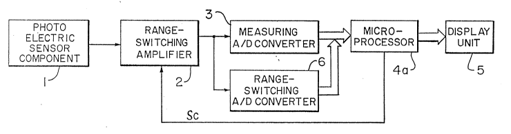
Figure 3 shows a schematic diagram of an instrument
having the A/D converter mentioned in the latter patent above.
In this instrument, photoelectric sensor component l, e.g.
photodiode, receives light energy and outputs it as electrical
energy. The range-switching amplifier 2 for the range-
switching unit receives a signal from said component 1 and
amplifies the signal according to a preset amplification
factor. The range-switching amplifier 2 is set to change the
amplification factor according to the magnitude of the
supplied signal Sc. The measuring A/D converter 3 converts the
signal from the range-switching amplifier 2 into a digital
form. The microprocessor 4 consists essentially of a CPU, a
ROM, a RAM and interface circuits (none of which is shown). A
control program for the CPU is stored in the ROM, which also
contains data regarding the input range of the measuring A/D
converter 3, i.e. the scale range limits.
Microprocessor 4 receives the signal from the A/D
converter 3, converts it into numerals and forwards the result
to a display unit 5. Microprocessor 4 also generates a
2030q 1 9
control signal to vary the amplification factor of the
range-switching amplifier 2 so that its output signal to
the A/D converter 3 will be within the input scale range.
The microprocessor 4 and the range-switching amplifier 2
constitute the range-switching circuitry.
When the magnitude of the output signal from the
amplifier 2 into the A/D converter exceeds the scale range of
such a light intensity measuring device, the excess signal
overflows from the converter. When the microprocessor 4
receives such an overflow indication, it generates a command
signal to decrement the amplification factor of the range-
switching amplifier 2. The amplifier 2 changes the
amplification factor accordingly by a certain amount. If the
microprocessor 4 still senses the overflow signal from the
amplifier 2, it outputs another command signal to lower the
amplification factor still further. This process is repeated
until the cessation of the overflow signal, from the amplifier
2 into the microprocessor 4, indicating that the magnitude of
the incoming signal is within the scale range of scale of the
A/D converter 3. At this time the microprocessor 4 accepts
the data from the converter 3, transforms the data into a
numerical form and displays the result on the display unit 5.
On the other hand, when a low level signal is received, the
microprocessor 4 continues to increase the amplification
factor until the signal magnitude reaches a measurable scale
range.
,~ .
6 203091q
As described above, the conventional meters operate by
following incremental trial processes of changing the
amplification factor of the range-switching amplifier 2 until
the data fit into one of the scale ranges of the measuring
device.
Such instruments have the following problems. First, the
response time of such circuits is necessarily long because the
whole process is predicated on successive trials of changing
the amplification factor until the results fit into a
permissible range. For example, if an integrating-type A/D
converter is used, the conversion times can range from several
milliseconds to several hundreds of milliseconds, making the
total response time well over one second for five trials. If
a faster successive approximation-type converter is used, the
conversion time could be shortened to several milliseconds.
However, such converters are relatively more expensive on the
basis of the number of bits.
Preferred embodiments of this invention are explained
below in reference to the figures mentioned above.
Figure 1 is a block diagram of a first preferred
embodiment of this invention which utilizes a switching
amplifier in a light intensity meter circuitry. The
invented circuitry, shown in Figure 1, differs from the
conventional circuitry, shown in Figure 3, in having a
range-switching A/D converter which outputs a signal
based on the data from a range-switching A/D converter 6,
20309 1 9
as well as the mi~u~locessor 4 to control the
amplification factor of the switch~ ng amplifier 2.
The switch~ ng converter 6 performs the conversion
process faster than the measuring converter 3. The
mi~lo~lu~essor 4a performs the same basic function as
previously mentioned mi~Lo~Locessor 4, that is to alter
the amplification factor of the switch~ ng amplifier 2 to
control the observed signal level to fit within a scale
range of a meter.
The above range-switch~ ng A/D converter 6 and the
microproc~.c~or 4a constitute the range-switch~ ng
circuitry.
According to this light intensity meter, the
observed analogue signal from the photoelectric component
1 is amplified by the switching amplifier 2, and the
amplified signal is forwarded to both measuring converter
3 and to a switch~ ng converter 6.
When the analogue signal rPAchec the swit~hi~g
converter 6, the signal is converted into a digital
signal, which is inputted into the microprocessor 4a.
The microprocessor 4a then compares the inputted signal
with the memory data in ROM, which define the upper and
the lower limits of stored values within a scale, then
determines the nene~ary value of amplification change
required for the switchi ng amplifier 2 . For example, if
a value PXCPP~ ~ ng the upper limit of the input level of
the measuring converter 3 is generated by the switch~ng
amplifier 2, then the mi~LG~locessor 4a output~ a command
signal to reduce the amplification factor in accor~ncP.
20309 1 9
with the output of the switrhi ng converter 6. The
switch~ ng amplifier reduces the output signal by the
corresponding amount. At this point, if the magnitude of
the signal re~rh~ng the measuring converter 3 still
~Ycee~ the level of said converter 3, then the above
process is repeated. That is, the microprocessor 4a
generates another signal to reduce the amplification
factor for the switch~ ng amplifier 2 by a predeterr~ n~A
amount in order to ~ te the observed signal within
a scale range. In this case, a switch~ng converter 6,
having a much higher processing speed than the measuring
converter 3, is used. Therefore, the output level of the
switrh~ng amplifier 2 n~e~ to fit within a scale range
of the measuring converter 3 can be deterr~ n~.~ quickly.
Furthermore, since the ,_ -n~ actions are
controlled by the dedicated switch ~ n~ converter 6, the
measuring converter 3 similarly can be dedicated to the
task of measuring. Therefore, the converter of choice in
a circuit of this type is a slower performing but
econo~ical integrating-type converter.
Figure 2 compares the performance times of the two
devices, conventional and the invented auto-ranging
devices; the ~onventional device is provided with a
measuring A/D converter 3 (a 12-bit integrating-type A/D
converter of 140 ms processing time) while the invented
device is provided with a switr,h ~ ng A/D converter (an 8-
bit successive approximation-type converter of 0.1 ms
processing time). As shown in this Figure, with four
2030~ 1 9 r- - -
range-switch1ng steps, the conventional range-switr,h~ ng
device requires;
140 ms X 5 ~ 700 ms
while the invented device requires
O.l ms X 4 + 140 ms ~ 140.4 ms.
It is clear that the measuring time is shorted by 559.6
ms by the use of the invented device.
In the above first preferred embodiment, a fast
acting switrh~ ng converter 6 was chosen but a second
preferred embodiment includes a switrh~ ng converter 6
having a lesser number of bits than that of the measuring
converter 3. It is also possible to use a comparator in
place of a switch1ng A/D converter 6.
S