Note: Descriptions are shown in the official language in which they were submitted.
20~0939
R09-89-044
MEMORY CARD RESIDENT DIAGNOSTIC TESTING
BACKGROUND OF TEIE INVENTION
The present invention relates to information
processing systems including multiple processing devices
linked to multiple memory cards of a main storage memory
through a shared interface, and more particularly to
means for executing processor initiated diagnostic
functions in the memory, while min;mi7;n~ traffic on the
interface .
In recent years, the performance of information
processing devices has improved considerably,
particularly in terms of more rapid processing of data.
Information processing networks increasingly employ
multiple processing devices sharing a common interface
for transmitting data between the processors and main
storage, which typically is composed of multiple memory
cards. The current trend is toward larger main storage
memories, employing greater numbers of such memory cards.
T, lU~. ~5 in memory subsystems have not kept pace with
improvements in processors. This is particularly evident
when multiple, parallel processors are used in the
network. Accordingly, system or network architectures
have been modified to compensate for main storage
memories which operate relatively slowly as compared to
the processing devices. Cache memories and other
techniques have been employed, in an attempt to uncouple
the processors from the memory cards in main storage.
Whenever a computer system is powered on, the system
is not immediately ready for use, but rather is subject
to final preparation known as initial program load ( IPL) .
This procedure involves installing initial programs into
the system, as well as final testing of the system,
including diagnostic testing of the memory arrays in main
storage. The arrays are composed of individual memory
locations or cells, each cell capable of storing a bit
representing either a logical one or a logical zero. The
2030939
R09-89-044 2
-
diagnosti~ testing is intended to confirm that the cells
are each capable of accurately storing logical ones and
logical zeros, and that no pair of cells are shorted
together .
In information processing networks utilizing
multiple processors, and multiple memory cards comprising
the main storage memory, the traditional approach to the
memory diagnostic test is to utilize one or more of the
processors to generate a predetermined data pattern and a
data stora command identifying a particular section of
the memory arrays, and to provide these to main storage
via the interface. The data pattern is written into the
selected section of the memory arrays, and is later read
back into the processor through a fetch command issued by
the processor. The fetched data is compared to the
original pattern to verify proper functioning of that
section of the memory arrays.
Of course, all of the memory arrays must be tested,
which consumes considerable time on the main storage
interface and requires substantial processor overhead.
In factj memory diagnostic tests typically consume from
ninety to ninety-five percent of IPL hardware test time.
While this problem arises in part from the number of
separate data patterns required to verify memory
integrity, the principle factor is the processor and
interace overhead involved in gaining access to the
memory. This difficulty increases with the number of
memory cards forming main storage, since a processor
performing the tests must access the memory cards
sequentially, without any overlap.
Among recent ~, L.~ s in memory testing
techniques are self testing memory devices. For example,
U.S. Patent No. 4,667,330 (Kumagai) discloses a self
diagnostic circuit formed on the same chip as the memory
arrays, for detecting defective cells. Data to be stored
into the arrays a~,so is provided to the self diagnostic
circuit, followed by a reading of the data out of the
2030939
F~09-89-044 3
arrays, and a comparison with data in the diagnostic
circuit. In U.S. Patent No. 4,757,503 (E~ayes et al) a
test generator, formed on a random access memory
integrated circuit, produces a predetermined test pattern
sequence applied to each of at least two storage arrays
in the RAM. Data in each column of one of the storage
arrays is compared with data in the eguivalent column of
the other storage array, with an error signal generated
in case of any disagreement.
U.S. Patent No. 4,782,486 (Lipcon et al) discloses a
self testing memory in which test patterns are written
simultaneously to all memory banks, by a central
processing unit through a commonly shared memory control
logic. Then, in connection with each memory board, the
contents of a reference memory bank is compared with the
contents of corresponding locations in the 1. -;nin~
memory banks.
While these approaches have proved satisfactory
under certain conditions, they fail to address the need
for rapid diagnostic testing of multiple memory cards in
a network in which such memory cards interact with
multiple processors through a shared interface.
Moreover, they reguire either comparison of different
arrays with one another, or logic on each chip, the cost
of which can be prohibitive for multiple-chip memory
c ards .
Therefore, it is an object of the present invention
to provide an information processing network in which a
processing device can, through a shared interface,
initiate overlapping or simultaneous diagnostic tests in
multiple memory cards.
Another ob~ect of the invention is to reduce the
time for manufactu~ing testing and initial program load
testing of memory arrays, by reducing the number of times
a processor (or a card tester) must gain access to the
arrays in the course of such testing.
2030939
RO9-89-044 4
-
Yet another object is to provide an information
processing network in which processor initiated
diagnostic testing of ~nemory arrays proceeds without
delay or interruption due to traffic on the memory
interface or asynchronous memory refresh operations
SUMMARY OF THE INVE:NTION
To achieve these and other objects, there is
provided a process fot diagnostic testing of memory
arrays, performed in a data processing system that
includes a configuratioll for mal~ipulating bit-encoded
data, a memory having memory arrays for storing
bit-encoded data, and all interface connected to the
processing config~lration and to the memory, for
transmitting the bit-el~coded data between the processing
device configuration and the memory. The process
includes the following steps:
using the processing configuration to generate a
compare command for storil~g bi.t-encoded data and address
informatiol~ correspol~di IICJ to ~ selected location in the
meloory arrays, and using the processing configuration to
generate a data pattern for s~lbsequent storage in the
selected location,
tral~smitting the compare command, address
information and data patterli to t~le memory via the
interface;
responsive to the command and address information,
storing the data pattern in a first register in the
memory, writing the data pattern into the arrays at the
selected location, reading data from the selected
location into a second register in the memory, and
comparing the data in the first alld second registers.
If the data in the first and second registers is the
same, the integrity of the arrays is verified.
2030939
R09-89-044 5
-
Differences between data in these registers causes the
identification of an error.
Preferably, the data processing system includes
multiple processing devices with the memory including
multiple memory cards, with the processing devices and
cards sharing a common main storage interface. At least
one of the processing devices includes logic for
generating "compare" commands and providing the compare
commands to the memory cards via the interface for
diagnostic testing of the memory cards, along with the
usual processor logic for providing store commands to
store data into the memory arrays, and fetch commands for
retrieving data from the arrays.
Each of the memory cards includes a hold register
for retaining a predetermined data pattern, supplied by
the proceGsing device along with the compare command,
Further, each memory card includes logic for writing the
data pattern into designated locations in the memory
arrays identified in the compare command. The data is
then read out of the arrays into a read back register on
the memory card, and the contents of the read back
register are compared to the contents of the hold
register. In the event of a disagreement, an error
message is provided to the processing device via the
interface.
As compared to the conventional approach of
diagnostic testing governed by the processing devices,
testing according to the present invention requires
substantially less time. Performing diagnostic testing
largely within main storage frees each processor to
perform other tasks during virtually all of the time
involved in memory array testing. Such other tasks can
include initiating further diagnostic tests in connection
with others of the multiple memory cards. rhe number of
cycles required to test each memory location or cell is
reduced, along with the time during which the interface
between the processors and memory cards is occupied.
2030939
R09-89-044 6
Once each of the memory cards receives a compare command
and accompanying data pattern, the card remains dedicated
to completing the diagnostic test function, without
interruption or other degradation from interface traffic
or asynchronous memory refresh operations.
IN THE DRAWINGS
For a further appreciation of the above and other
objects and advantages, reference is made to the
following detailed description and to the drawings, in
whi ch:
Figure 1 is a schematic view of an information
processing network in which multiple processing devices
are associated with a main storage memory including
multiple memory cards, through a shared interface;
Figure 2 is a timing diagram showing conventional
testing of memory arrays during the initial program load;
and
Figure 3 is a timing diagram similar to that in
Figure 2, showing memory array testing in accordance with
the present invention.
DETAILED DESCRIPTION OF THE ~h~hl~hla EMBODIMENT
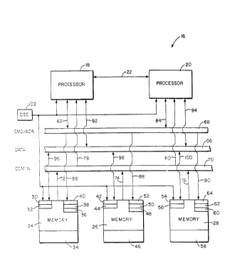
Turning now to the drawings, there is shown in
Figure 1 an information processing network 16 for storing
and performing selected operations upon bit-encoded data.
The system includes two processing devices, identified at
18 and 20, each with circuitry for performing operations
on data, and providing commands and related data for
transfer to and from main storage. An arbitration link
22 joins the two processors, and is used in combination
with arbitration logic residing in both processing
devices to assign priority to either processor in terms
of access to the interface. It is to be understood that
the configuration of processing devices in this network
R09-89-044 7 2030939
could consist of a single processing device, or multiple
processing devices in which m~lltiple arbitration links
are provided for a point-to-point connectioll o all
processing devices.
An interface connects the processing devices with
main storage, W}liCIl incl~ldes multiple memory cards such
as indicated at 24, 26 al~d 28. Memory card 24, for
example, includes a b~lffer 30, a l~old register 32, memory
arrays 34 for storing bit-ellcoded data, a compare
register 36, a status register 38 and logic circuitry 40
which includes a comparator circuit. ~ata stored in the
memory ar]-ays also is loaded into hold register 32 for
later comparison with dAta read out of the arrays and
into the compare register 36, using the comparator
circuit.
Memory card 26 is si.milar to memory card 24, and
includes a buffer 42, ~lold register 44, memory arrays 46,
a compare register 48, a stat~ls register 50, and logic
circuitry 52 incl~lding a comparator circuit. Likewise,
memory card 28 inc]udes a buffer S4, a hold register 56,
memory arrays 58, a compare register 60, a status
register 62 and logic circui try 64 . These compollents are
substantially identical to and function in the same
manner as their co~lnterparts in memory card 24. It is to
be understood that Inain storage can comprise Qny number
of memory cards S~IC}I as cardF. 24, 26 and 28.
The interface associatl.ng t~le processors and memory
cards includes a data b~ls 66, a command/address bus 68
and a communication b~ls 70, each joined to all of the
processing devices and memory cards, alld transmitting
data in parallel with t~le other buses. Lata bus 66
transmi.ts what can convelliently be called working
informati.on, i . e . information in which users of the
system have the most direct interest. Command/address
bus 68 transmits control information relating to commands
to fetch, store or otherwise manipulate particular
working data, and addr~ss information including a
i ~
R09-89-044 8 2030939
-
byte-aLigned start address at which data is currently
stored, or to which such data is to be stored, and the
address length in terms of the number of bits involved.
Communication bus 70 is used to transmit status
information from one of the memory cards to one of the
processing devices while sim~lltaneously transmitting
working information to tl~e processing device via the data
bus. Bus 70 also is used by a memory card to notify a
processing device that a memory card needs service, i.e.
is subject to internal error, trap condition, etc.
Communication lines 72, 74 and 76 enable the memory
cards to transmit stat~ls i.nformation to communication bus
70 and then to the ~ppropriate processing device via one
of the communication lines 78 and 80. Status information
is transmitted in only one direction, from one of the
memory cards to one of the processing devices.
Command lines 82 and 84 tra~lsmit command and address
information to b~ls 68, from w~lich one of command lines
86, 88 and 90 forwards information to the appropriate
memory card. Comlnand transfers are ~Inidirectional (from
processor to a memory card), the arrows at both ends of
command lines 82 and 84 indicating that eac~l processing
device, while transmitting a command, can inform the
remaining proces~ors as to the address and byte length of
the access.
Data lines 92 and 94 between processors and bus 66,
and dats lines 96, 98 and 100 between the memory cards
and the data bus, accommodate transmissions of working
information ill both directions. The interface includes
further data paths not illustrated in Figure 1, for
controlling use of data b~ls 66. For a further
explanation of the illterface, reference is made to U. S.
Patent No. 5,131,085, issued July 14, 1992, entitled
"High Performance Shared Main Storage Interface", filed
December 4, 1989, and assigned to the assignee of the
present application.
2030939
R09-89-044 9
A clock oscillator 102 provides a timing signal to
processing devices 18 and 20, and to memory cards 24, 26
and 28. The timing signal is comprised of individual
timing pulses generated at a predetermined timing
frequency, to provide uniform clock cycles.
When an information processing system is powered on,
the hardware is tested and certain initial programs are
loaded into the memory arrays, prior to any input from
the prospective user. This procedure, known as initial
program load ( IPL), includes the diagnostic testing of
memory arrays. To enhance user satisfaction, it is of
course desirable to complete the initial program load in
as short a time as possible, keeping in mind the need to
test the hardware, including the memory arrays,
sufficiently to verify their reliability. As previously
mentioned, diagnostic testing of the memory arrays
requires up to ninety-five percent of the time involved
in testing hardware. The current trend toward increased
main storage memory, whether through additional memory
cards, larger memory cards or both, underscores the need
for an improved approach to testing the memory arrays.
In accordance with the present invention, memory
array testing is accomplished more efficiently through
shifting of certain control logic from the processing
devices to the memory cards. The conventional,
processor-controlled approach to diagnostic testing is
illustrated in the timing diagram of Figure 2. A
processor issues a store command during the first cycle,
for transfer of a data pattern to a selected memory card
during clock cycle 2. The data pattern is a
predetermined series o~ logic ones and zeros, designed to
test memory array integrity. The selected memory card
begins to perform an access to its memory arrays in the
second clock cycle. More particularly, access to the
arrays is provided through two control lines, row address
strobe (RAS) and column address strobe (CAS). The row
address strobe initiates the data array access by going
active at the beginning of the second clock cycles, while
2030939
RO9-89-0~4 10
the column address strobe goes active at the beginning of
the fourth clock cycle. Once CAS i3 active, the data
pattern is written into the arrays at the selected
location. The row address and column address strobes
then go inactive.
In connection with Figures 2 and 3, it should be
noted that the RAS and CAS are shown going high as they
go active, aæ a matter of consistency with other lines.
In practice, RAS and CAS are "minus-active", i.e. going
active as the level goes low.
In cycle 7, the processor issues a fetch command.
The row address strobe and column address strobe go
active again, in cycles 8 and 9, respectively. Data is
read from the arrays during cycle 10, and transferred to
the processor during cycle 11. Fetched data is compared
with the original data during the twelfth clock cycle.
Figure 3 illustrates diagnostic testing of memory
arrays in accordance with the present invention. The
initial steps (through clock cycle 5), when performed on
one of memory cards 24, 26 and 28, are similar to the
steps of the conventional approach, the key difference
being that the processing device (e.g. processor 18)
issues a compare command rather than a store command. As
before, the data pattern is written to the memory arrays
(e.g. memory arrays on card 34) to a selected location,
during clock cycle 4. Further, however, the data pattern
is written to hold register 32 during cycle 4. The data
pattern is read back to the compare register 36 during
the eighth clock cycle. In the next cycle, the contents
of the compare register and hold register are compared in
logic circuitry 40. If the comparison yields no
differences in the contents of registers 32 and 36, the
integrity of the arrays, as to the data pattern and the
selected location, is verified. Conversely, responsive
to a difference at any of the bit positions, an error
condition is stored to status register 38, and an error
2030939
RO9-89-044 11
message is provided to processor 18 via communication bus
70 .
The timing diagram of Figure 3 is based on the
predetermined data pattern being written out to a single
location in the memory arrays. In fact, the logic
circuitry resident on each of the memory cards (at 40, 52
and ~4 respectively) can cause the data pattern to be
written simultaneously to multiple locations on multiple
chips on its associated memory card, a feature which
dramatically reduces the time necessary or memory array
te sti ng .
Thus, the circuitry resident on the memory cards
slightly increases the speed of testing the memory
arrays. Efficiency is increased beyond what this
comparison would suggest, however, since the above
examples assume that the processors in each case required
no time in contending for use of the interface. In any
configuration of multiple processors sharing a common
interface, in which multiple processors are employed in
memory array diagnostic testing, each processor involved
must contend with other processors for use of the main
storage interface. The conventional test sequence
(Figure 2) requires the processor to gain access to the
interface twice, once for storing the data pattern to the
memory card, and once for fetching data from the arrays.
Processor 18, by contrast, can test the arrays with only
one access to the main storage interface.
This gives rise to another advantage, in that the
diagnostic testing of memory arrays according to the
invention requires only half the amount of interface use,
specifically one cycle to provide the compare command,
while the conventional sequence requires two clock cycles
of interface usage. Once processing device 18, for
example, has issued a compare command to one of the
memory cards, the processor is freed for other activity
including the providing a compare command to one of the
other memory cards. Consequently, multiple memory array
2~30939
R09-89-044 12
-
tests of mlltiple memory cards can progress
simultaneously .
Yet another advantage arises from the fact that the
memory arrays are normally inactive, and require a
predetermined number of clock cycles to become charged or
ready for reading data from the memory arrays, or writing
data into them. The number of cycles needed of course
varies with the nature of the arrays and the cycle time,
but in any case adds to the time required for an access
to the arrays. The conventional test sequence requires
access to the memory arrays first to store data to the
memory arrays, and later, after the row address and
column address strobes have become inactive, to fetch the
data back from the arrays. By contrast, with the compare
function performed on the memory card, there is no need
to reactivate the row address strobe, which controls
activation of the memory arrays.
Another advantage, again in contrast to the
conventional sequence, is that asynchronous events such
as memory refresh do not interfere with diagnostic
testing of the memory cards. Such events can delay
conventional tests, particularly if they occur between
the store command and fetch command. Thus, an
information processing network in accordance with the
present invention, in which the memory cards of main
storsge test the memory arrays responsive to commands
from the processing devices, reduces the time and
interface usage required for tests.