Note: Descriptions are shown in the official language in which they were submitted.
2~3~
A CIRCUIT FOR SYNTHESIZING AN IMPEDANCE ACROSS THE TIP
AMD RING LEADS OF A TELEPHONE LINE CIRCUIT
CROSS REFERENCE TO RELATED APPLICATIONS
Cross Reference is made to the related Canadian
Patent Applications entitled: "A Solid State Telephone
Line Circuit," (Attorney Docket 89-1-032), nA High
Voltage 5ubscriber Line Interface Circuit,~ (Attorney
Docket 89~1-034), nA Tip-Ring Short Detector and Power
Shut-Down Circuit For A Telephone Line Circuit,~
(Attorney Docket 89-1-036), "A Thermal Protection Circuit
For An Integrated Circuit Subscriber Line Interface,~
(Attorney Docket 89-1-037), "A Thermal Protection
Arrangement For An Integrated Circuit Subscriber Line
Interface," (Attorney Docket 89-1-038), nA Control
Circuit For A Solid State Telephone Line Circuit,~
(Attorney Docket 89-1-0~9), and ~A Ring Trip Detector For
A Solid State Telephone Line Circuit," (Attorney Docket
89-1-040) filed on the same date, and by the same
assignee as this Application.
BACKGROUND OF THE INVENTION
1. Field of the Invention
The present invention relates to the field of
telecommunications and, more particularly, to a circuit
for synthesizing a floating complex impedance across the
tip and ring leads of a telephone line circuit.
2. Description of the Prior Art
Telephone line circuits are customarily found in the
telephone switching system or central office of a
telecommunications network. The telephone line circuit
interfaces the central office, to a telephone or
subscriber station found at a location remote from the
central office. The telephone line circuit functions to
supply power or battery feed to the subscriber station
via a two wire transmission line or subscriber loop and
:
,
'` ' ~' `
2~31~
to couple the intelligence or voice signal to and from
the telephone switching system.
In many presently known telephone line circuits the
battery feed function has hesn performed by using a
passive, highlv balanced, split winding transformer and
or inductors which carry up to 120ma dc. This passi~e
circuit has a wide dynamic range, passing noise-free
differential signals while not overloading with the 60Hz
longitudinal induced currents. The line circuit just
described, feeds dc current to the subscriber loop and
also provides the voice path for coupling the voice
signal between the subscriber station and the central
office. The electromagnetic components of passive line
circuits are normally bulky and heavy and consume large
amounts of power for short subscriber loop lengths were
the current fed to the subscriber station is more than
necessary for equalization. Active line-feed circuits
can be less bulky and require lower total power, but
meeting dynamic range and precision balance requirements
dictates an overly complex circuit design.
Recently, solid state replacements for the
electromagnetic components of the aforementioned line
circuits have been developed. Devices such as high
voltage bipolar transistors and other specialized
integrated circuits are being designed to replace the
heavy and bulky components of the electromagnetic line
circuit. Such a device is described in the IEEE JOURNAL
OF SOLID-STATE CIRCUITS VOL SC-16 NO. 4, August 1981,
,
entitled, nA High-Voltage IC for a Transformerless Trunk
30 and Subscriber Line Interface. n These smaller and
lighter components allow the manufacture of telephone
switching systems having more line circuits per circuit
card as well as decreasing the physical size of the
switching system.
However, presently known solid state line circuits,
still suffer from deficiencies in meeting good
transmission performance specifications. These
. .
.~ , : .
': ' , ,
~
203118 1
deficiencies manifest themselves in poor longitudinal
balance and poor longitudinal current susceptibility,
which cause the circuit to fail or to become noisy.
Other problems presently encountered are excessive power
dissipation at short loops that consume prodigious
amounts of central ofice power and 2 wire input
impedance circuits that are complex and that exhibit poor
return loss.
Accordingly, it is an object of the present
invention to provide a new and more effective circuit
that will effectively and efficiently synthesize a
complex floating impedance across the tip and ring leads
of a telephone line circuit matching the impedance of a
connected subscriber loop.
DISCLOSURE OF THE INVENTION
The above and other objects, advantages, and
capabilities are realized in a circuit which s~nthesizes
an input impedance and which is connected to a
subscribers loop via tip and ring leads. The circuit of
the present invention includes a tip drive amplifier
circuit connected to the tip lead of the subscriber loop.
The tip drive amplifier circuit is arranged to convert
feed voltage from a central office battery to tip feed
current on the subscriber loop. Similarly, a ring drive
amplifier circuit is connected to the ring lead of the
subscriber loop. The ring drive amplifier circuit is
arranged to convert feed voltage from a central office
battery to ring feed current on ths subscriber loop.
A common-mode amplifier circuit is included that is
connected between the tip and the ring leads of the
subscriber loop and to both the tip drive and the ring
drive amplifier circuits. The common-mode amplifier
circuit is arranged to sense the voltage dropped across
the subscrib~r loop and to output a control voltage to
tha tip drive and ring drive amplifier circuit. The
control voltage allows the tip drive and ring drive
~, . .
- -
.
. :: - . . , :
. . ~
--` 2~3~
amplifier circuits to offset the tip and ring feed
current applied to the subscriber loop, thereby,
developing a balanced longitudinal impedance to ground at
the tip and ring leads.
A differential amplifier circuit connected to the
tip and ring leads of the subscriber loop, is used to
detect a voltage difference between the tip lead and thP
ring lead. The differential amplifier circuit converts
the detected differential voltage into a single ended
10 output voltage of a specific gain.
The output voltage from the differential amplifier
circuit is coupled to a feedback circuit via a series
connected resistor and capacitor network.
The feedback circuit comprises an AC summing
15 amplifier circuit and a phase splitter amplifier circuit.
The AC summi~g amplifier circuit receives the
differential amplifier output voltage that is modified by
the values of the resistor and capacitor network. The AC
summing amplifier circuit develops and applies to the
20 phase splitter amplifier an impedance output signal.
The phase splitter amplifier circuit splits its
input signal into a pair of balanced output signals that
are equal in amplitude but 180 degrees out of phase with
each other. Eaah of the output signals are connected to
25 a respective one of the tip drive and ring drive
amplifier circuits where an input impedance equal to the
impedance of the subscriber loop is derived at the tip
leads and the ring leads.
BRIEF DESCRIPTION OF THE DRAWINGS
A better understanding of the invention may be had
from the consideration of the following detailed
description taken in conjunction with the accompanying
drawings in which:
Figure 1 is a block diagram of a solid state
35 telephone line circuit were the present invention is used
to advantage.
. .
. ~ , ~ ` :
.
. : . ::. : . . . . . , :
`~:' . . - ~ .
.' ' , " ` , :
2 ~ 8 ~
Figure 2 is a block diagram of the high voltage
subscriber line interface circuit.
Figure 3 is an electrical schematic showing the
impedance circuit, in accordance with the present
invention.
Figure 4 is an ac equivalent model of Figure 3, in
accordance with the present invention.
DESCRIPTXON OF A PREFERR~D EMBODIMENT
Directing attention first to Figure 1, a broad level
block diagram of a solid state telephone line circuit is
shown. The line circuit is shown driving a subscriber
station or telephone 10, via a subscriber loop 20. The
subscriber loop 20 is comprised of a twisted two wire
(2W) loop pair having a tip and a ring lead. The 2W loop
is connected from the subscriber station 10 to a High
Voltage Subscriber Line Interface Circuit (HVSLIC~ 30.
HVSLIC 30 feeds a -48 V dc voltage to the subscriber loop
across the tip and ring leads from a central office
battery (not shown). The HVSLIC 30 further functions to
superimpose a voice signal on the dc feed voltage and
also feed ringing current to subscriber loop 20 for
signalling. The HVSLIC 30 still further functions to
provide the 2W to 4W ~four wire) hybrid function of
splitting the balanced signal on the tip and ring leads
into separate transmit and receive paths that are ground
referenced.
The aontrol circuit 40 works in conjunction with the
HVSLIC 30 to provide the dc loop current shaping and the
line balance impedance portion of the 2W to 4W hybrid
function. The control circuit 40 further controls
various detection functions, such as, ring trip detection
and loop sense detection, as well as, providing a logic
interface to the central controller of the central office
switching system.
Most modern digital telephone switching systems use
Pulse Coded Modulation (PCM) digital data to convey voice
--5--
.,,,.. : ~. .. : : ; ::: : :: - . -
.: . , . ~ ., . . : .
:`: ' ' ' ';~ ' ' :~ ,. ~ ' -
, .~ : :: ,. . .
,: . : ~ .:
- , , : .
: . . . . , .. - , ~ ~ ,
'~' - : ,: .
2 0 ~
traffic through the central office switching system.
Therefore, some method of signal translation is required
to convert the analog voice signals received by the
interface circuit 30 to PCM digital data. This is
t~pically accomplished by a PCM codex and filter circuit
such as shown at 50. These devices are commercially
available as a so called CODEC/FILTER C~MB0~ from various
manufacturers. Such as the TP30XX family of COMB0
devices manufactured by the National Semiconductor
lo Company. Analog voice data from subscriber station 10 is
processed by the PCM codex 50 and applied to the PCM bus
of the central office switching system for transmission
to its destination. Similarly, the codex 50 re~eives PCM
data from the switching system and converts the PCM data
into analog signals which are superimposed on the dc feed
voltage of the subscriber loop 20.
The three solid state circuits 30, 40 and 50 just
described, in combination embody a complete solid state
line circuit adapted to ¢onnect a single subscriber
station to a central office switch.
Referring now to Figure 2, a broad level explanation
of the functions of HVSLIC 30, will now be given. The
HVSLIC 30 shown in Figure 2, is constructed as a bipolar
integrated circuit. All signals requiring high voltages
and currents are interfaced by this device. With the
addition of a few external discrete components a complete
transformerless line interface can be constructed.
The Tip Drive Amplifier circuit 31 and Ring Drive
Amplifier circuit 32 function to feed dc and ac voltages
and currents to the TIP and RING leads respectively of
subscriber loop 20. Voltage input into each amplifier 31
and 32 is converted into output current at the TIP lead
and RING lead respectively, of HVSLIC 30. The gain of
each amplifier circuits 31 and 32 is set by using four
precisely matched internal resistors and one precision
external resistor (not shown). Each amplifier circuit 31
. . . . .
,
: ` ' ' ' : . ; ' .
.
. , . : .
- ,.
.
-- 2~33 ~ 1
and 32 is capable of sourcing or sinking current
depending on the input voltage.
The tip and ring amplifier circuits 31, 32 are
connected to a Common-Mode Amplifier circuit 33.
Amplifier circuit 33 is used to sense the voltage across
the subscriber loop 20 and to amplify the voltage ~y a
factor of 3.33. The output of amplifier circuit 33 is
fed to amplifier circuit 31 and Amplifier circuit 32.
Amplifier circuit 33 is dc biased at one half of the
central office battery (~bat) or VB/2. The Common-Mode
Amplifier circuit 33 primarily functions to synthesize a
longitudinal (common-mode) input impedance at the TIP and
RING terminals of HVSLIC 30 that is a virtual ac ground.
Amplifier circuits 31, 32 and 33 are further
connected to a Tip-Ring Short Protection circuit 34.
Circuit 34 functions as a detector, which monitors the
output of the Common-Mode Amplifier circuit 33. If the
output of amplifier circuit 33 is 7.75 volts or closer to
either ground or Vbat, the detector places amplifier
circuits 31 and 32 into a high impedance mode. This
condition represents a combined short of the TIP and/or
RING leads to ground or Vbat. When in this short
condition, the Tip Drive Amplifier circuit 31 and Ring
Drive Amplifier circuit 32 are turned off to remove drive
current from the subscriber loop 20.
AC Sum Amplifier circuit 35 functions to sum the
receive voice signals with the transmit voice signals.
Amplifier circuit 35 provides a ground referenced summing
node at the SUMMA terminal of ~IVSLIC 30. The transmit
voice signals are fed to amplifier circuit 35 to
synthesize an input impedance of 900 ohms at 2.16~f at
the TIP and RING terminals, in accordance with the
present invention.
The AC Sum Amplifier circuit 35 is connected to
Phase Splitter Amplifier circuit 36. The Phase Splitter
Amplifier circuit 36 performs two functions. First, it
sums a dc control signal Erom the control circuit 40
,' ~ "' ~ ' ' '
. "' , .
.
.
~`, . .
2~3~
applied to terminal SUMB, with the summed receive and
transmit voice signals oukput by amplifier circuit 35.
Second, it level shifts and balances the now combined
signals abou~ VB/2 and applies the signals to two output
leads. The signals output from the each of tha two
output leads of amplifier circuit 36 are equal in
amplitude, but 180 degrees out of phase with each other.
One of the output leads of amplifier circuit 36 is
connected to the Tip Drive Amplifier circuit 31 and the
other to the Rin~ Drive Amplifier circuit 32.
The ~MT Differential amplifier 37 functions ~o
amplify the voltage difference between the TIP lead and
the RING lead of the subscribers loop 20 and applied to
terminals RPT and RPR, respectively. These voltage
differences which are analogous to the transmit voice
signals are amplified and converted into a single ended
output by amplifier circuit 37. The single ended voice
signals output from amplifier circuit 37 are connected to
terminal XMTA and applied via a coupling network (not
shown) to the SUMMA terminal. As explained earlier in
the description of the AC Sum Amplifier circuit 35, the
transmit voice signals applied to the SUM~IA terminal are
used by amplifier circuit 35 to synthesize the input
impedance at the TIP and RING terminals. The transmit
voice signals from XMTA are also applied to the control
circuit 40, to drive the transmit input of that circuit.
A scaled down representation of the signals output from
terminal XMT~ is output from terminal XMTB. The signals
from terminal XMTB are applied to a dc loop control
circuit (not shown) on control circuit 40.
A Tip Party Mark Detector circuit 38 is connected to
the common mode amplifier 33 and the VBAT/2 battery
reference circuit 39. Detector 38 functions to sense a
difference voltage between the output of Common-Mode
Amplifier circuit 33 and the VB/2 voltage generated by
circuit 39. When a difference is sensed a logic signal
is generated by detector 38 and applied to the TPM
- ;
- ~:
: . , . . ' . ' . ~ .
.;
. . . . . .
: :
`:
203118 ~
terminal. Under normal operating con~itions, the output
voltage of amplifier circuit 33 equals the VB/2 reference
voltage. However, when a tip party mark is placed on
line, the tip current will not equal the ring current.
When the voltage from amplifier circuit 33 is
sufficiently different than VB/2 the detector trips and
outputs its logic signals at terminal TPM.
The VBAT/2 circuit 39 generates from the central
office battery (not shown) a reference ~oltage which is
lo approximately one half of the central office batter~
voltage input at VBAT. The VB/~ output voltage of
circuit 39 is used as a reference by the Common-Mode 33,
Phase-Splitter 36 and XMT Differential 37 amplifiers, as
well as the Tip-Ring Short Protection circuit 34. A
scaled down voltage output is generated by circuit 39 and
output from the SVB terminal. This output is used by the
aforementioned dc loop control circuit of control circuit
40.
Finally, a Power Down and Thermal Shut Down circuit
131 is included which controls the power dissipation of
the HVSLIC 30. The power down function of circuit 131
includes logic input controls arranged to receive logic
input signals at terminal TRHZ. When the logic signal at
TRHZ is a logic high or "1", all internal HVSLIC 30
amplifiers are put into a high impedance mode. The
output drive current and internal bias current to all the
amplifiers of HVSLIC 30 is cut off, and thus, the power
consumption of HVSLIC 30 is reduced to a minimum. When a
logic low or "0" is applied to TRHZ khe HVSLIC 30 circuit
functions normally. The thermal shut-down function of
circuit 131 senses the temperature of HVSLIC 30 and cuts
off drive current and internal bias current to the HVSLIC
30 amplifiers if the temperature reaches above 100
degrees C. Therefore, trimming power dissipation.
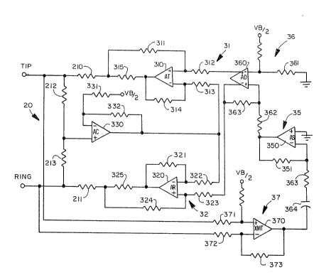
Turning now to Figure 3, the Tip Drive, Ring Drive,
Common-Mode, Phase-Splitter, AC Sum amplifier, and XMT
Differential amplifier circuits, are shown, and in
~.,~ . .
~ . ~
.
2 ~ 3 ~
combination provide tha floating point impedance of the
present invention.
There are only two methods of feeding a subscriber
loop while maintaining control of the dc and ac
impedances required by the circuit. The first method
uses voltage drive with series current feedback control.
The second, uses current drive with shunt voltage
feedback con~rol. The second feed method avoids
potential circuit instability which often occurs when a
voltage output opPrational amplifier has a heavy
capacitive load. The feed circuit of the present
invention uses this second method.
Figure 3, of the included drawings, shows a
subscriber loop termination comprising of a TIP lead and
a RING lead. Resistors 212 and 213 combine the TIP and
RING voltages and feed the common-mode signal to the
Common Mode Amplifier (AC) circuit 33. Tip Drive
Amplifier (AT) circuit 31 comprises operational amplifier
(op amp) 310, and resistors 311 through 315. Similarly,
a Ring Drive Amplifier (AR) circuit 32 comprises op amp
320 and resistors 321 through 325. Resistors 315 and 325
are the feed resistors (RF) of amplifier circuits 31 and
32 respectively. The two symmetrical amplifier circuits
31 and 32 are configured as transconductance amplifiers
having a voltage to current gain. AT Amplifier circuit
31 provides drive current to the TIP lead of subscriber
loop 20 and AR amplifier circuit 32 provides drive
current to the RING lead of the subscriber loop. The
transconductance amplifier circuit of each circuit 31, 32
has a differential input and a bi-directional output so
that current can be sourced or sunk depending on the
differential input voltage applied to the non-inverting
(positive) and inverting (negative) inputs of each op amp
310, 320.
A Common-mode Amplifier circuit (AC) 33 comprises op
amp 330 and resistors 331 and 332. AC Amplifier circuit
33 is used to drive the inverting (negative) inputs of op
--10--
' ' ~ ; -- ' ' : ' .
~-: - ; ' . , ;:
: . . ., :
. . . ~ .
~ 203~1 8~.
amps 310 and 320. ~esistors 21~ and 213 combine the TIP
and RING voltages and feed the common-mode signal to the
positive input of op Amp 330. The output of AC amplifier
circuit 33 is a function of the bias voltage VB/2,
developed by the VBAT/2 voltage reference circuit 39
shown on FigurP 2 and the common-mode voltage (Vcm). Vcm
can be expressed as:
VTIP + VRING
Vcm = ------~~~~~~
When the AC amplifier circuit 33 is connected to
amplifier circuits 31 and 32, for a given voltage
difference between the positive and negative inputs of op
amp 310 and 320 the voltage vcm will be equal to VB/2, or
one half the effective central office battery voltage.
The loop resistance of subscriber loop 20 floats between
the voltage at the TIP and RING leads. The negative
feedback produced by AC amplifier circuit 33 is such that
common voltages induced on the TIP and RING leads will
tend to offset in an equal malmer the drive at the
outputs of op amps 310, 320. This provides a balanced
longitudinal impedance to ground. When
(RP+RF)(gm)(l+Ra/Rb)=l the outputs of op amps 310 and 320
are at an ac virtual ground for any value of longitudinal
current. That is, the voltage output by op amps 310 and
320, will not fluctuate as longitudinal current varies.
Therefore, the longitudinal impedance can be simply
expressed as (RP+RF) at the TIP and RING leads. In
principle a large value of longitudinal current that is
within the current carrying capacities of amplifiers 31
and 32 can be handled by the amplifier circuits without `-
incidences of voltage excursions at their outputs.
The common-mode feedback developed by AC amplifier
circuit 33 only effects signals common to the TIP and
RIN~ leads of the subscriber loop 20 and has no effect on
the differential signals. One advantage to the
arrangement sho~n in figure 3, is that the common-mode
.: . . .
~:, . ; . - . .
- . .
.. ~ . .. . . :
2~3~8:1
feedbac~ i5 taken after resistors 210 and 211 or the RP
resistors. A close matching of RP, over a long period
can not be guaranteed due to lightning surges. However,
common-mode feedback taken a~ter the RP resistoræ allows
for circuit balance that is insensitive to RP matchingO
Differential signals transmitted on the TIP and RING
leads of the subscriber loop 20 are detected and
amplified by Differential Amplifier (XMT) circuit 37.
XMT amplifier circuit 37 includes an op amp 370 having
its positive lead connected to an input resistor 371 and
to the TIP lead. The negative lead of op amp 370 is
connected to input resistor 372 and the RING lead. The
single ended output of op amp 370 is also connected to
feedback resistor 373. Amplifier circuit 37 functions to
amplify the voltage difference between the TIP lead and
the RING lead of the subscribers loop 20. The single
ended signals output from op amp 370 are connected to
summing amplifier circuit 35 via capacitor 36~ and
resistor 363.
The single ended output signal from XMT amplifier
circuit 37 is next applied to AC Sum Amplifier (AS)
circuit 35 and Phase Splitter Amplifier (AD) circuit 36.
AD amplifiar circuit 36 includes op amp 360, input
resistors 361, 362 and feedback resistor 363. The
positive output of op amp 360 is connected via resistor
312 to the positive input of op amp 310 of the AT
amplifier circuit 31. The negative output of op amp 360
is connected to the positive input of op amp 320 of the
AR amplifier circuit 32. The output developed by op amp
360 is level shifted and referenced to VB/2. The
positive and negative output signals are balanced around
half the central office battery voltage. The signals
output from the two output leads of op amp 360 are equal
in amplitude, but 180 degrees out of phase with each
other.
The AS amplifier circuit 35 includes op amp 350 and
resistor 351. The negative input of op amp 350 is
.. . . . . .
` . . . ' . '; ' ' ' . ' ' -
.. .
,
.- ~ . - -
. . .
2~18~
connected to op amp 370 via capacitor 364 and resistor
363. The output of op amp 350 is connected to the
positive input of op amp 360.
AS amplifier circuit 35 functions to provide a
ground referenced summing node for signals output from
XMT Differential Amplifier circuit 37. The summation of
the signals synthesize a 900 ohm 2.16 f input impedance
across the TIP and RING leads. This value of impedance
is required to match the twisted pair telephone line
impedance normally found in the subscriber loop~ The
value of capacitor 364 and resistor 363 combined with the
gain of the amplifiers in the circuit synthesize the
needed valus of input impedance.
Turning now to Figure 4, an ac equivalent circuit of
the TIP side of the ¢ircuit of Figure 3 is shown. The
derivation of the input impedance can be expressed
mathematically by the following formulas:
v
(a) Zin = ------
in = Rin + --------
jwCin
(b) = Rin (1 + -------)
jwRinCin
i = v x loop gain x gm
R10
= v [(XMT) x AD x (---------) gm]
Rll -~ 1
__________
jwCl
v Rll
[ ~----------------] [ 1 + ]
i XMT x AD x gm x R10 jwRllCl
-13-
. . . .
` ~ .
;: , ' ` ~: ', ': ' ' ; '
. .
- 203~
Therefore, from formulas a, b and c, the input
resistance Rin and input capacitance Cin can be expressed
by the following circuit relationships.
1 Rll
Rin (1 ~ ) = [---~ -----------] [1 + ------]
jwRinCin XMT x AD x gm x R10 jwRllCl
Rll
X~T x AD x gm x R10
Rin Cin = Rll Cl
Rll Cl
Cin = ------- ;
Rin
Plugging values to the components of Figure 3, the
current gain or gm at amplifier AT can be found. For
example, if resistor 311 (Rc) has a value of 20K ohms,
resistors 312 (Ri) a value of lOOK ohms and resistor 210
(Rf) a value of 50 ohms, then the current gain of the AT
amplifier circuit can be expressed as:
Rc
gm = ---_____
Ri x Rf
gm = 4mA/V -~
The gain for amplifiers XMT and AD can be found in a
similar fashion. For amplifier XMT the gain is
calculated as 0.5 for resistor values of 44K ohms for
resistors 371 and 22k ohms for resistor 373. The gain
for amplifier AD is calculated as 1.0 for resistor values
of 108k ohms for resistor 362 and 363.
The impedance of the equivalent circuit can be
determined using the gains of the amplifiers just
calculated and inser~ing values for resistors R10 and Rll
and capacitor Cl. For example, given a value of llOK
-14-
. ~ . :. . . .
~03~
ohms for resistor Rlo, 200K ohms for resistor R11 and a
capacitance of 0.Ol~F for C1 and using the formulas
derived above for Rin and Cin, it can be shown that:
200K
Rin = ~
0.5 x 1 x 4mA/V x llOK
= 909 ohms ~ 900 ohms
200K x O.Ol~F
Cin = --- ---------------
O.909K
= 2.2~F
It will be appreciated by those skilled in the art
that a floating input impedance can be realized using the
feedback techniques taught by tha present invention. As
shown and explained above for a given value of
Capacitance (C1) and resistance (R11~ a complex impedance
can be realized across the TIP and RING leads of a
subscribers loop.
It will be obvious to those skilled in the art that
numerous modifications to the present invention can be
made without departing from the scope of the invention as
defined by the appended claims. In this context, it
should be recognized that the essence of the invention
resides in a new and more effective circuit that will
effectively and efficiently synthesize a complex floating
impedance across the tip and ring leads of a telephone
line circuit having the advantages and capabilities
described herein.
-15-
~ . . . .
~. . . .
. ~ . .
:. .