Note: Descriptions are shown in the official language in which they were submitted.
2031427
Pressure Sensor and Method of Manufacturing Same
The present invention relates to a pressure sensor as
set forth in claim 1 and to a method of manufacturing
same as set forth in cLaim 7. According to the wording
of claim 1, the pressure sensor has a substrate and a
diaphragm which are joined together, particularly in a
defined spaced relationship and para~Lel to each other,
forming a chamber sea(ed at least at the edge, wherein
- the substrate and/or the diaphragm are made of ceram-
ic, glass, or a single-crystal material,
- the side of the diaphragm facing the substrate ;c
covered with a layer of silicon carbide, niobium, or
tantalum which, in turn, is covered with a protective
layer and-serves as one capacitor electrode,
- the side of the substrate facins the diaphragm is
covered within the chamber with a-t least one addition-
al layer of any one of said materials which, in turn,
is covered with an additional protective layer and
serves as the second etc. capacitor electrode, and
- the substrate and the diaphragm are so~dered to-
gether by a formed part of active solder which also
serves as a spacer.
Investigations conducted by the inventors have shown that
conventional layer materials for capacitor e~ectrodes of
pressure sensors, such as copper, gold, silver, or platinum,
2031427
exhibit a number of disadvantageous effects which occur
during the active soldering of substrate and diaphragm,
which are coated with the electrodes. On the one hand,
the soLder, because of its good wetting -ability, spreads
over the electrode surface outside the joint, so that
the substrate and the diaphragm may be soldered together
in the electrode area. On the other hand, the electrode ma-
terial of the diaphragm, which material may be only 100 nm to
500 nm thick, for example, alloys so well with the solder
that interruptions of the electrical contact between sol-
der and electrode material may result.
Furthermore, conventional pure alumina ceramic and com-
mercially available active solders, containing 1 to 5%
titanium, differ widely in their thermal coefficients of
expansion, so that the zero-point and sensitivity tempera-
ture coefficients of the pressure sensor may be adversely
affected.
There is one application of pressure sensors, namely if
they are used as reference-pressure sensors, in which the
chamber communicates with the reference-pressure medium, e.g.,
the surrounding air. The moisture in the su,rounding air
gets into the chamber and, thus, to the capacitor elec-
trodes, where it may deposit under certain circumstances.
When a voltage from the circuit for measuring the pressure-
dependent capacitance change is applied, the electrodes
may thus corrode. Furthermore, contacting of the electrodes
by means of active-solder insets in the substrate requires
step soldering, i.e., at least two soldering steps.
2031427
Finally, the mechanical propert;es of the diaphragm must
not be impaired by too thick electrode layers, which is
why the above-mentioned thickness between 100 nm and
500 nm is required.
Accordingly, the object of the invention as claimed is
to avoid the problems described by an appropriate choice
of materials, i.e., to find for the capacitor electrodes,
their terminal pads, and the joints, in particular, suit-
able materials which do not have the disadvantages de-
scribed and do not place any undue constraints on the
selection of the process parameters. In addition, the
pressure sensor is to be usable at higher temperatures
than pressure sensors with glass-frit joints, and the
maximum load capacity of the diaphragm is to be determined
not by the strength of the joint, but only by the strength
of the diaphragm material. Finally, the manufacturing
costs are to be as low as possible.
It has been found that, if either of the high-melting-
point metals niobium and tantalum or silicon carbide is
used as electrode material, the "alloying away" of the
electrode material by the active solder can be practically
completely avoided over a wide soldering-temperature range.
A tantalum layer with a thickness of only 100 nm, for
example, easily withstands a 1000 C soldering process with
an active solder.
Spreading of the active solder over the electrodes and
corrosion of the latter are prevented by the protective
layers, which are oxides of the respective materials men-
tioned above. Thus, in the case of tantalum, this is pre-
ferably tantalum pentoxide. These oxide layers may be
2031427
4 28351-5
formed in a conventional manner by thermal or anodlc oxidatlon.
In the comblnatlon of all propertles, tantalum is the optlmum
electrode materlal. Although tantalum has a relatlvely hlgh
reslstlvity, pressure sensors wlth 100 nm thlck electrodes and a
capacltance of 50 pF have a Q of 3x10⁴ to 4x10⁴ at a test fre-
quency of 100 kHz.
Wlth the above-mentloned materials for the electrodes,
only a slngle solderlng operatlon ls necessary whereby both the
substrate and dlaphragm are iolned together and the electrodes are
contacted through a hlgh-vacuum-tlght seal. The latter ls prefer-
ably done from the slde of the substrate faclng away from the dla-
phragm by means of actlve-solder lnsets extendlng to the second
etc. capacltor electrode and the actlve solder, respectlvely, wlth
each capacltor electrode of the substrate havlng at the contact
polnt a caplllary stopper ln the form of a flare of the hole con-
talnlng the actlve-solder lnset.
The use of only thls slngle solderlng operation ls also
made possible by the ~ust mentloned capillary stopper, in whlch
the holes in the substrate may end on the chamber side. Thus, the
actlve solder, when becomlng llquld, cannot sklp the small gap
between the opposite capacltor electrodes due to capillary action,
which prevents it from advanclng to the plane of the electrode of
the substrate.
In accordance with the inventlon there is provlded a
method of manufacturlng a pressure sensor comprising a substrate
havlng passages in each of whlch ls flared at one end, and a dla-
phragm whlch forms a chamber wlth the substrate, comprlsing the
steps of:
,,
2031427
- depositing the capacitor electrodes on the dia-
phragm and the substrate,
- forming the protective layers on the capacitor
electrodes,
- introducing the active-solder insets into t-he holes
in the substrate,
- heating the coated and loaded substrate, the coated
diaphragm, and the interposed formed part of active
solder, preferably in a vacuum, until the active
solder has melted through, and
- allowing this assembly to cool down.
Further features and advantages of the ;nvention will be-
come apparent from the following description of embodi-
ments illustrated in the figures of the accompanying
drawings, where like parts are designated by like refer-
ence characters. In the drawings,
Fig. 1 is a top view of a first embodiment of a
pressure sensor in accordance with the invention;
Fig. 2 is a section taken along line A-B of Fig. 1;
Fig. 3 is a section of a second embodiment of the
pressure sensor in accordance with the in-
vention, and
Fig. 4 is a section of a third embodiment of the
pressure sensor in accordance with the in-
vention.
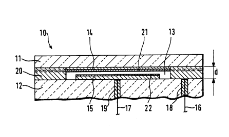
The pressure sensor 10 shown in Figs. 1 and 2 has a dia-
phragm 11 in the form of a circular disk with plane-
parallel surfaces which is joined around the periphery
to a circular substrate 12 in a defined spaced relation-
ship d, so that a chamber 13 is formed between the flat
top side of the substrate 12 and the opposite surface of
2031427
the diaphragm 11. The diaphragm 11 may be of ceramic,
glass, or a single-crystal material. The substrate 12
may be of ceramic, glass, or a single-crystal material,
too, but the materials of the diaphragm 11 and substrate
12 may differ. The diaphragm 11 is elastic, so that it
can deform when pressure is applied to it. The substrate
12 may be solid and rigid, but if desired, it may also
be a flat elastic disk like the diaphragm 11.
Those surfaces of the diaphragm 11 and the substrate 12
which face each other are provided with circular capacitor
electrodes 14 and 15, respectively, of metal which are
located opposite each other within the chamber 13 and spaced
a siven distance apart. The e~ectrode 14 completely covers
the diaphragm 11; however, it may also be provided only
in the area of the chamber. Each of
the electrodes 14, 15 is covered with a protective layer
21, 22. This protective layer is formed, for example,
from one of the oxides of the material from which the
electrodes are formed, as was mentioned above.
Connected to the electrode 14 and the conductive layer
15 are terminal leads 16 and 17, respect;ve~y, which are
brought out through the substrate 12 in a gas-tight manner.
The two electrodes constitute a capacitor whose capaci-
tance depends on the distance between the conductive
layers. When the diaphragm 11 deforms under pressure,
the distance between the two e~ectrodes changes, thereby
changing the capacitance of the sensor.-This capacitance
can be measured by means of an electronic circuit con-
nected to the terminal leads 16 and 17, and thus is a
measure of the pressure on the diaphragm 11.
2031427
This may be, for example, a pressure applied
to the pressure sensor from outside if the chamber 13
has been evacuated. On the other hand, the chamber 13 may
also communicate with the outside, e.g., through a hole
in the substrate 12, so that the pressure sensor can be
used as a reference-pressure sensor.
In a second embodiment of the pressure sensor, shown in
Fig. 3 in a schematic cross-sectional view, to prevent the
active solder of the active-solder inset 19 from skipping
to the capacitor electrode 14 of the diaphragm 11, the
endof the hole on the chamber side has a flare 23, which
receives the active-solder inset 19. Thus, when the
active solder becomes liquid, capillary attraction, which
would otherwise cause the active solder to grow beyond
the electrode plane of the substrate 12, is prevented.
The flare-23 thus acts and serves as a capillary stopper.
In a third embodiment of the pressure sensor, shown in
Fig. 4 in a schematic cross-sectional view, the sub-
strate 12 has two spaced-apart, concentric capacitor
electrodes 15, 15'; the electrode 15' thus encircles the
electrode 15, which forms a circular area at the center.
In the same way as the electrode 15 is covered by the
protective layer 21, the additional electrode 15' is
covered by an additional protective layer Z1'. Contact
is made to the additional electrode 15' by the addi-
tional active-solder inset 19'. This structure, using two
capacitors having a common electrode, namely the elec-
trode 14 of the diaphragm 11, may also be used in the em-
bodiment of Figs. 1 and 2, of course.
2031427
In Fig. 4, the hole for the additional active-solder in-
set 19' has, at its end on the chamber side, a f~are 24,
too, which has the same effects and advantages as the
flare 23. In Figs. 3 and 4, the termina( leads at the
active-solder insets 18, 19, 19' have been omitted for
the sake of simplicity.
In the finished pressure sensor, contact is made to the
diaphragm electrode 14 via the active solder 20 of the
joint and via the terminal lead 16. The latter and the
terminal lead 17 are contacted by the act;ve-solder in-
sets 18 and 19, respectively. The active-solder inset 19
extends to the substrate electrode 15, and the active-
solder inset 18 extends to the active solder 20 at the
joint and is thus connected to the dia~hragm electrode
14. The latter is indicated at the joint by a dashed line.
In a preferred embodiment of the invention, the capacitor
electrodes 14, 15, 15' are made of tantalum, and their
protective layers 21, 22, 22' of tantalum pentoxide.
A pecu(iarity of the pressure sensor shown consists in
the way the diaphragm 11 and the substrate 12 are joined
together. This is-done by means of a ring-shaped part of
active solder 20, which establishes the connection be-
tween the diaphragm 11 and the substrate 12 and also serves
as a spacer by ho(d;ng the diaphragm 11 at a def;ned dis-
tance d from the substrate 12. To establish the connection,
use is made of a thermal process which permits the dia-
phragm 11 and the substrate 12 to be joined directly to
the active solder 20 without previous metallization of the
nonmetallized portion of the substrate 12 and without the
use of a flux. Thus, an extremely strong and gastight
2031~27
joint between the diaphragm 11 and the substrate 12 is
obtained by means of the ring-shaped part of active
solder 20, so that the chamber 13 is hermetically sealed
from the surrounding atmosphere.
Active solder is a solder which contains at least one
strongly reactive element, such as titanium, zirconium,
beryllium, hafnium, or tantalum. During the soldering
process, these reactive elements wet the surfaces of the
parts to be soldered. If these parts are made of oxide
ceramic, the high affinity of the reactive elements for
oxygen wil~ cause a reaction with the ceramic, which leads
to the formation of mixed oxides and free chemica~s valen-
ces. The reactive component of the solder is embedded in
a matrix of other alloying elements, such as silver/copper.
Theseform the soldering material proper.
Ductile active-solder alloys contain 1 to 5% titarium,
which is homogeneously embedded in a matrix of, e.g.,
silver/copper. These alloys can be formed like normal
brazing solders into parts of any shape and, thus, into
the ring-shaped part shown in Fig. 2, which serves as a
spacer
Typical commercially available active solders are the
alloys silver/titanium, silver/copper/titanium, and sil-
ver/copper/indium/titanium, whose soldering temperatures
range between 750 C and 1050 C Thus, step soldering
(gradations in the melting points) is also possible with
active solders. The strengths of active solders are iden-
tical with the strengths of comparable titanium-free
2031427
- 10 -
brazing solders. The bond strength to ceramic is greater
than the strength of the ceramic itself; in a tensile
test, the fracture will therefore lie in the ceramic,
not in the ceramic-to-solder interface.
The soldering of the ceramic parts by means of the active
solder is preferably carried out in a vacuum at at least
10 5 mbars, better in the 10 6-mbar range. ~ery good
vacuum is necessary in order to avoid reactions of the
titanium with the residual gas and achieve good wetting
of the ceramic.
To obtain specific soldering results, e.g., to reduce the
evaporation of the solder or to reduce surface oxides,
it may be advantageous to carry out the heating or sol-
dering process in a defined gas atmosphere of inert gas
and/or reactive gas. The partial pressures of these gases
are preferably below 10 mbars.
During active soldering, as during conventional soldering,
the solder is completely melted through. The soldering
temperature of the active solder, however, shou(d be
30C to 100C above the liquidus temperature to obtain
an optimum reaction of the titanium with the ceramic.
In this manner, high strength and vacuum tightness a-re
achieved.
Besidesthese ductile active solders, brittle active sol-
ders can be used in the invention. To the inventor's sur-
prise, he found that during thermal-shock cycles, the
properties of the pressure sensor were not changed des-
2û31~27
pite differences in the coefficients of expansion of thediaphragm/substrate material and the brittle active sol-
der. Brittle active solders are composed of 30% to 60%
copper and a remaining percentage of zirconium, or 24%
nickel and 76% zirconium, or 36% to 7~% copper and 64% to
25% titanium, for example. These active solders must be
applied in the form of sintered rings or solder paste be-
tween substrate and diaphragm.
Preferably, the active-solder rings may be formed by the
so-calledmelt-spinning technique, whereby the solder is
first produced in amorphous form as a ductile foil. Thus,
it is readily machinable and can be given any shape. After
the soldering process, the solder is given its crystalline
properties.
As measurements show, the properties of pressure sensors
using such brittle active solders as joining materials
are not changed by thousands of thermal-chock ~ycles
between -20C and ~140C. In particular, no hairline
cracks are formed which - if vacuum tightness is inten-
ded - would make the chamber leaky.
Examination of the joint shows no changes in structure.
Since brittle active solders can be used, too, there is a
wider ran~e of materials for the diaphragm/substrate and
active solder to choose from than before.