Note: Descriptions are shown in the official language in which they were submitted.
CFO 7257 CA
2031733
-- 1 --
1 METHOD FOR FORMING PROBE AND APPARATUS THEREFOR
BACKGROUND OF THE INVENTION
Field of the Invention
The present invention relates to a method for
forming a probe of an information reading and/or input
apparatus, and an apparatus therefor. Such information
reading and/or input apparatus is utilized, for example,
in a surface observing apparatus such as a scanning
tunnel microscope (STM), a high-density record/reproducing
apparatus capable of recording and reading information
in the size of atomic order (several Angstroms), an
encoder for fine positioning, measurement of dimension
or distance, positional measurement for speed measurement,
particularly measurement and control requiring a resolving
power of atomic order, or the like.
Related Background Art
Recent development of the scanning tunnel
microscope capable of directly observing the electronic
structure of the surface of a substance or in the vicinity
of the surface [G. Binnig et al., Helvetica Physica
Acta. 55, 726(1982)] has enabled to measure the real
space image with a high resolving power, both in the
monocrystalline and amorphous substances. Applications
Of a wide range are expected for such scanning tunnel
microscope, as it is usable for various materials, allow-
ing observation with a low electric power without damage
to the specimen by the electric current and being capable
20~1733
1 of functioning not only in high vacuum but also in air
or in solution.
The scanning tunnel microscope is based on a
current generated between a metal probe and a conductive
5 material when they are brought to a small distance about
1 nm, with a voltage therebetween. Said current is
very sensitive to the change in the distance of both
members, and the surface information of real space can
only be obtained by moving the probe in scanning motion
so as to maintain said current or the average distance
of both members constant. In such case a resolving
power of 1 A or less can be obtained in the direction
along the surface.
In the conventional ordinary scanning tunnel
microscopes, there is employed a method of detecting
the tunnel current flowing between the surface of
conductive specimen and the pointed end of the detecting
conductive probe (probe electrode), effecting electric
feedback control on the distance between the specimen
surface and the detecting probe so as to maintain a
constant tunnel current, and displaying the structure
of atoms and molecules as an image. The resolving power
of such scanning tunnel microscope is determined by
the radius of curvature of the pointed end of the probe.
For improving the resolving power, therefore, the pointed
end of the probe has to be made sharper.
On the other hand, the recording capacity in
2Q317~3
-- 3
1 data recording apparatus has been increasing year after
year, and such tendency calls for reduction in size
of the recording unit and increase in the density thereof.
For example, in the digital audio disk utilizing optical
5 recording, the recording unit has been reduced as small
as about 1 ~m2.
The above-explained principle of the scanning
tunnel microscope can be utilized in realizing information
recording with a recording unit of 0.001 ~m2 or smaller,
by employing a material with memory effect for the
voltage-current switching such as a thin film of an
organic compound with ~-electron system or a charcogenide,
as the recording medium. An apparatus for high-density
information recording and reproduction with such recording
medium is generally equipped with a vernier control
mechanism or an X-Y stage for maintaining a probe electrode
at a small distance of about several nanometers to the
recording layer and mutually moving said probe electrode
and recording layer, in order to effect the recording
and reproduction in an arbitrary position in the recording
layer.
For achieving high-density recording and reproduc-
tion, there are required not only a recording medium
with small recording unit, but also a probe electrode
of which pointed end, governing the resolving power
in the direction of recording layer, sharpened to the
atomic or molecular level.
~ 4 ~ 2 03 1 q 3 3
l Thus, in an observing system such as the scanning
tunnel microscope for observing a specimen with a resolving
power of atomic order or in a high-density information
record/reproducing apparatus in the atomic order utilizing
5 the principle of such scanning tunnel microscope, the
pointed end of the probe electrode has to be made very
sharp.
For this reason, the probe electrode is generally
composed of a platinum or tungsten rod of which an end
is pointed in a conical shape by mechanical polishing
or electrolytic polishing.
However, in the actual operation of such surface
observing apparatus or information record/reproducing
apparatus, the pointed probe electrode may be brought
into contact with the information bearing member such
as the observed specimen or recording medium, as they
are maintained at a very short distance of several nano-
meters. Also in the operation in the air, the pointed
end of the probe electrode may be contaminated by the
dusts in the air. In such case the probe electrode
loses the resolving power of atomic or molecular level,
and there will result a loss in the resolving power
or recording density of the entire apparatus, in the
reliability and overall performance thereof. It therefore
becomes necessary to replace the probe electrode. The
replacement is made with a probe electrode formed in
advance by electrolytic polishing or electrolytic discharge
forming.
~ 5 ~ 2031733
1 However, such conventional method has been
associated with a drawback that the formed shape of
probe inevitably fluctuates, so that the resolving power
in the surface observation with the scanning tunnel
microscope or in the recording and reproduction of the
information record/reproducing apparatus varies depending
on each mounted electrode.
A third example utilizing a probe electrode
pointed to atomic order is the encoder mentioned above.
Conventional encoders have a reference scale
having positional or angular information and detecting
means for detecting said positional or angular information
by relative movement to said reference scale, and are
classified into several types, such as optical magnetic
and electrostatic capacitative encoders, by the systems
employed in said reference scale and detecting means.
Also as an encoder with resolving power of atomic
order, there is already known an apparatus for detecting
the amount of parallel displacement disclosed in the
Japanese Laid-open Patent Application No. 62-209302
and utilizing the basic principle of the scanning tunnel
microscope disclosed in the U.S. Patent No. 4,343,993.
Such encoder is equipped with a reference scale
for length and a probe positioned close to said reference
scale, and has a function of obtaining the current
generated between the reference scale and the probe
which are provided with a driving mechanism and encoding
- 6 - 2031733
1 thus obtained information on said current.
The probe for detecting the tunnel current in
said encoder is generally composed of a sharp needle
formed by known electrolytic polishing method. Also
5 mechanical polishing may be used for this purpose.
The performance of the probe with sharpness
of atomic order for detecting the tunnel current is
the heart of the encoder and is directly related to
the performance of the encoder. However, in order to
detect the tunnel current of pA - nA order generated
between the reference scale and the probe, the distance
therebetween has to be maintained as small as several
nanometers, so that there may result mutual contact
by eventual vibration of floor or noises. The pointed
end of the probe will be damaged by such contact and
will lose the ability of length measurement of the atomic
order. Also the replacement of such probe results in
the aforementioned drawback that the resolving power
varies for each probe mounted.
SUMMARY OF THE INVENTION
In consideration of the foregoing, an object
of the present invention is to maintain area stable
resolving power even after the replacement of the probe,
in the probe formation for an observing apparatus, an
information record/reproducing apparatus or an information
reading and/or input apparatus for information reading
_ 7 _ 203 17 33
1 and/or input with a probe on an information bearing
member such as an observed specimen, a recording medium
or a reference scale, thereby improving the precision
and stability of such apparatus.
Other objects of the present invention will
become fully apparent from the following detailed descrip-
tion of embodiments of the present invention.
BRIEF DESCRIPTION OF THE DRAWINGS
Fig. 1 is a schematic view of surface detecting
means utilizing a fine probe of the present invention;
Figs. 2A and 2B are schematic views of a minute
projection formed on the end of the fine probe of the
present invention; and
Figs. 3A and 3B are schematic views showing
another method for forming the minute projection on
the end of the fine probe of the present invention.
DESCRIPTION OF THE PREFERRED EMBODIMENTS
Now the present invention will be clarified
in greater detail by embodiments thereof shown in the
attached drawings.
1st embodiment
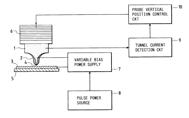
Fig. 1 schematically shows the structure, includ-
ing the electric block diagram, of a first embodiment
of the present invention. There are shown a conductive
probe 1 composed for example of tungsten, platinum,
2n~l733
-- 8
1 platinum-rhodium or platinum-iridium and pointed at
an end by electrolytic or mechanical polishing; a
conductive probe covering 2 composed of a conductive
material deposited for example by sputtering or plating;
5 a conductive specimen 3; a minute projection (end of
probe) 4, formed as will be explained later on the end
of the conductive probe 1 covered with the conductive
probe covering 2; a substrate 5 for fixing the conductive
specimen 3; vertical position control means 6 for control-
ling the distance between the conductive probe 1 andthe conductive specimen 3; a variable bias power supply
7 for application of a bias voltage between the conductive
probe 1 and the conductive specimen 3; a pulse power
source 8 for varying the bias voltage; a tunnel current
detecting circuit 9 for detecting the tunnel current
between the conductive probe 1 and the conductive specimen
3; and a vertical probe position control circuit 10
for controlling the vertical position control means
6. In the present embodiment, for controlling the distance
between the probe and the specimen, the tunnel current
is utilized for detecting said distance, but there may
be employed other means such as interatomic force, magnetic
force or electrostatic force for this purpose. In the
following there will be given a detailed explanation
on the method for forming the minute projection in the
above-explained structure, with reference to Figs. 1,
2A and 2B.
9 2 0 31 733
1 The conductive probe 1 was composed of tungsten,
and was sharpened with ordinary electrolytic
polishing. The radius of curvature of the end of said
probe was about 0.1 micrometers. The surface of the
5 probe 1 prepared by electrolytic polishing was covered
with gold, with a thickness of about 10 nanometers,
by an ion beam sputtering apparatus. The conductive
specimen 3 was composed of a platinum evaporated film.
The vertical position control means 6 was composed of
a commercially available PZT element, with a displacement
of 1 ~m/1000 V. In the above-explained structure, the
covering 2 of the probe 1 and the specimen 3 were
maintained at a distance of several nanometers, by
detecting said distance with the tunnel current detecting
circuit 9, and sending an instruction signal from the
vertical probe position control circuit 10 to the control
means 6 according to the result of said detection. In
order to prevent eventual change in the distance between
the probe 1 and the specimen 3 due to external perturba-
tions such as temperature drift or external vibrations,an electric feedback control was applied to the vertical
probe position control circuit 10 and the vertical position
control means 6, according to the output of the detecting
circuit 9. The apparatus was placed in the air. In
this state a pulse of a duration of 4 microseconds and
a height of 4 V was supplied from the pulse source 8
to the variable bias voltage source 7 supplying a positive
2031~73~
-- 10 --
1 voltage to the probe, thereby forming a minute projection
4 as shown in Fig. 1 or 2B, with a height of about 10
nm and an area of about 15 nm2 at the base.
The materials for the probe, probe covering
and specimen are not limited to those explained above
but can be suitably selected, as long as the melting
point of the specimen is higher than that of the probe
covering.
Also the conditions of the pulse can be suitably
selected according to the size of the minute projection
to be formed, but should be so selected as not to damage
the probe covering and the specimen.
The formation of the above-explained minute
projection allows to provide a fine probe capable of
resolving a molecular state both in vacuum and in the
air. Also the selection of a suitable material not
causing damage to the specimen in the pulse voltage
application allows to easily regenerate, within the
structure of the scanning tunnel microscope, a minute
projection with a resolving power of atomic or molecular
level even for a probe which has lost its resolving
power by eventual contact with the specimen in the opera-
tion of the scanning tunnel microscope.
2nd embodiment
In the following there will be explained a 2nd
embodiment of the present invention, with reference
to Figs. 3A and 3B. This embodiment is different from
~31733
-- 11 --
1 the 1st embodiment only in the structure of the specimen
3, which is provided with a projection 31 with a pointed
end, prepared in advance by a suitable known method.
The method of forming the minute projection 4 is same
as in the 1st embodiment, but the presence of the pointed
projection 31 creates a more concentrated electric field,
at the application of the pulse voltage, in comparison
with the planar specimen. It is therefore possible
to obtain a minute projection 4 with a smaller radius
of curvature than that of the projection 4 obtained
in the 1st embodiment (Figs. 1, 2A and 2B).
Formation of a minute projection with a smaller
radius of curvature on the end of the conductive probe,
by applying a voltage between said probe and a conductive
substrate while they are maintained at a small mutual
distance, provides an effect of higher resolving power,
due to said smaller radius of curvature.
The above-explained embodiment allows to form,
on the end of a probe with a pointed end of a radius
of curvature of 0.1 microns, a minute projection of
an even smaller radius of curvature in a simple process
by means of an apparatus of the structure of a scanning
tunnel microscope either in vacuum or in the air, thereby
providing a fine probe with a resolving power of atomic
or molecular level with a simple method, and being there-
fore greatly effective in the improvement of performance,
compactization of manufacturing apparatus and
20317~3
- 12 -
1 simplification of manufacturing method.
As the probe formation is achieved by voltage
application after detection and control of the distance
between an electrode and the location of probe formation,
5 the distance; at the probe formation can be precisely
controlled and a desired form can be precisely obtained.
The voltage application with a stably constant distance
provides constant forming conditions, thereby enabling
to obtain a constant shape in the formed probe.