Note: Descriptions are shown in the official language in which they were submitted.
203~
Patent
PD90-0033
High-Density ~emory Array Packaging
~ield of the Invention
The invention relates generally to a method an~
apparatus for high-density memory array packaging and,
more specifically, to a packaging technique having a
circuit board populated on both sides with high-density
multichip memory modules.
Background of the Inv~ntion
Advances in modern semiconductor fabrication
technologies have impacted the computer industry and
increased the demand for higher speed, lower cost, and
higher density computer systems. The sizes of
integrated circuit (IC) features have been reduced to
approximately 1 micron, thereby facilitating an increase
in the scale of circuit integration. Nowadays, the
function of a computer's central processing unit (CPU)
can be implemented on a single IC chip, making possible
computer systems that operate at high speeds. In order
to maximize the benefit of such chip
- . . .
. .' ~ ' .: .' :
,
" ~ ~ ,',' '' .
-: "'' ~ ,, .
. 203~65
level capabilities, the performance of a memory
subsystem must closely match that of the computer and,
more specifically, that of the CPU.
The size and cost of the memory subsystem are major
factors in the price/perEormance of the computer system.
The maximum size of main memory is generally limited by
the addressing capability of the CPU. With the
development of high performance CPU chips, fast and
large memory capabilities are required. However, modern
random access memory devices or RAMs are relatively
expensive and may constitute a large percentage of the
total computer system size. Accordingly, high-density
memory array packaging techniques are desired,
particularly ones that can utilize older, less expensive
memory chip technology without requiring redesign of
existlng computer platforms or cabinets. In some cases,
high-density memory packaging may necessitate
redesigning of computer platform/cabinet elements such
as the backplane, due to violation of spacing
requlrements, or the co~ling system, due to an inability
to remove heat from the high-density packages.
Another requirement of main memory is a high speed
interconnection between the RAMS within the main storage
subsystem and the CPU chips, since such off-chip
interconnection is a limiting factor in realizing
203~ 8~
overall system performance. Memory devices, in general,
are bus-oriented, thus making the interconnection
between main memory and the CPU less complex and less
prone to error. Nevertheless, the interchip
interconnection stratagy of the
RAMs must minimize the contribution of added inductances
and stray capacitances, so as to avoid decreasing memory
subsystem performance.
The present invention, provides a new and improved
method and apparatus for high~density memory array
packaging which results in a larger and more economical
memory subsystem.
The invention in its broad form resides in
apparatus for providing a low-profile, high-density
package for integrated circuit chips, said apparatus
configured for insertion into a computer backplane
having a plurality of equally spaced connectors with a
predetermined distance between adjacent ones of said
connectors, said connectors being configured for
receiving a plurality of adjacent boards, said apparatus
comprising:
a circuit board having electrically conductive
portions on a first surface and a second surface, said
circuit board being further configured for insertion
2~186~
into a connector of said backplane;
at least two generally planar multichip modules,
each having a first side and a second side, each of said
multichip modules having low profile integrated circuit
chips mounted to said first and second sides thereof in
conductive relation with electrically conductive
portions on said first and second sides;
edge connection means for mechanically connecting
one of said at least two multichip modules to selected
points of said conductive portions of said first surface
of said circuit board and another of said at least tWG
multichip modules to selected points of said conductive
portions of said second surface of said circuit board,
with said connection means being configured, dimensioned
and arranged for providing electrical connections from
said selected points of said
-3A-
203 l~
conductive portions of said circuit board to selected
points of said conductive portions of sa;d first and
second sides of said multichip modules; and
thermal means for managing the thermal loads
created by said low-profile chips, said thermal means
distributing the thermal loads by activating and
deactivating said low profile chips in a pattern that
avoids undue concentration of thermal dissipation such
that said thus-assembled, low-profile package is capable
of insertion into said backplane connector without the
need of redesigning to change said predetermined
distance to accommodate adjacent boards in connectors of
said backplane.
A preferred embodiment of the present invention
provides a low-profile, thermally managed, high~density
memory array package such that the memory array package
may be inserted into a standard computer backplane
without the need for redesign of the backplane or
computer cooling system due to violation of spacing
requ~rements or cooling specifications.
A modification provides a high-density multichip
module interconnecting memory chips on a multilayer
interconnect member to a circuit board, thereby
increasing the performance and density of the memory
subsystem.
Yet another modification of the present invention
-~B-
.
., ~
2~3~5
provides a new and improved method and apparatus for
high-density memory array packaging that integrates less
complex, higher yielding and less e~pensive RAM devices
on an interconnect member.
-3C-
:
~ `
2~3~
1 Su~0a~y o the Inventio~
3 The foregoing and other features of the invention are
4 accomplished by providing a low-profile, high-density
S package for IC chips, the package bein~ configured for
6 insertion into a computer backplane having connectors at a
7 predetermined equally spaced distance between each other.
8 In general, a first multichip memory module i9 provided for
9 high density packaging of IC chlps to a circuit board. A
first multilayer interconnect member is constructed having
11 a first side and a second side with the first side having
12 electrically conductive portions for transmitting and
13 receiving electrical signals. Low-profile memory chip~
14 are then mounted on the first side in conductive relation
with the conductive portions. Likewise, a second
16 multilayer interconnect membcr is constructed having first
17 and second sides w`ith the first side having electrically
18 conductive portions for transmitting and receiving
19 electrical signals.- Low-profile memory chips are mounted
on its first side in conductive relation with the
21 conductive portions. The second side of the second member
22 is thereafter affixed to the second side of the first
23 member, and low-profile edge clips are subsequently applied
24 to electrically and mechanically connect the conductive
portions on the first sides of the members to respective
26 conductive portions on a first surface of a circuit board.
27
28 A ~cond multichip memory module is also provided, the
29 second ~ultichip memory modula including first and second
muleilayer interconnect members constructed in a manner
31 similar to that described above. Low-profile memffry chips
~ 2~3~
are mounted to the first sides of the members again in a
manner similar to the first multichip memory module
described above. The second sides of the members are
joined together and low-profile edge clips are
subsequently applied to electrically and mechanically
connect the conductive portions on the first sides of
the members to respective conductive portions on a
second surface of the circuit board. A thermal
management technique that distributes thermal loads is
thereafter applied, thereby creating a high-density
package capable of insertion into a standard computer
backplane connector.
In an alternative embodiment of the invention,
low-profile memory chips are mounted to a first and
second side of each of at least two interconnect
members, the interconnect members having electrically
conductive portions on their first and second sides.
The memory chips are mounted in conductive relation with
the conductive portions of the interconnect members.
Low-profile edge clips are used to mechanically and
electrically connect one of the interconnect members to
a first surface of a circuit board and another of the
interconnect members to a second surface of the circuit
board. The thus-assembled package is then capable of
insertion into a standard computer backplane without the
need for redesign.
-5--
.
. . ..
. : : .
203186~
Other objects, features and advantages of the invention
will become apparent from a reading of the specification
when taken in conjunction with the drawings, in which
like reference numerals refer to like elements in the
several views.
-5A-
', ' ' ` ~ ' ~
~3~8S~
BrieE Description of the Dra~in~
A more detailed understanding of the invention may
be had from the following descrip~ion of a preferred
embodiment, given by way of example and to be understood
in conjuction with the accompanying drawing wherein:
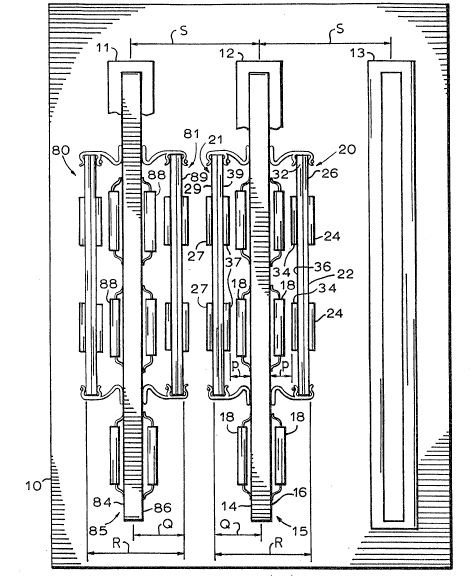
Figure 1 is a front diagrammatic view of a computer
backplane housing a high-density memory array packaging
apparatus according to a preferred embodiment of the
invention;
Figure 2 is an exploded perspective view of the
high-density memory array packaging apparatus used in
the backplane of Figure 1;
Figure 3 is a front view of an embodiment of a
high-density multichip module used in the memory array
packaging apparatus of Figure 1;
Figure 4 is a cross-section view of a multilayer
interconnect substrate member used in the high-density
multichip module o~ Figure 3;
Figure 5 is a perspective view of an alternative
embodiment of the high-density memory array packaging
apparatus according to an embodiment of the invention;
.
~. : . , , . , ~
. , : ,, . . , , ~ . .
. . . . .
: ' ''~ ': , ' ~ ,
-- 2~318~5
and
Figure 6 is a front view of an alternative
embodiment of a high-density multichip module used in
the memory array packaging apparatus of Figure 5.
Description of the Preferred ~mbodiments
Referring to the drawings, and particularly to
Figure 1, there is shown a front plan view of the
in~erior of a computer backplane 10, whch is of the type
installed in a
-6A-
.
.
,
.
2~3~ 86~
typical computer enclosure or cabinet (not shown). The
backplane 10 is a conventional backplane which includes
a plurality of adjacent, equally spaced edge connector
receptacles 11-13 that define, in part, backplane slots
(not shown). Each connector 11-13 is configured for
receiving a circuit board capable of insertion into a
backplane slot that typically measures a distance S in
the range of 12.5 to 25mm (0.5 to 1.0 inches) from the
center of one connector 12 to the center of an ad~acent
connector 11,13. Two adjacent circuit boards are shown
in Figure 1 and have been designated generally by the
reference numerals 15,85.
Circuit board 15 (85) is, for example, a printed
wiring board of the conventional type, that is a
generally rectangular, generally planar, plate-shaped
member having an electrical edge connector portion on
one edge thereof (not shown) for insertion into one
connector 12 or slot of the backplane 10. Circuit board
15 consists of an insulative substrate material having
conductivve lamina on two major, opposite surfaces 14,16
thereof, with selected portions of the condutive lamina
removed to define conductive paths assembled on the two
major surfaces. Circuit board 15 may also have numerous
/
. : . ; ,:
., ~:.: ,'
' .
-` 203~8~ 1
internal conductive and non-conductive layers sandwiched
between the outer, opposite surfaces 14,16.
Referring now to Figures 1 and 2, there is
illustrated an embodiment of the high-density packaging
apparatus of the present invention whereby circuit board
15 is populated on both surfaces 16,14 with
surface-mount electronic components including IC devices
or chips 18. Two multichip
-7A-
.. ,.;.......... ..... ~
2~3~
1 memory modules ZO,21 are also shown in relation thereto.
2 It is ~o be understood that the invention is equally
3 applicable to a high-density packaging apparatus that does
4 not have electronic components surface-mounted directly to
the surfaces 16,14 of circuit board 159 but that is
6 populated with one or more multichip moduleg 20,21 on both
7 surfaces 16,14. Yet, the embodiment shown in Figures 1 and
8 2 will be used ~o exemplify, among other things, the
9 thermal management issues associated with such packaging
apparatus.
11
12 The elements in Figures 1 and 2 (and Figures 3-6) are
13 somewhat exaggerated and are not drawn eo scale for
14 purposes of ease of depiction and ease of description.
Specifically, no attempt has been made to depict the total
16 number of chips mounted on the circuit boards or
17 multichip memory ~odules, or the scale size of the chips
18 and modules connected to the circuit board, although the
19 drawings depict the relationship relative to one another.
21 Mounted on both surfaces 16,14 of circuit board 15 are
22 a plurality of electronic components including IC chips 18.
23 Each chip 18 may be either a passive device, or a very
24 large scale integration (VLSI) or ultra large scale
integration (ULSI) active device fabricated with one of a
26 number of different technologies, such as
27 metal-oxide-semiconductor (MOS). It will be apparent to
28 thos~ skilled in the art that other technologically similar
29 IC chip3 may utilize the teachings and advantages of the
inventive concepts described herein; however, for an
'
2~13186~
.-
~
embodiment of the present invention, such devices areeither statlc random access memory (SRAM) or dynamic RAM
(DRAM) chips 18.
The DRAM chips 18 are mounted in conductive
relation to the conductive portions of circuit board 15
using known surface mount techniques and packages, some
examples of which are Very Small Outline Package (VSOP),
Thin Small Outline Package (TSOP), and packages
resulting from the Tape Automated Bonding (TAB) process.
These packaging technique~ are referred to as
"low-profile" chip packaging technologies, that is, the
height of the packages, which typically measures less
than 11.25 cm (0.045 inches), is much smaller than
conventional Small Outline J-Lead (SOJ) packages, which
typically measure 3.75 mm (0.15 inches). Low-profile
chip packaging allows for double-sided, surface-mounting
of components on circuit boards without violating
conventional backplane slot spacing requirements.
In accordance with the teachings of the invention,
a low-profile, high-density memory packaging apparatus
is provided, such apparatus including a first
high-density, multichip memory module 20 mounted to the
surface 16 of circuit board 15, the module 20 including
chips 24 mounted to a side 26 and chips 34 mounted to a
side 36 thereof. Likewise, a second high-density,
2~3.~86~
,
multichip memory module 21 similar to module 20 is
mounted to the surface 14 of circuit board 15, the
module 21 including chips 27 mounted to a side 29 and
chips 37 mounted to a side 39 thereof. Multichip
modules 20.21 are configured, arranged and positioned in
a manner generally parallel to and in proximate relation
to the surfaces 16,14 of circuit board 15, that is, the
distance P between the surfaces 16,14 of
-9A-
,
203~65
clrcuit board 15 and the closest portions of modules20,21 ln facing relation to circuit board 15 is
generally equal and in the range of approximately 1.25
to 2.5 mm (o.050 - 0.100 inches).
Referring only to Figure 1 at this point, circuit
board 85 is shown inserted into connector 11 of
backplane 10 and adjacent to the high-density memory
packaging apparatus of circuit board 15. Adjacent
circuit board 85 is populated with chips 88 and
multichip memory modules 80.81 in a manner similar to
that described for circuit board 15, and therefore
provides, in accordance with the teaching of the
invention, another high-density memory packaging
apparatus. A feature of the present invention is to
provide a low-profile, high-density memory array package
such that the package can be inserted into standard,
conventional computer backplanes having spacing
requirements that typically measure, worst case, a
distance S which is approximately 12.5 mm (0.5 inches)
from the center of one connector to the center of an
adjacent connector. In accordance with this feature, the
relativé dimensions of the fully populated, high-dansity
memory packages of circuit boards 15,85 are compatible
with the above-stated spacing requirement and as such
allow insertion of both packages into adjacent
connectors of conven~ional backplanes. In other words,
IB
2~31~5
,
the width R of circuit board 15 (85) having at least two
populated multichip modules 20,21 (81.80) mounted to
surfaces 16.14 (86,84) thereof respectively is
approximately 9 mm ~0.360 inches) or, stated
differently, the distance Q from the center oi circuit
board 15 (85) to furthest point of surface 29 (89) of
multichip module 21 (81) in facing relation to each
other is 4.5 mm (0.180 inches). These dimensions are
well within the 12.5 mm (0.5 inches) spacing requirement
of conventional backplanes.
-lOA-
- ~ '
: ~ '
~3~
1 In Pigure 3, the high-density multichip memory module
2 20 o~ Figure 2 i3 shown, the multichip memory module ZO
3 including a plurality of multilayer interconnect members
4 22,32 ha~lng conductive portions 25,35 on sides 26,36
thereof, the conductive portions 25,35 interconnecting a
6 plurality of chips 24,34, which preferably use silicon as
7 the semiconducting material. Multilayer interconnect
8 member 22 (32) is a generally rectangular, generally planar
9 member consisting of a plurality of conductive and
non-conductive layers deposited upon a base of substrate
11 material, as will be further described. In order eo
12 achieve high-density interconnections, multilayer
13 interconnect member 22 is constructed in a manner different
14 from traditional printed wiring boards, that is, the
multilayer member 22 is generally produced using thln-film
16 and lithographic techniques similar to those used in
17 semiconductor fabrication. This results in a multilayer
18 interconnect having substantially finer conductor lines and
19 thinner insulating layers than conventional printed wiring
boards.
21
22 Chip 24 (34) is a ULSI chip fabricated with MOS
23 technology and, for the instant invention, is a DRAM chip,
24 although similar IC chips may be used in accordance with
the teachings set forth herein. DRAM chip 24 is also
26 preferably a "bare" DRAM chip, that is, the chip 24 is not
27 housed ~ithin a certain IC package or by a certain IC
28 packaging technlque. Bsre DRAM chip 24 and multilayer
29 interconnect member 22 are individually and separately
tested prior to assembly, the chip 24 being assembled to
'~ ~
-~ 2.03~ 86~ ~
1 the multilayer membee 22 utilizlng bare chip assembly
2 technolo6y, an exampl~ of which is a technique known as
3 "flip-chip" bondlng.
As can be seen in the drawing, a side 2~ of the
6 multilayer interconnect member 22 is ~oined to a side 3a of
7 multilayer interconnect member 32 to form the hlgh-density
8 multichip memory module ~0, the multichip module 20 having,
9 as a result thereof, a plurality of chip mounting sides
26,36. The sides 28,38 are preferably affixed by an
11 adhesive substance, such as electronic grade epoxy,
12 althou~h those skilled in the art will recognize that other
13 similar, suitable techniques may be used to join the side~
14 28,38 together in abutting relation, for example with the
use of mechanical edge clips.
16
17 In accordance with the teachings of the invention9 the
18 high-density multichip memory module 20 i9 coupled to
l9 circuit board 15 by edge connection means, a specific
example of which ~re edBe clips 30. Edge clip9 30 are
21 configured, dimensioned, and arranged to provide electrical
22 connections from conductive portions 19 o~ circuit board 15
23 eo selected, conductive portions of side~ 26,36 of members
24 22,32, such as conductive portions 25,35 respectively. The
electrical connections between edge clips 30 and conductive
26 portions 25,35 of interconnect members 22,32 are
27 established by conventional soldering means, ~hile the
28 electrical connections between edge clips 30 and conductive
29 portlons 19 of circuit board 15 are established by
conveDtional surface-mounting means.
31
.32 Edge clip 30 also provides.mechanical coupling and
33 structural support between multichip module 20 and circuit
34 board 15, ~hile providing a "low-yrofile" to the
-12-
203186~
high-density multichip module 20. In fact, the height T
of a multichip module 20 populated with chips 24,34 on
both sides 26,36 thereof is approximately 3.3 mm (0.130
inches) which is less than conventional SOJ packages,
while the height V of the multichip module 20 coupled
with edge clip 30 is approximately 4.5 mm (0.180
inches). A low-profile edge clip found to be
satisfactory in the apparatus of the present invention
is shown and described in U.S. Patent No. 4,592,617
issued to Jack Seidler on June 3, 1986.
Referring now to Figure 4, the multilayer
interconnect member 22 of Figure 3 is illustrated, the
interconnect member 22 being a generally rectangular,
generally planar member consisting of a plurality of
conductive layers 44 and insulative layers 46 deposited
upon a substrate layer 40. The substrate layer 40 forms
the base of multilayer interconnect member 22 and, as
such, has a top side 42 and a bottom side 41 and a
length equal to the length of member 22. Substrate
layer 40 may be constructed of any of a number of
suitable substrate materials such as ceramic or metal,
but for this partlcular embodiment, silicon is the
preferred material due to its good thermal conductivity.
The use of silicon also minimizes thermal mismatch when
soldering the bonding pads 23 of the chips 24 to the
silicon substrate layer 40 of member 22. In other
- J3--
2~31~5
words, by using similar materials, for example silicon
for both the bare chips 24 and substrate layer 40, the
possibility of thermal mismatch is less, thereby
preserving the
-13A-
- . '
` ~3~81~
1 integrity of the solder bump ~oint 4U which would otherwise
2 bQ dao~g~d due to thermal expangion at different rates if
3 di~si~ilar matarials were used.
~,
Disposed upon the top side 42 of the silicon substrate
6 layer 40 are a plurality of layers of conductor 44,
7 preferably constructed of either aluminum or copper
8 material due to their low resistivity, separated by a
9 plurality of layers of insulator 46. As will become more
apparent hereinafter, a feature of the present invention
11 lies in the reparability of the multichip memory module 20
12 or, more specifically, the ability to replace certain bare
13 chips 24 assembled ~o multilayer lnterconnect member 22
14 prior to encapsulation, such repair being a function of the
structure of the member 22, i.e. the building of the member
16 22 upon one side (slde 42~ of th~ substrate layer 40.
17 Polyimide is the preferred material for the insulative
18 layers 46 since it haq a lo~ dielectric constant and is
19 able to planarize the structure of the underlying conductor
patterns when applied by spinning or spraying, thereby
21 allowing for the fabrication of multilayer met~llic
22 structures without a step coverage problem.
~3
24 As previously mentioned, bare chip 24 is assembled to
multilayer interconnect member 22 using a technlque called
26 flip-chip bonding9 a preferred implementation of which is
27 solder bump. Flip-chip bonding involves positioning the
28 bare chip 24 face-down onto the side 26 of interconnect
29 me~r 22, alignin~ the bonding pads 23 of chip 24 to the
conductive portions 2S of member 22, and thereafter bonding
31 the pads 23 in conductive relation to the conductive
32 portions 25. Unlike conventional printed wiring boards,
33 multilayer interconnect member 22 is designed to
.
-14-
2 ~3~
accomodate the tight spacing or "pitch" between the
bonding pads 23 of chip 24. The pitch between bonding
pads 23 typically measures between 0.15 - 0.20 mm (0.006
- 0.008 inches)1 compared to the pitch between TSOP,
VSOP, and TAB package leads, which measures
approximately 0.5 mm (0.020 inches) and which can be
accommodated by conventional printed wiring board
technology.
Flip-chip bonding is desirable for high-density
chip packaging because the footprint or area required to
bond the chip 24 to the member 22 is equal to the area
of the chip 24 itself, unlike other low-profile
packaging technologies VSOP, TSO~, or TAB which require
a larger footprint. Flip-chip bonding exploits the use
of a relatively small solder bump 48, which typically
measures a height Y of approximately 0.0254 to 0.038 mm
(0.001 - 0.0015 inches) and a width Z of approximately
0.05 mm to 0.1 mm (0.002 - 0.004 inches), required to
bond the pad 23 of chip 24 to member 22. In addition to
allowing higher packing densities, the small solder bump
48 minimizes aded inductances and stray capacitances of
longer leads, thus improving signal integrity. Also,
since flip-chip bonding allows the mounting of a "bare"
chip 24 to multilayer interconnect member 22, the
bonding technique helps provide a low-provile height to
the multichip module 20, thus helping to reduce the
.
:. , ' : . ~' .
2~31 8~5
overall size and dimensions of the high-density
packaging apparatus.
In accordance with a feature of the invention, the
bare DRAM chip 24, once assemble to side 26 of
multilayer interconnect member 22, can be replaced and,
thus, the entire multichip memory module 20 can be
repaired prior to encapsulation with a suitable
packaging material, for example electronic grade epoxy
encapsulant. Repair may be
-15A-
- 2 ~ 3 ~
necesary at this point, notwithstanding that both chip
24 and multilayer interconnect member 22 were previously
individually tested, since, in some cases, pretesting of
the chip 24 at design speed is difficult. Therefore,
the possibility exists that chip 24 cannot meet design
speed specification or that chip 24 became defective due
to the bonding process. In any event, replacing such a
chip 24 bonded to side 26 prior to encapsulation is
economical in terms of time and cost since it is
necessary to reflow the solder on only one side of
member 22.
As mentioned previously, another feature of the
present invention is to provide a low-profile,
high-density memory array package such that the package
may be inserted into a standard computer backplane
without violating backplane slot spacing requirements.
Accordingly, the width of a fully populated memory array
package vertically inserted into a standard backplane,
that is a package including at least one fully populated
multichip memory array package vertically inserted into
a standard backplane, that is a package including at
least one fully populated multichip memory module
mounted to one surface of a circuit board and at least
one fully populated multichip memory module mounted to
the opposite surface of the circuit board measures
approximately 9.14 mm (0.360 inches) and is compatible
/~
- ~
2~3~8~
with conventional double-sided, surface-mount circuit
boards populated with SOJ device parkages7 thereby
allowing for the insertion of the memory array package
into a standard computer backplane.
Insertion of such low-profile, high-density
packages into a backplane also raises issues associated
with available power and cooling capabilities existing
within the computer cabinet. A further feature of the
invention
-16A-
203~ ~6~
1 lncludes a memory array package arranged in a manner that
2 distributes the thermal loads created by the hlgh-density
3 interconnection of aceive devices and chips. In other
4 words, such high-density packaging inherently includes more
devices and chips per unit area, which results in more
6 power dissipation per unit area. A preferred embodiment of
7 the invention utilizes DRAM memory chips having the
8 characteristics of operating in a high-power mode when the
9 chips are being accessed, such as during read/write
operations, or in a low-power mode when the chips are
11 retaining current state information. Accordingly, and
12 referring back to Figure 1, muleichip memory module 20
13 mounted to surface 16 of circuit board 15 is configured
14 such that chips Z4, which are bonded to slde 26, are in
high-power operation or "turned on", while chips 34 located
16 directly beneath and on the opposite surface 36 of
17 multichip memory module 20, are in low-power operation or
18 "turned off". Likewise, and in a similar application, th~
19 entire memory array package may be configured such that the
multichip memory module 20 is in high-power operation, that
21 is, chips 24,34 are turned on, while multichip memory
22 module 21, or more specifically, chips 27,37 are in
23 low-power operation or eurned off. Thls alternating
24 pattern of activating and deactivating certain memory chips
or "memory banks" depending upon their location is repeated
26 throughout the entire memory array package of multichip
27 modules, thus providing, in conjunction with available
28 computer resources, thermal management of the apparatu~ o~
29 the invention. Of course, it will be apparent to those
skilled in the art that other aceivatingtdeactivating
31 patterns may be employed without deviating from the
32 inventive concepts set forth herein.
-17-
- .
': .
~3~
,
1 In accordance with the teachings of the invention,
2 heat energy conduction o~ the multichip memory module ZO is
3 improved due to the method of encapsulating the DRAMs. The
4 encapsulation of bare chips 24 bonded to the multichip
memory module 20 at one time, that is, after the bonded
6 chips are tested, results in an encapsulant being applled
7 that i9 approxlmately an order of magnitude thinner than
8 the plastic molding material used to surround conventional
9 SOJ packages. Such encapsulation results in more efficient
power dissipation than conventional packaging.
11 '
12 This particular embodiment of the high-density
13 packaging apparatu~ of the present invention is capabl~ of
14 providing up to six times the memory density as compared to
conventional double-sided, surface-mount circuit boards
16 populated with memory devices. The inventors believe that
17 this additional feature of the invention overcomes a
18 limitation of conventional main memory subsystem packaging,
19 namely the need for larger and faster memory capabilities
commensurate with overall computer system size and improved
21 computer performance.
22
23 Figure 5 depicts a perspective view of an alternate
24 embodiment of the low-profile, high-density memory array
packaging apparatus. In accordance with the teachings of
26 the present invention, the high-density memory packaging
27 apparatus include~ a first high-density multichip memory
28 module 60 mounted to a surface 56 of a circuit board 55,
29 the module 60 including chips 64 mounted to a side 66 and
chip~ 65 mounted to a side 68 thereof. Likewise, a second
-18-
20318~
,
1 high-density multichip memory module 61, similar to module
2 ~0, ls mounted to a surface 54 of circuit board 55, the
3 mod~le 61 includlng chips 67 mounted to a side 69 thereof,
4 as ~ell as chips (not sho~n) mounted to an opposite side
(not shown) thereof. Multichip modules 60,61 are
6 configured, arranged and positioned in a manner generally
7 parallel to and in proximate relation to the surfaces 56,54
8 of circuit board 55, that is the distance between the
9 surfaces 56,54 of circuit board 55 and the closest points
of modules 60,61 to circuit board 55 is generally equal and
11 in the range of approximately 0.050 - 0.100 inches.
12
13 Circuit board 55 is similar to the circuit board 15 of
14 Figure 1 and, as such, is populated on both surface3 5~,56
with surface-mount electronic components including RAH
16 chips 58. Of course, the invention applies equally to a
17 high-density memory packaging apparatus that does not have
18 electronic components mounted directly to the surfaces
19 54,56 of circuit board 55. Chips 58 are mounted in
conduceive relation to the conductive portions of circuit
21 board 55 using known low-profile, surface mount techniques
22 and packages VSOP, TSOP, and TAB.
~3
24 The high-density multichip memory module 60 of Figure
5 is shown in Figure 6 and includes an interconnect member
26 62 having conductive portions lnterconnecting a pl~rality
27 of chips 64,65. In accordance ~ith this alternate
28 embodiment of the inven~ion, chips 64,65 are encapsulated
29 with~n lo~-profile packages TSOP, VSOP, or TA~.
Interconnect member 62, not having to accommoda~e the
31 limitations imposed by bare chip assembly technology, may
32 now be either a multilayer interconnect member similar to
-19-
2~3~8~
interconnect member 22 of Figure 4 or a conventional
printed wiring board. The chips 64,65 are therefore
assembled to the sides 66,68 of interconnect member 62,
respectively, using known surface-mounting techniques.
High-density multichip memory module 60 is coupled
to circuit board 55 using edge connection means, such as
edge clip 70. Edge clip 70, like edge clip 30 of Figure
3, is configured, dimensioned, and arranged to provide
electrical connection from conductive portions 59 of
circuit board 55 to selected, conductive portions 63,73
of sides 66,68 of member 620 The electrical connections
between edge clips 70 and conductive portions 63,73 of
interconnect member 62 are established by conventional
soldering means, while the electrical connections
between edge clips 70 and conductive portion 59 of
circuit board 55 are established by conventional
surface-mounting means.
Edge clip 70 also provides mechanical coupling and
structural support between multichip module 60 and
circuit board 55, while once again providing a
low-profile to the multichip module 60. In this
alternate embodiment of the invention, however, the
height X of multichip module 60 populated with chips
64,65 on both sides 66,68 thereof is approximately 4.19
mm (0.165 inches), which is compatible with
, . .- - - - - :
. ' : . . .
.
2031~5
1,
conventional, low-profile SOJ packages.
The thus-assembled alternate embodiment of the
high-density memory array packaging apparatus is capable
of providing between three and four times the memory
density of conventional double-sided, surface-mount
circuit boards populated with memory devices. The
distance V from the
-20A-
,:
~ .. , '
20318~
center of circuit board 55 to side 66 of multichip
module ~0 is approximately 4.95 mm (0.195 inches), which
also makes this alternate embodiment of the present
invention compatible with conventional computer
backplane spacing requirements. Additionally, the
alternating pattern of activating and deactivating
certain memory banks depending upon their location is
implemented throughout the entire packaging apparatus of
multichip modules 60,61 therefore providing thermal and
power management of existing computer system resources.
Uhile there has been shcwn and described preferred
embodiments of the present invention, it i5 to be
understood that other adaptations may be made within the
spirit and scope of the invention. One feature of the
invention lies in providing low-profile, high-density
packaging of memory array boards while obviating the
need for major connector level redesign of existing
computer backplanes. Another feature lies in providing
thermal management of the low-profile, high-density
packaging appaaratus, while again obviating the need for
major cooling system resdesign of existing computer
cabinets. Also, it is to be understood that although
the preceding description has proceeded with reference
to the high-density packaging of older memory chip
technology, the invention is equally applicable to newer
memory chip technologies and ULSI chip environments in
2~3~86~
general where high-densi~y chip packaging is
significant .
-2 lA-
1 It will therefore be apparene to those skllled in the
2 art that various changes and modificatlon3 in the
3 speclfically described embodiment~ can be carried out
4 ~ithout departing ~rom the scope of ehe lnventlon which i9
to be limited only by the scope of the appended claims.
-22-
:,. , , . . : .
,.
,
: -