Note: Descriptions are shown in the official language in which they were submitted.
2 ~ 3 1 & r~ ~
- MOBI LE ANTENNA SYSTEM
i3ACKGROUND OF THE INVENTION
Field of the Invention:
The present inventlon relates to an antenna system
for use in mobiles ~uch as motorcars and other vehicles and
particularly to such an antenna system that is suitable for
tracking dependent upon the moving direction o the moblle.
Description of the Prior Art:
With rapid pro~re~s of electronic communication
technlques, radiowave communication has been popular in
various ~ields. Particularly, wlth miniaturization of
electronic instruments such a~ transmitter-receivers and
others, the spotlight of attention is now focuse~ upon mobile
communication using a land mobile telephone or the like.
There is known a cellular mobile telephone sy~tem which
includes a plurality of ground base statlons. ~ach of the
base station~ controls the communication link between the
base station and mobiles within one area. This system has
been adopted in land moblle telephones and th~ e~ However,
such a communication s~stem utilizing the ground base
statlons can only be used in the limited area since the
number of base stations cannot inflnitely be increased.
Another mobile communication system is also known which
utilizes a communication satellite. The mobile ~atellite
communication system is being studied into practical use in
various applications since it does not have the
aforementfoned limitation as in the mobile communication
utili~ing the g~ound base stations and can do hi~h-quality
services over a wide area of a nation scale.
~3~872
In the latter case, an antenna to be mounted on the
mobile becomes one o~ very important factors. I~ the antenna
cannot well operate on transmission and reception, a
transmittsr receiver and associated electronic componen~s
cannot well ~unction even though the~ are very high in
performance.
As a mobile such as motorcar or other vehicle is mGving,
the direction of the satellite will vary every moment.
Therefore, the beam direction of an antenna mounted on the
mobile must be pointed to the satellite by use of any
suitable tracking means.
A step track method ls popular a~ tracking methods. The
step track method is adapted to maintain the beam direction
to the satellite by slightly moviny the direction of the
antenna at a suitable time interval so that the beam of
antenna is pointed in the direction o~ a received signal.
In such mobiles as ships and aircrafts which ~o not Yary
in direction very well and in which the blocking effect by
any obstruction does not risa, the 6tep track metho~ is
satisfactory on tracking the satellite.
However, land mobile~ are ~re~uently ~ teered and kurned
with higher speeds than those of the ships and alrcrafts and
radiowave from the satellite may be blocked by any obstruction
such as building or the like. ~herefore, it is frequent that
the step track method is not satisfactory in tracking~ Once
radiowave is blocked by a utility pole or building, the
mobile may miEs the satellite completely.
Even if radiowaves are being stably received b~ the
mobile, the strength of received signal may vary more than
neces~ary since the beam direction oE the antenna is always
g 7 ~:
change~ slightly every moment to search the maximum strength
of received signal.
The antenna must he as small and thln a~ po~sible since
it should be mounted on the mobile. And also, the antenna
must provide a low air resistance when the mobile i8 running.
Mechanically steered antenna cannot ~e miniatured since
it includes a mechanical drive.
A phased arra~ antenna is known which can be
electronically steered. Such a phased array antenna is
suitable for use in radar system and mobile satellite
communication. It is however difficult to mi~liature the
entire phased array antenna. Because it requires eeding
circuits including phase ~hifters, power dividers ~eedlng and
others control circuits for ~he phase shifters, and so on, in
order to contr~1 the atenna beam.
One of small antennas is a microstrip antenna which may
be utilized as an antenn~ element in an array antenna.
However, the micro~trip antenna has a disadvant~ge that it
has a narrow band width. In order to overcome such a
problem, there is considered a stacked microstrip antenna to
which a passive element is added to increase the band width.
To obtain the band width of 8~, the stacked micro~trip
antenna requires its height e~ual to about 0.075 wavelength.
When the central frequency is 1600 MHz, it is required that
the height of the antenna is about 14 mm. This is too high
for the intended purpose. As the antenna element is higher,
the mutual coupling is increased. As the result, it cannot
perform its function sufficiently in the gain and the axial
ratio.
SDK~ARY Ur ~l~ lNv~Nr
2 ~ ~ :L 8 rl 2
It is therefore an object of the pres~nt lnventlon to
provide an antenna system which has the following features:
(1) The beam of an antenna can be properly controlled
dependlng on the orientation of a moving mobile.
(2) The thickness of the antenna structure is so small
that it can easily be mounted in the mobile.
(3) The mutual coupling beteen antenna elements is so
small that it can sufficiently function as an array antenna.
(4) The good axlal ratio is obtained throughout the wide
frequency range.
To thls end, the present invention provides a mobile
antenna system which comprlses a phased array antenna havlng
an antenna elements layer, a feeding network layer and a
drive circuit layer, all of which are stacked one above
another, said antenna elements layer including a plurality of
radiating patch elements on a dielectric substrate, said
feedin~ network layer including a ~eeding network conslsting
of phase shiters and power dividers each of which is made
with microstrip-line and connected to the respective one of
said radiating patches, and sald drive circuit layer including
drive ~ircuits or controlling the phase ln each of the phase
shifter6; an angular rate sensor for detecting the turning
directlon of a mobile; a receiver for detecting the strength
of receive~ slgnals; and beam control means respon~ive to the
results of detection in the angular rate sensor and the
receiver for controlling the beam direction o ~aid antenna,
whereby the beam of the array antenna can be 3teered by
controlling the phase o~ each of said antenna elements
depending on the orientaion of the moving mobile.
In one aspect of the present invention, the feeding
~31872
network lncludinq the phase shifters and power dividers and
the drive circuit are arranged in th~ same face of the
substrate which is in turn stacked together with ~lat antenna
elements, permitting the entire thickne~s oE the antenna to
be very thin in comparison with the conventional phased array
antennas.
The on-vehicle tracking system of the present invention
has such a construction as described above. The phase
relative to each ~f the ant~nna elements in the array antenna
is controlled by a phase control section such that a
d~fferential phase between each adjacent antenna elements
will be set at a predetermined value. Thus, the pattern of
the array antenna can be controlled according to the antenna
element spacing and the differential phase.
Such an array antenna is called "phased array antenna".
This will be briefly described below.
There is now considered herein, for example, an array
antenna which comprises a plurallty o~ anteIIna elements Al to
An e~ual to n in number, these el~ments being arranged in
line at a space interval d, as shown in Figure 34. It is
also assumed that all the Antenna elem0nts A, - An are
isotropically radlatin~ elements. It is further presumed that
an angle included between the array antenna arrangement and a
normal line (angle of incidence) is ~ and that a plane wave
reaches when the angle ~ is equal to ~ O.
As~uming that the leftmost element Al as viewed in Figure
34 is a reference element, the phase of a wave reaching each
of the antenna elements A2 - A~ will advance by ~ ~ for each
antenna element from the starting element A2 to the ending
element An. Thus, ~ ~ is represented by:
1, 8 r~? 2.
~ ~ = 2~ (d/~ ) sin ~ O
where ~ is the wavelength o~ the incldenta:L plane wave.
If the phase in each of the antenna elements A2 - An is
delayed by ~ ~ by the phase shi~ters B2 - ~n and
thereafter they are combined together by a power combiner C,
high frequency si~nals can be -taken out in phase from the
respective a~tenna elements A, - ~". Therefore, the beam o~
the array antenna will be able to be scanned ln any
direction ~ .
On transmission, the radiated power is focused in any
direction ~ in the similar manner. I~ the antenna elements A
are arranged two-d~mensionally, the beam of the array antenna
can he scanned in three dimensions.
The present invention is to control the beam o the
antenna depending on the results of detectlon of the
orientation of the mobile during turning and the received
signal level from the recelver. When the mobile moves
stralght, the beam dire~tion o~ the antenna will not be
varied. Thus, the variations of recelvea ~ignal level can be
efectively suppre~sed. On turning, the beam dlrectlon of
the antenna is controlled to track the satellite well,
depending on the result~ of detection in the aungular rate
senæor and the received signal. When the radiowave i~ blocked
by any obstruction on ground, the tracking can be effectively
continued by using the angular rate sensor.
It will be apparent from the foregoing that the mobile
antelma system according to the present invention can
perorm the tracking very well slnce tracklng can be
controlled depending on the state of the moving mobile.
Furthermore, the mobile antenna system can ef~ectively deal
~3~87~
with any challge o~ mo-tion oE the mobile since the present
invention utilizes the phased arr~y antenna having the beam
which can electronically be controlled.
Since the phased array antenrla section comprises the
antennas, feeding networks and drive circuits which are
layered one above ancther, it can be formed into a thinned
structure which can be easily mounted on a small land mobile.
Microstrip antenna used as antenna elements in the array
antenna comprises a ground plane, a drlver patch elemento
disposed on a dielectric substrate opposite to the ground
plane and a parasitic driven patch element arranged and
spaced apart from the drlver patch element, the dielectric
substrate being formed into a stack of two or more dielectric
substrates having dif~erent dlelectric constants.
Thus, the microstrip antenna is characterized by that it
is formed into a dielectric substrate located between the
driver patch element an~ the ground plane, the dielectric
substrate being formed by a stack of two or more dielectric
materials having di~ferent dielectric constants.
In order to reduce mutual coupl1ng hetween antenna
elements, it is requlred that the spacing be-tween the
driven patch element and the ground plane is decreased. On the
other hand, if it is wanted to widen the band width, the
spacing between the driven patch element and the ground plane
must be increased. However~ the matching to the impedance of
the feed line cann~ be taken only by satisfying such
conditions, Therefore, the band width with low VSWR does not
become wide enough.
The inventors have studied such a problem ln rarious
types of experiments to research the condition required to
7 ~
take the matchlng. It has been thu.s found that the band width
of the antenna to be matched to the feed line .i9 changed hy
varying the relative dielectric cons-tant & , between the
dr~ver patch and the ground plane into the value & r ~ ~ ~
which can provide the maxi~um band width, as shown in Figure
35.
If tha relative dielectric constant is set to the value
of r ~ A X ~ the w~de frequency band width can be provided as
shown by solid line in Figure 22. If the resulting value &
rmnx iS equal to the value o r of a dielectric easily
available (which, ~or example, is equal to 2.6 for Teflon:
3.6 ~or a dielectric material comprising bis(maleimide)~
triazine resin and glass abric; and 4.6 for glass epoxy)~
such a dielectric material can be used to realize a wide
band antenna element.
It is frequent that the easily available dielectric does
not have its relative dielectric constant equal ~o the value
& rm~ -
In accordance with t~1e present invention, thus, the
microstrip antenna can have any specific inductive capacity
& r substantially equal t~ the value of & rm 8~ by stacking a
plurality o~ conventional dielectric materlals different in
dielectric constant from cne to another into a suitable
thickness.
For example, if a dielectric su~strate is formed by
stacking three dielectric layers having a thickness tl, t2
and t3 and relataive dielectric constants & r 1 ~ r 2 and
& r 3 repeatively, this substrate will have the entire
value of relative dlelectrlc constant & r rep~esented by:
& r = (tl ~ tl ~ t,)/
2~3~72
( tl / r ~ ~ t~/ ,z ~ t3 / r 3 ) ~
The required value ~ , can be equal to ~ r~ rl
accordance with the pre~ent invention, the substrate of the
driver patch element can haYe a widened ranye of the
dielectric constant by stacking two or more dlelectric
substrates different in relative dielectric constant from one
to another and also properly ad~usting the thicknes~ of each
substrate.
In such a manner, the microstrip antenna can have a
frequency band width which is increased up to about 8~. At
the same time, the spa~ing between the driven and driver
patch elemente can be reduced in comparison with the prior
art. Thus, if such microstrip antennas are u~ed as antenna
elements in the array antenna, the mutual coupllng between
the antenna element spacing can be redu~e~ and slmultaneously
the array antenna itself can be miniaturized with hiyher
function.
In accord~nce with the present in~ention, further, ~he
array antenna is characterized b~ that each of th~ antenna
elements has two ~eed points having dif~erent angles of 90
relative to the center and that said array antenna further
comprises feed means for supplyiny ~owers with 90 phase
difference to the two feed point of the antenna element to
excite the circular polarization, said antenna elements being
arranged into a triangle fashion and being rotate~ by 120
or feed positions different from each other by ~0 ~ .
In general, it is very difficult that only one of
antennas has a good axial ratio throughout the wide frequency
band.
An antenna is thus considexed herein whlch has a
8 r(~ 2
polarizatlon in the form of ellipsold as shown in ~i~ure 32.
It has been found that if two such antennas ~re arranged
perpendicular to each other, that i~, if the feed points are
arranged angularly rotated one another hy 90 to compensate
for the strength together, a good axial ratio can be obtained
as shown by broken line in Figure 33. It has been also
confirmed that a good axial ratio is provided over a wide
band width.
The a~ial ratio is further improved i~ the positions o~
the feed points are equally distributed in all the
directions. It has been further con~irmed that the location
of each adjacent antenna feed points at different positions
reduces mutual couplin~ between antenna elements.
If the ~eed points in each ad~acent antenna elements in
an array are differently positioned, the a~ial ratio in the
entire array antenna can be improved throughout a wide
frequency band. Even if each of antenna elements ha~
different feed po~ition, the antenna elements can be corrected
out of phase at di~ferent feed positlons to provide a
predetermined phase to each of the antenna element~.
The present invention ca~ provides a new and improved
array antenna comprising a plurality of antenna element~
having different feed point positions, which can lmprove it~
ax1al ratio and e~ectivsly perform the transmission and
reception over the wide frequency band.
BRIEF DESCRIPTION OF THE DRAWINGS
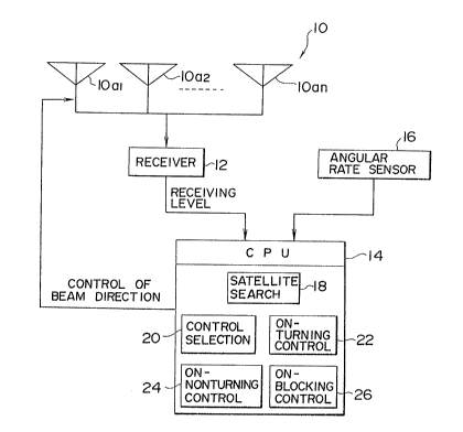
Figure 1 is a, schematic block diagram of one embodiment
of an antenna system constructed in accordance with the
present invention.
1 0
2 ~ 7 2
Figure 2 is a block diagram of a control selec~or section.
Figure 3 is a block d~agram o a turning control ~ection.
Figure 4 is a bloc~ ~iagram of a non-turning control
section.
Figure 5 is a block diagram o~ a radlowave blocking
control section.
Figure 6 is a flow chart illustrating the operation of
the antenna system.
Figure 7 is a flow chart lllustrating the sa~ellite
direction search (S2~ operation.
Figure 8 is a ~low chart illustrating the beam control
(S30) operation when the radiowaves are blocked.
Fiyure 9 is a 10w chart illustrating the beam control
(S40) operation when the mobile is movin~ straight.
Figure 10 is a flow chart illustrating the beam control
(S5~) operation when the mobile ls turning.
Figure 11 is a perspective view of a phasQd array antenna
in the first embodiment of the present invention.
Figure 12 is a perspective view of a phase shifter.
Figure 13 illustrates the operation o~ the phase shlfter.
Figure 14 is a perspective view of a power divider.
Figure 15 is a schematic cross-e~c~ion of the phased
array antenna in the first embodiment.
Figure lG is a cross-sectional view of the connectlon
between the phase shifter and a drive circuit in the first
embodiment.
Fi~ure 17 illustrates the COnneCtiQn of the drive circuit.
Figure 18 is a schematic cross-sectional view of a phased
array antenna in the second embodiment,
Figure 19 is a schematic cross-section of a phased array
2~31~7~
antenna in the third embodiment.
Figure 20 is a perspective vlew of the schematic
structure of a microstrip antenna relating to on~ embodiment
of the present invention.
Figure ~1 is a cross-se~tional view o~ the embodiment
shown in Figure 20.
Figure 22 is a graph showing variations o~ VSWR at the
antenna ~eed point relative to requencies in the embodiment
shown in Figures 20 and 21.
Figure 23 is a schematic top view of an array antenna to
which the principle o~ the microstrip antenna shown in
Figures 20 to 22 is applied.
Figure 24 is a graph showing variations of mutual coupling
between antenna elements relative to fre~uencies when
microstrip antenna elements accordlng to the embodiment shown
in Figures 20 to 22 are arranged in a plane.
Figure ~5 illustrates the arrangement of antenna elements
in the array a~tenna relating to the embodiment of the
present invention.
Figure 26 illustrates the position ot feed points to the
antenna elements i~ the ~ame embodiment.
F$gure 27 is a graph showi~g the a~ial ratio o~ the array
antenna in the same em~odiment.
Figure 28 illustrates a phase shift clrcult for supplying
power to the antenna elements.
Figure 29 illustrates a circuit ~or yenerating circular
polarization.
Figure 30 illustrates the position o~ the ~eed points to
antenna elements in another embodiment.
Figure 31 illustrates the arrangement o~ antenna elements
1 2
203~872
in still another embodime~t.
Figure 32 illustrates the polarization of an antenna
element.
Figure 33 illustrates the polariz.ation of a comhination
of antenna elements.
~ igure 34 illustrates -the principle of the phased array
antenna.
Figure 35 is a graph showing the relationship between the
relative dielectric constant and the band width.
DETAILED DESCRIPTION OF PREFERRED EMBO~IMENTS
Referring first to Figure 1, there is shown a mobile
antenna system constructed in accordance with one embodiment
of the present invention, whlch comprises an antenna 10
capable of being optionally controlled with respect to its
beam direction. This antenna 10 may be in the ~orm of a
phased array antenna, the beam dirsction of which can be
electrically controlled by using a phase shlfter. More
particularly, the antenna 10 may be a phased array antenna
comprising a plurality of antenna element 10al through lOan,
the number of which elements is equal to n in number.
Signals received by the antenna 10 are then ~upplied to a
receiver }2. The receiver lZ performs the conventional
signal processing operations such as detection, amplification
and others, with the resultant signals being then fed to the
conventional signal processing system. In this embodiment,
however, the receiver 12 is adaptea to g~ve the strength of
received signal (hereina~ter called "receiving level") to CPU
14.
In this embodiment, the t~rning detector section
rJ1 2,
comprises an angular rate sen~or 16 for detecting the
orienta-tion angle of the mobile, tha resultant data being
given to CPU 14. The angular rate sensor 16 ma~ be o~ any
one of various types such as ~as rate g~ro, vibrating gyro,
laser gyro, mechanical rate gyro and other~.
Although this embodiment will be de~cribed as to the
angular rate sensor, any other angle sensor such as
t~rrestrial maynetism sensor or the like may be used to
perform the similar control.
In response to the receiving level from the receiver 12
and the angle data from the angular rate sen80r 16, the CPU
14 controls the beam o~ the antenna 10. The CPU 14 comprises
five sections:
(a) Satellite Direction Search Secti~n
Satellite direction search section 18 is adapted to
search a direction of satellite by scanning the antenna
beam receptiun mode into the ominidirection and finding
the direction of the satellite in which the receiving
level become~ maximum. When the antenna 10 is controlled
by the satelllte direction search section 18, therefore,
the satellite can be ~ound from an initial state without
any information regarding to the satellite.
(b) Control Selector Section
Control selector section 20 comprises three parts,
that is, a receiving level reading part 20a, an angle
reading part 20b and a control selecting part 20c, as
seen from Figure 2. Dependin~ on the receiving level and
the orientaion angle of the mobile, the control selecting
part 20c selects optlmum one o~ three control parts, that
is, a turning control part 22, a non-turning control part
1 4
7 2
24 and a signal blocking csntrol part 26. In such a
manner, the antenna wlll be controlled.
(c) On-Turning Beam Control Section
On-turning beam control section 22 comprises an
angle reading part 22a, a receiving level reading part
22b, a turning direction judging part 22c, a left~hand
turning beam control part 22d, a right-hand turning beam
control part 22e and a phase shiEter control part 22f,
as seen from Fi~ure 3. The on-turning beam control
section 22 controls the beam of the antenna when the
vehicle turns. More particularly, the beam of the antanna
is moved to be directed to the satellite, depending
on data relating to the turn direction o~ the
mobile.
(d) On-Nonturnin~ Beam Control Section
On~nonturning beam control section 24 comprises a
receiving level reading part 24a, a beam control part 24b
and a phase shi~ter control part 24c, as seen from
Figure g. The on-nonturning beam control section 24
controls the antenna when ths vehicle is movin~ on gently
curved and straiyht roa~s. IE the vehicle is moving
straight or substanti~lly stralght, it is not basically
required to c~ange the direction of beam. Thus, the
on-nonturning beam control section 24 will only judge
whether or not thereceiving level is equal to or higher
than a predeterminedthreshold, while maintaining the
direction of beam constant~
(e) On-Blocking Beam Control Section
On-blocking beam control section 26 comprlses an
angle readlng part 26a, a r~ceiving level readlng part
1 5
2~3:187~
2~bt a turning angle computiny part 26c, a beam
controlling part 26d, a timer 26e and a phase shifter
control part 26f, as seen from Figure 5. The on-blocking
beam control section ~6 controls the antenna when
radiowaves are completely blocked by buildings or the
like. Since no signal is received ~y -the antenna in such
a situation, the direction of beam in the antenna lO will
be controlled by the information of the angular rate
sensor 16. The direction of the satellite can be
predicted from the in~ormation of the sensor 16. The beam
of the antenna 10 is directed to the known direction of
the satellite. However, this method may provide a wrony
value in the turning angle because of accumulating
angular errors. In order to avoid such a problem, the
beam ls scanned in the omnidlrectlo~al direction to
re-confirm the dtrectlon o~ the satellite after passage
of a given time period.
The control operation of the antenna 10 in this
embodiment will now be de~cribed with reference to Figure 6.
In the beginning of the operation, the satellite search
section 18 first judges whether or not the direction of the
satellite is unknown (Sl). Normally, the direction o~ the
satellite will be searched since it is unknown (S~).
When the satellite direction is known on termination of
the search (S2), the maximum receiving level and the
direction of beam are stored.
When the search oE the satellite direction ~S2) is
terminated or when the satellite direction has been known, the
beam is pointed toward that satellite direction (S3).
Next, the control selecting section ~0 selects one of the
1 ~
2~3:1~7~
on-turni~g beam control, the on-nonturning beam con-trol and
the on--blockiny beam confrol ~S5 ~ S10).
For this purpose, the recelving level reading part 20a
reads a receiving level LEV of a sign~l which is received
using the beam set at S3 (S4).
After obtaining a receiving leve LEV, switching level SL
and blocking level BL are determlned from the re~eiving level
LEV (S5) at the control selecting part 20c.
The switching lavel SL is a reference level used when the
direction o beam in the antenna 10 is to be switche~ in the
other direction. When a signal is received ln a certain
direction and if its receiving level LEV is lower than the
switching level SL, that beam is switched to an adjacent
beam. The blocklng level ~L is a level used when it is judged
that the radiowave is blocked. If the receiving level LEV is
lower than the blocking level TL, the tracking will be
performed using on the output of the angular rate sensor 16
wbich has been rea~ into the angle reading part 20b. It
should be determin~d that the ~witching level SL is the value
lower than the ma~imum recei~ing level LEVMAX by a given
a~ount and that the blocking level TL is substantially lower
than the maximum recelving level LEVMAX.
When the switching and blocking levels (SL and BL) are
determined through S4 and S5, these levels are used to
control the direction of beam of the antenna 10.
If the receiving level LEV is larger than the switching
level SL, this means that signal wi~h sufficient strength is
received in the current direction o beam. It is thus not
required to change the direction oE beam. When the receiving
level LEV is larger than the value of SL, therefore, the
l 7
~31~72
reading o~ the receiving level LEV and the comparison be-tween
the receiving and switchlng levels will be repeated.
1~ the receiving level LEV ls smaller than the value of
SL, the directlon of beam may be changed. It is thus judged
whether or not the receiving level LEV is smaller than the
blocking level BL (S8).
If the receiving level LEV is smaller than the value of
BL, it is judged that the radiowave fr~m the satellite is
blocked. The on-blocking beam control is thus carried out
(S30). Therea~ter, the process is returned to the receiving
level reading step (S6).
If the receiving level LEV is laryer than the blocking
level BL, it is judged that the radiowave is not blocked and
that the antenna beam is in the different ~irection. The
process rea~s the angle from the angular rate sensor 16 (S9).
From the comparison between the current and former angles,
it is ~udg2d whether or not the mobile is turning (S10).
If it is judged that the moblle is not turnlng, the
on-nonturning beam control is carried out (S~0). I~ the
mobile is turning, the on-turning beam control is performed
(S50). After these controls, the pxocess will return to the
receiving level reading step (S6).
The descriptlon will now be made individually to the
satellite search (S2), on-blocking beam control (S30),
on-nonturniny beam control ($40) and on-turning beam control
(S50).
Search of Satellite
.. . . . .
The search of satellite (S2) will be described with
reference to Figure 7.
The search of satellite direction is accomplished by the
1 8
2~3'1g~2
satellite direction search section 18 in the CPU 14. First o~
all, a value of LEVM~X which is representative of the maximum
receiving level (S2~ set at zero. The dlrection of the
current beam is then changed (SZ02). The process reads a
receiving level LEV in the newly set direction oE beam
(S203).
If the receiving level LEV is larger than the value of
LEVMAX (S204), the value o~ LEVMAX is replaced to the value of
LEY now sensed and the directio~ o beam at thi~ time is
memorized (S205).
Untill the beam is scanned in the omnidirection, the
process is repeated (S206). After the search of satellite
direction has been completed, the beam is set toward the
satellite ~S3).
On-Blocking Beam Control
This control (S30) will be described with reference to
Figure 8.
The on~blocking be~m control is accomplished by the
radiowave blocking controlling section 20 in the CPU 14
This controlling section 20 computes a turning angle usin~
the information from the angular rate sensor 16, the
resultant value being wsed to actuate the beam controlling
part 26d such that the beam is maintained toward the
satellite.
In the on-blocking beam control (S30), a value of TIMER
relatlng to time in the tim~r 26e is first set at zero
S301 ~ .
Data from the angular rate sensor 16 is then read into
the angular rate reading section 26 (S302), the data is used
to determine the turning angle at the turning angl~ computing
1 9
2~31~72
part 2Gc (S303).
I f this value o kurning angle exceeds the anglea ~
between ad~acent two beams, the beam controlling part 26d
replaces the current beam by the adjacent beam (S304, S305).
If the turning angle does not e~ceed said angle a ~ or
when the beam is changed to the ad~acent beam depending on
the direction of turn, a receiving level LEV in that
beam direction is read in ~S306). This value o~ LEV is then
compared with a switching level SL (S307).
If the value of LEV is larger than the value of SL, the
beam in the current direction can perform its sufficient
reception. Thus, this direction is malntained and the proce~s
is returned to the reading step (S6) for reading the nex-t
receiving level LEV.
If the value of LEV is smaller than the switching
level SL, it is ~udged whether or not the value o TIMER is
larger than a predetermined waiting time TIMELIMIT (5308~.
The process will be repeated from the angle reading step
(S302) to the receiving level comparlng ~tep (S307) until
this time reaches the waiting time TIMELIMIT.
Turning angle obtained ~rom the angular rat~ sensor may
deviate from the actual turning angle due to ~he accumulation
of any error of angular rate sensor. Thus, the waiting time
TIMELIMIT should be set depending on the precision of a
sensor used therein.
If the receiving level LEV dld not exceed the switching
level SL within the a~orementioned time period, it is judged
that the satellite is missed. The satellite seaxch section
18 is thus actuated to per$orm the satellite searching step
as in S2 (S309). The proce~s is continued until the value of
2 0
LEV~AX exceeds the switching value of S~ (S310). A~ the
receiviny level exceeds the value of SL, the phase shiter
control part 26f sets the phase shifter to change the beam in
that direction. The process is returned to the receiving
lèvel reading step (S6).
On-Nonturniy Beam Contr
The process i~ moved ~o the on-nonturning beam control
(S40) if at the step (S10), it is judged that the mobile is
not in turning. The on-nonturning beam control ~S~0~ will be
accomplished in accordance with such a procedure as shown in
Figure 9.
Even when the mobile is moving on a straight road, the
direction o~ movement in the mobile may be slightly changed.
In such a case, since the rece$ving level LEV may be lower
than the switching level Sl and higher than the blocking
level BL, the direction of b~am must be shifted. For such a
purpose, the direction of beam is first chang~d to the
left~hand ad~acent beam (S401). In this direction, a
receiving level LLEV is th~n read in the receiving level
reading part 24a ~S402). The beam controlling part 24b then
compares the value of LLEV with the receiYing lev~l before
such a changing (S403).
If the value of LLEV after beam changing is larger than
the value o LEV before beam changing, it is judged that the
beam is properly directed to the satellite. The process is
then returned to the receiving level reading step IS6). If
the value of LLEV is smaller than the value of receiv$ng
level before the beam changing, it is judged that the beam
is not properly directed to the satellite. The process is
then performed such that the beam is changed to the
2 1
~3~g72
right-hand ad~acent beam relative to -the original direction.
A receiving level RLEV in this di~ection i8 then read in
the receiving level reading part 24a (S405)~ Subsequently,
the value of RLEV is compared with the previous receiving
level LEV a-t the beam control par~ 24~ (5406).
If the value o RLEV is larger than the previous
receivin~ level LEV, it is judged that the beam is properly
directed to the satellite. The process is then returncd to
the receiving level reading step (S6). If the value of
RLEV is smaller than the previous receiving level LEV, it is
judged that the beam is not properly directed to the
satellite. Thus, the beam is returned to th~ original
direction (S407). The process is repeated starting from the
receiving level reading step (S6).
The beam changing operation is controlled by the phase
shifter control part 24c.
On-Turnin~ Beam Control
If it is judged that the mobile is now turning at the
step (S10), the on-turning beam control (S50) is performed by
the on-turning bea~ controlling part 14b. This will now be
described with respect to Figure 10.
Judgement is ~ir~t made what direction the mobile is
turned in (S501). This judgement is accomplished by the
turning direction judging part 22c from the information of
the anglular rate reading part 22a. I the mobile is turning
rlghtward, the on-r$ght-turning beam contr~l part 22e
actuates the phase shiftex part 22f so as to shift the ~eam
in the antenna 10 to the left-hand adjacent beam (S502). In
such a direction, a receiv1ng level LLEV is read in (S503)
and then compared with the previous receiving level LEV
2~3~72
(S50~).
If th~ valu~ o~ LLEV is smaller tban the previous
receiving level LEV, it is ~udyed that the b~am is not
properly directed to the satellite. The beam is returned to
its original direction (S505). The process is returned to the
receiving level reading step (S6).
If the value of L~EV is larger than the previous
receiving level LEV, the process is re-turned to the receiving
level reading step (S6) while maintaining the beam direction.
If the turning direction ~udgin~ part 22c judges that the
mobile is now turning l~ftward (S501), the on-left-turning
beam control part 22d actuates the phase shiPter control
part 22f so as to change the beam to the ri~ht~hand adjacent
beam (S510). At this time, a receiving level RLEV is read in
(S511) and then compared w~th the previous receiving level
LEV (S512). If the value o~ RLEV is larger than the previous
receiving level LEV, the procesæ i5 returned to the receiving
level reading step (S6). It not so, the beam i~ returned to
its original direction ~S513) whi].e the procedure is
returned to the receiving level reading step (S6).
These steps S510 to S513 in the on-turning beam control
(S50) are completely similar to the steps S404 to S407 in the
on-nonturning beam control (S40). I~ it is ~udged at the
step S501 that the mobile is turning leftward, therefore, the
procedure may go to the step S404 in the on-nonturnin~ beam
control (S40). As a result, the steps S~04 to S407 may be
common to the steps S510 to S513.
The antenna system according to this embodiment can
utilize data of the angle ~rom th~ angular rate sensor 14 to
track the satellite and provide the tollowing advantages:
2 3
~1872
(a) Radlowaves ~rom satelli~e can be stably received since
no changing oE beam is carried out in the case ~ stralght
movement of the mobile.
~ b) The beam will not be changPd to any unnecessary
direction since the angular rate sensor detects the directlon
of mobile turning.
(c) Even when radiowaves are blocked, the state o~ the
turning can be known by using the angular rate sensor. Since
the control of beam is per~ormed depending on the sensed
state of the turning, the satelllte can be continued to be
substantially accuratel~ searched such that the reception
will be properly re-started lmmediately after the strength of
radiowave has been restored.
If the blocking of radiowave continues for a rslatively
long ~ime p~riod, the omnidirectional scan is performed to
re-search the satellite.
In such a manner, it can he reliably avoided that even if
the satellite becomes visible, the restoration of reception
is disturbed due to any error which may occur when the
tracking is carried out only by the angular rate sensor.
Some examples of a phased array antenna which are
preferable in the present invention will be described below.
Fi~st Example of Phased Array Antenna
... . . . .. . . . .
Figur~ 11 is a perspective view of the first example of
the phased array antenna while Figure 15 is a cross-sectional
view o~ this phased array antenna.
Referring first to Figure 11, the phased array antenna
comprises an antenna element layer consisting of sixteen
stacked microstrip antenna elements 114 which are arran~ed
on the two dielectric substrates 112, 113 in the ~orm of
2 4
S~ 8~:2
rectangular lattlce; and a fee~lng network layer inclu~ing
phase shifters 122 an~ power dividers 124, the8e phase
shifters and power dividers being arranged on the opposlte
side of the dielectric substrate 120 at position~
correspon~ing to the antenna element 11~. As seen from
Figure 15, the antenna element layer is closely connected to
the feeding network layer throu~h ~ ground plane 116. Within
an air gap 170 below the feeding network layer, there is
formed a drive circuit layer which comprises a drive circult
134 and a control llne 132, these components beiny arranged
on a circuit substrate 130 at a position opposed to each of
the phase shifters 122. In such a manner, the antenna element,
feeding network and drive circuit layers are stacked one above
another in the order described herein.
Although the antenna element.~ 114 have been described as
to the rectan~ular lattice arrangement, they may be arranged
in any suitable configuration, for example, such as
trian~ular l~ttice fashlon.
The antenna elements 114 on the two dielectric æubstrateY
112, 113 may be formed vn a copper film over the sub~trate by
the use of any suitable means such as etching or the like.
In order to reduce the entire thickness of the antenna,
it i~ particularly required that the feeding network i5
smaller and thinner in structure. The layout is also
important.
In the first example, the phase shifters 122 and power
dividers 124 on the ~eeding network layer are ma~e with
microstriplines or the like which are formed on the dielectric
substrate 120 over the whole surace thereof. Then, the
antenna element layer may ~e closely connected to the feeding
2 5
7 2
network layer through the common ground plane 116.
Radio-frequency signals may be supplied to the antenna
through f~ed pin~ 126 each of whi~h connects each of the
antenna elements 114 with the corresponding one of the phase
shifters 122.
In this e~ample, one-point feeding is thus made ~o the
antenna. ~y suitably selecting the conftguration of the
antenna element 114 and ~he feeding point, the antenna may
be excited of either liner polar1zation or circular
polarization. A circular polarization may be excited
by feediny ~0 phase different radio-frequency signals to
two points having different angle of 90 relative to the
center of the a~tenna element.
As shown in Fi~ure 12, each of the phase shifters 122
comprises microstripllnse 150, PIN diodes 151, bias lines 152
and connectors 136b adapted to connect with the drive circuit
134. Such a phase shiter i~ known as switch-lined phase
shifter. Each oP the PIN diodes 151 ls switched by a bias
cu~rent which ls supplied through the corresponding bias lina
152.
The operation of each switch-lined pha~e shifter wlll be
described with re~ere~ce to Figure 13. This phase ~hi~ter is
adapted to change the phase from one to another by performing
the switching between microstriplines Ll and L2 different in
length when bias current is applied to th~ PIN diodes 151.
The differential phase ~ at this time is represented by:
~ = 360x (Ll - L2)/~
where ~ ls a wavelength used.
As seen from Figure 12, this embodiment utilizes such an
arrangement that differences between two line lengths are set
2 6
203~72
to be 45 , 90~ and 180 and that three switch-lined phase
shifters 154, 155 and 15G are connected in tandem with one
another to form three-bit phase shif-ters which are variable
each ~5 through 360 a, The number of bits on one phase
shifter depends on the granularit~ beam positions expected.
When the number o~ bit~ are increased, the granularlty of
beam positions becomes small although the structure ~ecomes
more complicated.
Although this embodiment has been described as to the
switch-lined phase shifter, the present invention may be
appl~ed to other type phase shifter, such as loaded-lined
phase shifter and hybrid-coupled phase shifter.
Figure 14 shows a structure of power divider. The power
divider 124 is made of microstripline which is formed on the
dielectric substrate 120. The power divi~er 124 i~cludes an
input/output terminal 160 through which a radio-frequency
signal enters the power divider and finally distributed into
16 parts through 11 two-branch parts, thus being ~ed to the
respective phase shifters 122. The input/output terminal 160
is conn~cted with a coaxial connector 161. The inner
conductor o the coaxial connector 161 i8 connected to the
power divider 124 while the outer conductor thereo~ is
connected to the ground plane 116.
In operation, a radio-frequency sign~l inputted to the
power dlvider 124 is dividQd into 16 parts each o which is
inputted to the respective one o~ the phase shifters 122. At
each o~ the phase shifter 122, the signal phase is varied
depending on the directlon of beam and then supplied to the
respective one of the radiating patches 114 through the
corresponding feed pin 126. The ~ignal will be transmitted
2 7
2B3;:LgrlX~
as radiow~ve from the an~e~na elements.
Although the present invention has been d~scribed malnly
as to transmission, it ma~ be similarly applied -to reception.
The circuit substrate 130 which ls the drive clrcuit
la~er is disposed with the air gap 170 below the ~eding
network layer. Again, the drive circuit layer comprises the
drive circuit 134 ~or driving the PIN diode in the phasé
shifter 122 and the control line 132 for controlling the
drive circuit ~34. It is required hers~n that ~he air gap 170
has a thickness equal to about 10 mm for preventing the
property of the ~eeding netwvrk layer from degradlng due to
proximit~ to the d~ive circuit la~er.
Each of the phase ~hi~ters 122 ls connected with the
correspon~ing one of the drive circuits 134 through a
connector 136a on the ~rive circuits 134 and another
connector 136b on the phase shifter 122, as seen from Figure
16. Each of the drive circuits 134 is conne~ted to the
control line 132 which is in turn connected with any
external controller through a connector 139.
Each o~ the drlve c~rcuits 134 i~ ~lso connected with a
controller 190, as shown in Figure 17. Command signals from
the controller 190 are sent to the respective drive circuit
134 through the connector 13~. Each drive circuit 134 is
connected with the corresponding one o the phas~ shifter
with the six control lines corresponding to the ~5 bit 154,
~0 bit 155 and 180 bit 156.
As will be apparent from the foregoing, the present
invention can provide a phased arr~y antenna which is
constructed to be very thin by stacking necessary components
(antenna elements, phase shifters, power dividers a~d drive
2 8
7 2
circuits).
Second Example of Phased~ y~
F~gure 18 shows, in cro~s-section, the second example of
the phased array antenna.
Although the first example is of such a structure that
the feeding network layer is made of microstripline on the
dielectric substrate 120 at one si~e, ~he second example
includes a feeding network layer consistlng o phase shifters
122 and power dividers 124 which are formed in the
dielectric substrate 120 by line conductors. The dielectric
substrate 120 is closely interposed between two ground planes
116 and 140. ~he other parts are similar to those of the
flrst example.
In the ~irst example, it is required that the air gap 170
has a thickness equal to about lO mm ~or preventing the
property of the feeding network from degrading due to
proximity to the drive circuit layer. Howe~er, the ~econd
example, the feeding network will not be affected by the
proximlty to the drive circuit layer. Thus, the air gap 170
between the feeding network layer and the drlve circuit
layer is reduced. As a result, the length oE the connector 136
connecting the phase shifter 122 with the drive circui~ 134
can be decreased. This can further reduce the thickness of
the phased array antenna in comparison with the fir~t example.
As in the ~lrst example, it is possible in the second
example that the connector 136 is divided into two nested
connector section~ 136a and 1~6b as shown in Figure 15. By
nesting these connector section~, there~ore, the ~eeding
network layer can easily be connected and disconnected with
the drive circuit layer.
8 Y ~
Third Example o~ Phased ~rray ~ntenna
Figure 19 shows, in cross-section, the -third example of
the phased array antenna which is characteri~ed by that the
parts mounting sur~ace of thP drive circuit layer is dispo~ed
on the substra-te at the oppoæite side to the feeding network
layer 120. More particularly, the underside of the circuit
substrate 130 includes the driYe circuits 134 and the control
lines 132. The drive circuits 134 are connected with the
phase shifters 122 through pins 138.
As a result, the feeding network and drive circuit la~eræ
can be disposed closely to each other without any air ~ap
therebetween. Thus, ~he entire thickness of the phase arra~
antenna can be further reduced. In this example,
furthermore, the antenna can be strengthened for vibration
since there is no air gap without need of connector or the
like.
All the antenna~ in the first to third examples are very
thin in thickness. Even if they are mounted on vehtcle's
roof or the like/ their air resistance can be very small
while the appearance of the vehicle will be least a~ected by
the antennas.
Arrangement of Antenna Elements
There will be described the structure of a microstrip
antenna element which ls most preerable for using in the
phased array antenna cons-tructed in accordin~ to the present
invention.
Figure 20 is a perspective view of the en-tire
construction of this embodiment while Figure 21 is a
cross-sectional view o Figure 20. The antenna element
comprises a driver and driven patch elements ~1~, 222 and a
3 0
7 ~
groundplane 212 wit~l 6tacked dielectrlc substrates. A driven
patch element 222 is on a dielectric substrate 220 at a
position spaced a~ay from the feed elemen~ oonductor 214 a
predetermined distance. It is preerred that the gap between
the driver patch element 214 and the dielectric sub~trate 220
is filled with any suitable means such as a foamed material
having a small dielectric constant to maintain the entire
str~ngth of the antenna.
This embodiment is characterized by that three dielectric
layers 240, 242 and 244 are disposed between the ground plane
212 and the driver paatch element 214. By taking such a
construction, the~e can be utilized an easily available
dielectric substrates as each of the dlelectric layers while
pro~idlng the desired dielectric constant u~ing three
dielectric layers 240, ~42 and 244~ Although the illustrated
dielectric between the driver patch element 214 and the
ground plane 212 is of three-layer type, the number of layers
to be stacked may be selected depending on the thickness,
the relative d~electric constant and other Eactors.
This embodiment provides thr~e-layer type slnce it ca~
be manufactured more easily and changed the relative
dielectric constant more broadly. It particularly determines
a combination of relative di~lectric constant and thickness
for providing a wide band antenna, b~ that the relative
dielectric Gonstant and thickness (tl or t~) of each of the
dielec~ric substrates 240 and 244 are in~ariable while the
relative dielectric constan~ and thickness t2 of the
dielectric substrate 242 is variable.
In this example, it is set that the central frequency
operating the antenna ls ~O~ the wavelength ls ~ D ~ the
~03~8~2
radius Rl of the driver patch elem~nt 214 is nearly equal to
0.6 ~ 0; and the radius R2 o the driven patch element is
nearly equal to 0.19~ 0.
~ n this embocliment, parameters required to increase the
frequ~ncy band width of the antenna are experlmentally
determined by settlng that the thickness t, or ta o each of
the dielectri.cs substrates 240 and 244 is equal to 0~0085 ~ 0
and the relative dielectric constant ~ r iS equal to 3.6
(which values are obtalned, for example, from a dielectric
substrate made o~ bis(maleimide)-triazine resin and glass
fabric or a dielectric made o~ glass and thermo~etting
polyphenyl o~ide) and also by varying the thickness and
relative diele~trlc constant of the dielectric substrate 242.
As a result, it haq been found that the microstrip antenna of
this struct~re can have a widened ~and width by staeking the
dielectrics into such a confi~uration as shown in Fi~ure 20
in such a condition that the ~ r of the dielectric substrate
242 is equal to 2.6 (for example, Te~lon) and the thickness t2
thereof is equal to 0.011 ~ 0. At this time, it is taken that
the relatlve dielectric constant & r oE tha dielectric
substrate 220 i~ equal to 3.6; the thickness t4 thereo~ i~
equ~l to 0.0037 ~ 0 and also that the spacing g between the
driver patch 214 and the dielectric substrate 222 is equal to
0.027 ~ 0.
Figure 22 shows VSWR (Voltage Standing Wavs Ratio) ~or
the requency of such a microstrip antenna element. ~s seen
from Figure 22, this embodiment has the band width of about
8~ which VSWR is smaller than the value 2.
Figure 24 shows the character~stic of a mutual coupling
between antenna elements in the array antenna. As seen from
3 ~
~.1 g~
this figure, the mutual coupling is equal to ab~ut -30dB
within the fre~uency band ranged between 0~94Eo and 1. 06~o .
This means that the mutual coupllng between antenna elements
in the antenna system o~ the present lnvention iS increased
abou-t 10 dB larger than the prior art antenna systems.
In this example, lt wa~ taken that the center-to-cente~
spacing between ~ach ad~acent antenna elements i9 equal to
1/2 wavelength (~ o/2)~
The feed point to each of the antenna elements which are
preferable for use in the phased.array antenna of the present
invention will be described below.
Rotation of Feed Poi~t Position of ~rray Antenna
This e~bodiment provides a circular polarized array
antenna 300 which comprises 19 mlcrostrip antenna elements
310, as shown in Figure 25.
The antenna elements 310 are arranged into a triangle
lattice ~ashion, and fed as radiation patches with a circular
polarization.
The circular polarization is excited by applying
radia-frequency signals with the 90 phase dif~erence to a
radiating patch 316 at two feed polnts angularly ro~ated away
from each other by 90 about the center thereof, through
feed lines 3Z2.
For such a purpose, for e~ample, a Wilkinson circuit 330
may be utilized, as shown in Figure 29.
In this example, the Wilkinson circuit 330 is connected,
at its feed end 333, with a feeding network. The Wilkinson
circuit 330 includes two microstrip-line ends 330a and 330b
having their lengths different from each other by 90~ ,
These connecting end~ 334a and 334b are connected wlth two
2~87~
feed points in the antenna element 310 such that the phase in
the two feed points will be out of ph~6e by 90~ .
Such feeding may be si~ilarly made wlth the hybrid
circuit or the like.
This embodlment is characterized by that the positions o~
the two feed points in each of the antenna elements is
ro~ated by some degr~es ayainst the neighbor element~ More
particularly, the array antenna of this embodlment has
four different positions for the feed points whlch are
different from one another by each 90 Q ~ as shown i~ Figure
26. The antenna elements 310a - 310d shown in Figure 25
correspond to those shown in Flgure 26 (a) - (d),
respectively. The axial ratio can be improved by arranging
the antenna elements 310a - 310d such that the position
of two feed points in one o~ the antenna elements is
different from that of any adjacent antenna element, as shown
in Figure 25.
Figure 27 shows the axial ratio in ~hi~ embodiment. It
is clear that the a~ial ratio i9 improved to be lower than
1.0 d~ within a wide frequency ~and. It is appear that the
axial ratio of the array an-tenna ls highly improve~ as
compared with the axial ratio of a single antenna element.
The antenna elements should be fed the radio-frequency
signals with the phase difference corresponding to the
rotation of the feed positions. For e~ample, in the case of
the set of the four antenna elements as shown in Figure 26,
the antenna elements should be fed the radio-requenc~
signals with 0 for the element 310d, 90 for the element
310c, 180 for the element 310b, 270 for the element as
shown in Figure 28.
3 4
2Q3~72
Although the above example has been described about the
set of four antenna elements having feed positions rotated
by each 90 , the set of three antenna ~lements 310e - 310g
can be also used.
More particularly, three antenna elements 310e - 310y
having feed point positions di~erent from each other by 120
as shown in Figure 30 are arranged as shown in Figure 31.
Thus, the feed positions in each adjacent antenna elements
310 can be set to be different from each other. Similarly,
this can improve the axial ratio in the entire antenna
syste~.
If five or more feed point positions are arran~ed, the
axial ratio can be correspondingly improved. However, it
becomes di~ficult to regulate the position of feed points, and
the phase shift circuits are more compl.icated. It is thus
believed that it is not practical to utilize five or more Eeed
point positions.
3 5