Note: Descriptions are shown in the official language in which they were submitted.
2~3~34
FLYWHEEL CIRCUIT
BACKGROUND OF THE INVENTION
Field of the Invention
: ;
The present invention relates to systems that
provide signals that occur in an assigned time slot of
a multi-time slot repetitive frame, the assigned time
slot being determined by input data and, more
particularly, to a circuit for reducing the chance of
an error in the data from causing the signal to be
provided in an incorrect time slot.
Description of the Prior Art
In many situations where pulse code modulation
(PCM) is used in conjunction with time division
multiplexing (TDM), a signal is provided in an assigned
time slot of a multi-time slot repetitive frame, with `~
the assignment of the time slot being determined by
input data. Errors occurring in the input data could
result in the signal being provided in an erroneous
time slot. Errors in transmitted data are often
intermittent perturbations or spurious signals which
2~31934
,
are only of a short duration and quickly disappear.
However, such data errors could result in significant
system failure by the signal being provided in a wrong
time slot. ~-
There are frequently situations where timing
strobes are generated in an assigned time slot, and the ~
strobes may be transmitted over a bus that may be ~-
subject to interference. Such interference could cause -
a strobe to be temporarily lost or could cause extra
strobes. In either event, the system responsive to the
strobe would be adversely affected.
~ In most cases, the signals are generated in
¦ response to a strobe, the timing of which is determined
by the input data. Thus, the problem can be distilled
down to a situation where a strobe is to be repeatedly
generated in the same time slot of a frame with the ~;
time slot changing only occasionally in response to
changed input data; however, disturbances can result in
the temporary generation o~ strobes in improper time
slots. The prior art did not provide a way to reduce
the chance of the disturbances causing strobes to be ~;~
I provided in the wrong time slot. --
. ' ,,~",.. .
2~3~L934
,
SUMMARY OF THE INVENTION
The present invention contemplates a circuit
incorporating the principle of inertia for reducing the
chance of errors in input data or received strobes
resulting in a signal or strobe being provided in an
erroneous time slot. Since most data errors in these
types of devices are intermittent and non-repetitive,
it is desirable to provide the system with an inertia
so that the output of the system does not immediately
respond to changes in the input data. In such a case,
a temporary absence of input data or a strobe would not
immediately stop the generation of output signals or
output strobPs, nor would the output change immediately
in response to an input data change or an extra
strobe. Such an inertia would allow the system to ~ ;
remain in its existing state during periods of
intermittent or spurious input changes.
In the following discussion, input strobe will
mean a received strobe or a strobe generated from input
data, and output strobe shall mean a transmitted strobe
or a signal generated by a strobe.
In the present invention, inertia is provided by a
flywheel circuit that is used to prevent errors in an
input strobe from causing the system to generate an i
1: ,
-3~
'i:
2~31~3~
output strobe in an incorrect time slot. The flywheel
circuit is centered around a counter that repetitively
counts up to the number of time slots in a frame. The
counter is synchronized to the time slot in which the
input strobe is provided, so that the counter output
goes to zero during the assigned time slot. The zero
output of the counter is used to generate the strobe
output.
A two-bit shift register receives at a data input
a signal derived from the counter output, said signal ~-
being O when the counter output is at the counter's
highest number, which is one time slot before a zero
counter output. An enable input of the shift register -~
receives an enabling signal when an input strobe is
present. If the counter is synchronized with the time
slot of the input strobe, a O is entered into the two-
bit shift register each frame. If the counter is not
synchronized to the time slot of the input strobe, a 1 `
is entered into the two-bit shift regi~ter each frame.
When the shift register has two ls entered, it
initiates action to re-synchronize the counter to the
time slot of the input strobe.
Thus, the flywheel circuit effectively ignores one
erroneous input strobe, but after two erroneous input
strobes it is recognized that the time slot assignment
-4- -
,"' ,.,.'''''
.....
~ ~ 203 1 ~ 34
65993-208
may have changed and an attempt is made to re-synchronize the
~ counter by resetting the counter to zero during the time slot in
which the input strobe is received. However, during the re-
synchronization operation, the output strobe is disabled and
remains disabled until two input strobes are received in the same
time slot.
Logic circuitry responds to a flywheel disable signal to
disable the flywheel circuit to allow for the generation of output
strobes in multiple time slots in one frame.
The invention may be summarized as a flywheel circuit
for use in a system that provides an output signal that occurs in ~ `
an assigned time slot of a multi-time slot repetitive frame, the
assigned time slot being determined by input data to said system,
said flywheel circuit comprising: means for generating said
output signal during the assigned time slot in each frame; means
for receiving an input signal from said system during a time slot
determined by said input data; and means for comparing the timing
of the output signal with the timing of the input signal and for
initiating synchronization of the generating means with the input
signal, when the relative timing does not correspond in a
predetermined manner for a predetermined number, greater than one,
of consecutive frames.
A primary objective of the present invention is to
provide an output strobe in a time slot that is synchronized with
a time slot of an input strobe that occurs in one time slot of a
frame, as determined by time slot assignment data and to provide a
delay in responding to assignment data or input strobe changes.
A 5
:
~_- 203 1 934
65993-208
Another objective of the present lnvention is to provide
a circuit that requires two input strobes to occur in the same
time slot of two consecutive frames before a re-synchronized
output strobe is enabled. .
Another objective of the present invention is to provide
a flywheel circuit which will continue to provide an output strobe :
in an assigned time slot, even if an input strobe does not appear
for one frame.
'' "'' ..
~, :
.,,;.
'""'' ;''`'
~;,,. ,,.,;,
. . ~ . ~,
~ ~ .''" " ~ ,''
~ 5a~
" ~
'~
2~31~3~
Another objective of the present invention is to
disable the output strobe if the input strobe stops for
two or more frames.
Another objective of the present invention i8 to
provide a flywheel circuit which will disable the
output strobe in the event that more than two input
strobes occur in one frame.
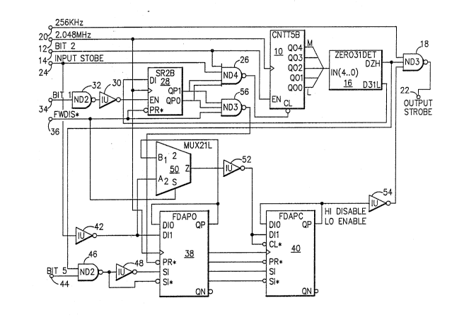
DESCRIPTION OF THE DR~WING
The drawing provides a schematic diagram of the
present invention.
DETAILED DESCRIPTION OF THE PREFERRED EMBODIMENT
Referring to the figure, there is shown a
schematic diagram for a flywheel circuit. The circuit
is particularly adapted for a system having frames with
a duration of 125 us, each frame having 32 time slots
numbered from 0-31, with each time slot including eight
bits of data. The time slots have a frequency of 256
KHz, while the bit rate is 2.048 MHz. It is to be
understood that these parameters illustrate only one
environment in which the present invention may function
and by no means restrict the scope of the invention.
.~ ~
-6-
9 3 ~
. .
The flywheel circuit is centered around a five-bit
counter lo which receives a 2.048 MHz clock signal from
a terminal 12. The enable input of the counter 10 is -
connected to a terminal 14 which receives a strobe
signal upon the occurrence of a second bit of each time -~
slot. Thus, the counter is incremented during the
second bit of each time slot and repeatedly counts from
0 to 31, providing five parallel outputs to a detector .. ~ :
16, which includes logic to provide a DZH output at a 1 :
,. . ~
level when the counter output is zero, and provides a
D31L output at the 0 level when the counter output is
31. The DZH output is connected to an input of a NAND
gate 18, which also receives an input from a terminal
20 which is connected to a 256 KHz clock signal. The `~:
256 KHz clock has a one-eighth duty cycle and goes high ; :~
or to the 1 level only during the last bit of a time
~:'v;. ~
slot or during bit time 8. The output of NAND gate 18 -~
is connected to a terminal 22 which provides the output -:~
strobe at bit tlme 8. ~ .
When the counter is running, an output strobe is ~ :
provided in each frame during the time slot in which
the counter output goes to zero.
The counter may be synchronized to the time
slot of an input strobe received at a terminal 24. The
input strobe is generated by an associated system
-7~
~ . ,:
~6 ~.. ,,"~"~ ,".~ ,",.". "" ~",' ~
2~13~3~
during a time slot in accordance with the assignment
data inputted to the system. I~erminal 24 is connected
to an input of a NAND gate 26 which has another input
connected to terminal 14 for receiving the bit time 2
strobe. NAND gate 26 has an output connected to a
clear input of counter 10.
A two-bit shift register 28 functions as a strobe
timing comparator and in conjunction with gate 26 as a
clock re-synchronizer. Register 28 has a data input,
DI, connected to the D31L output of detector 16. A
clock input is connected to terminal 12 for receiving
the 2.048 MHz clock. An enable input, EN, of register
28 is connected to an output of an inverter 30 which
has an input connected to an output of a NAND gate 32.
Gate 32 has one input connected to terminal 24 for
receiving the input strobe, and a second input .
connected to a terminal 34 which receives a strobe
during the first bit of each time slot. Register 28
also has a preset input, PR*, connected to a terminal
36 which receives a flywheel disable signal, FWDIS*.
Register 28 also has two outputs QP0 and QPl. ~
During bit time 1 of a time slot in which there is ~ :
an input strobe, register 28 is enabled. If the
counter 10 is in sync with the time slot of the input
strobe, the counter will, during bit time 1 of the time
-8-
2~3193~
slot, still be outputting a count of 31, since it is
incremented at bit time 2. Thus, during bit time 1, a
O-level signal is provided to the data input, DI, of ~ ;
register 28, resulting in a O-level signal at output
QPO of the register. If the input strobe appears in a
i, ..
time slot other than the one to which the counter is
synchronized, the output from detector 16 on DL31L will
not be O when register 28 is enabled, and the register
will be incremented to provide a 1-level output at
QPo. If a second input strobe arrives in a time slot ~ -
out of sync with the counter, the shift register will `~ -
again be incremented to provide two 1-level outputs at
QPO and QPl.
Outputs QPO and QP1 of register 28 are also ~`
connected to inputs of NAND gate 26. Thus, when both
outputs of register 28 are incremented to 1-level
signals during bit time 1, NAND gate 26 will see during
bit time 2 all l-level inputs and the counter will be
.~,
cleared to provide a O output, thereby synchronizing `
the counter to the time slot in which the input strobe
was received. `~
If an input strobe on terminal 24 appears in a
time slot that is not in sync with counter lO, register
28 will register a 1-level signal at output QPO, as
mentioned previously. However, if the next input ; `
_9_ ~:`. ,,'.1`
2~3~93~
strobe arrives in a time slot that is in sync with
count~r lo, a O-level will be received on the data
input of the register so that the outputs from the
register will be O and 1, which will not result in a
clearing or a re-synchronization of the counter 10, and
the out-of-sync input strobe will essentially be
ignored. Thus, the flywheel circuit continues to
provide output strobes in the same time slot of each
frame, if only one input strobe is missing from the
assigned time slot of a frame.
The flywheel disable FWDIS* signal is O when the
flywheel is to be disabled. The presence of a O input
on the preset input of register 28 causes both outputs
of the register to go a 1 level, which results in the
counter being cleared during bit time 2 of the next
time slot in which an input strobe is received, thereby
setting the counter to zero, which will initiate the
generation of an output strobe on terminal 22. As long
as the flywheel disable signal is 0, the counter will
be reset every time slot when an input strobe appears
on terminal 24, and an output strobe will be generated
on terminal 22. Thus, the flywheel is disabled, and an
output strobe is generated for each input strobe.
-10-
~ ~'
: : ,:.
2~31934
If the input strobe on terminal 24 ceases to
occur, the register 28 will not be enabled, and the
flywheel circuit will continue to generate output
signals in the assigned time slot of each frame. Thus,
provisions must be made to disable the output if the
input strobe ceases for two or more frames. To provide
this capability, two 2-input D-type flip-flops 38 and -~
40 are provided. Flip-flop 38 receives at an input DIl
the input strobe through an inverter 42. Select inputs
SI and SI* are provided with inputs sensitive to a DZH
signal from detector 16, and to a bit time 5 strobe
appearing on a terminal 44. A NAND gate 46 rece~ves
the DZH signal and the bit time 5 strobe so that the ;~ ~
DZH signal is sensed after the counter 10 has been -
incremented at bit time 2. An output of gate 46 is
connected to an input of an inverter 48, with an output ~
of inverter 48 being connected to the SI input of flip- -
flop 38 and the output of gate 46 being connected to
the SI* input of flip-flop 38. Thus, during bit time 5
when the counter is at zero, the input strobe will be ;
entered into the flip-flop at DIl as a O-level signal.
When bit time 5 ends, the selected input of the flip-
flop 38 switches to DIO, since the signals at the
select inputs will reverse after bit time 5. The DIO
input of flip-flop 38 is connected to the QP output,
--1 1--
2~3:L~33~
thus maintaining the output of flip-flop 38 at a O
level. If the input strobe is not present during bit
time 5 in a time slot when the DZH signal is 1, a 1-
level signal will be entered into the DI1 input of flip-
flop 38, generating a l-level signal at the output QP,
which will be maintained after the signals to the
select inputs reverse polarity at the termination of
the bit time 5 strobe, or when the DZH signal goes to
0.
The output QP of flip-flop 38 is connected to an
input of a multiplexer 50, which input would normally
be fed to a multiplexer output and to an inverter 52,
an output of which is connected to the DIl and clear
inputs of flip-flop 40. Inverter 52 is necessary,
since the output of the multiplexer 50 is inverted. If
the output of flip-flop 38 is 0, this will appear as O
at the DI1 and clear inputs of flip-flop 40, resulting~:~
in O-level signals at an output QP of flip-flop 40,
since the presence of a O at the clear input
immediately clears the flip-flop and puts a O on output:~
QP. The input select inputs of flip-flop 40 are
connected to the input select inputs of flip-flop 38;
therefore, the inputs will switch simultaneously with
the inputs of flip-flop 38, and the O-level signal at
-12-
','`~' ''~'''"''
; , .....
. .,~
','~'.''.~ '.
2~3:~934
,.
" .
the output will be maintained as it is ~ed back to the
DIo input.
The QP output of flip-flop 40 is connected to an
inverter 54, the output of which is connected as a
third input to NAND gate 18. A l-level at the QP
output of flip-flop 40 will result in disabling the
output on terminal 22, while a low signal on output QP :~
of flip-flop 40 will enable the output.
If an input strobe is missing when DZH of detector
16 is at a 1 level, and during bit time 5, and flip-
flop 38 is set to the 1 state, this appears at the DI1
input of flip-flop 40 and would be ready to be clocked
in at the next frame, when the flip-flop input is ` `~:
switched from DIO to DIl during bit time 5, when DZH is
at a 1 level. If, in the next frame, the input strobe
is still missing, the output of flip-flop 38 will
remain 1, and the output of flip~flop 40 will change to
a 1-level, resulting in the disabling of output 22. If :~
perchance the input strobe returned to its proper time
slot, flip-flop 38 would receive a O-level input and
provide a O-level output, while flip-flop 40 would ;~
clock in a 1-level signal during bit time 5. However, ~ .
immediately thereafter the clear input of flip-flop 40
would receive the O-level output from flip-flop 38, so
that by bit time 7, flip-flip 40 would be cleared to
-13-
2~3~93~
provide a O-level output, thereby enabling the output
strobe at terminal 22. Thus, flip-flops 38 and 40
function to disable the output if the input strobe is
missing for two consecutive frames or more.
A select input of multiplexer 50 is connected to
the flywheel disable signal, FWDIS*, at terminal 36, so
that when the flywheel disable signal is O the
multiplexer 50 receives its input from the output of
inverter 42, to essentially bypass flip-flop 38. Flip-
flop 40 will continue to function and provide an output
level 1, if the input strobe does not occur when DZH is
at a 1 level during bit time 5, to thereby disable the
output. Thus, a FWDIS* O-level signal disables the
flywheel so that an output strobe is produced for each
input strobe. However, flip~flop 40 functions to
disable the output strobe if there is no input strobe.
This could happen by the cycling of counter 10 back to
zero as a result of its normal counting, and not as a
result of clearing by an input strobe.
A NAND gate 56 is connected to receive the two -~
outputs of register 28 and the flywheel disable signal,
to provide a O-level output only when the flywheel is `
not being disabled and when the counter is being re-
synchronized as the result of the presence of two 1-
level signals at the outputs of register 28. The --~
-14- -
,: ,.. .
;. ~.::- ..
:, ,, ., .,: .;,:
.... ...
,.. - . :, -~: .
. .; . .
2a3ls3~
output of NAND gate 56 is connected to the preset
inputs of both flip-flops 38 and 40 to effectively
drive the outputs to a l-level when NAND gate 56 goes
to a O level. Thus, when the flywheel disable signal
is at a 1 level, indicating that the flywheel is not
disabled, and shift register 28 indicates that the
counter 10 should be re-synchronized, NAND gate 56
functions to cause the output to be disabled until the
counter is properly synchronized with the input strobe
which can result when the input strobe appears in the
same time slot for two consecutive frames. During a
first frame, re-synchronization is attempted during bit
time 2, during the second frame there should be ~ ~
synchronization, and register 28 should enter a O-level --;
input at bit time 1. Gate 56 will then no longer see
all ls, and the disable signal will be removed.
Thus, the output of NAND gate 18, which is the
output of the flywheel circuit, is synchronized to the
time slot of an input strobe received on terminal 24,
so that the output and input strobes both occur in one ;~
assigned time slot of each frame. If the input strobe
stops for one frame, the flywheel circuit will continue
to provide an output strobe on terminal 22; however, if
the input strobe stops for two frames, the output
strobe will ba disabled because both flip-flops 38 and
-15~
3 ~
40 will register a 1-level signal. If the input strobe
occurs in a time slot that is not in sync with the
counter, the shift register 28 will provide a 1-level
output on a single output terminal. If the time slot
of a second input strobe is in sync with counter 10,
the shift register 28 still provides a 1 and a O
output, and nothing happens; however, if a second input
strobe occurs in a time slot out of sync with counter
10, shift register 28 provides two 1-level outputs, and
the counter is cleared and re-synchronization is
attempted. In the meantime, the presence of two 1-
level signals at the outputs of shift register 28 cause
NAND gate 56 to provide a O-level signal and flip-flops
38 and 40 to provide l-level outputs, thereby disabling
the flywheel circuit output. However, if in the next
frame the counter is properly synchronized with the
time slot of the input strobe, a O-level signal will be
entered into shift register 28, which will cause output
QPo to go to o, thereby removing the O-level at the
preset inputs of flip-flops 38 and 40, and allowing the
flip-flops to go to a O-level at the next simultaneous ~
occurrence of a 1-level on the DZH output of detector ~`
16, a bit time 5 strobe and an input strobe. Thus, the ~ -
input strobe must be in the same time slot for two ;-
: ~. . . ,-
-16- -
,, ,., ,. "., ~.
: ' ' '
'~ '.'''"'.'"
, .,.,:
...`,' ;~'-''
:' ': '-~.':
2~3193~
frames before the counter is fully synchronized and
signals are provided at output terminal 22.
Thus, the present invention satisfies all of the
objectives set forth in the Summary of the Invention
and provides a flywheel circuit that will reduce the
chance of errors occurring in input data or input
strobes from producing output signals or output strobes
in an incorrect time slot.
The counter described in the present invention was
selected to be a five-bit counter to correspond to a
frame having 32 time slots; however, it is to be
understood that any other frame length could be used ~-
with an appropriate-sized counter. A two-bit register
was used to require the input strobe to be in an
incorrect time slot for two frames before re-
synchronization is initiated; however, a greater number
of frames could be selected by merely using a shift
register having a greater length. Two flip-flops were
used to detect the absence of input strobes for two
frames before the output is disabled. A greater number~ :
of flip-flops could be used to further delay the
disable function.
Thus, the present invention uses the concept of
inertia by employing a flywheel circuit to delay
reaction to a changed input.
-17-