Note: Descriptions are shown in the official language in which they were submitted.
2p320~~
i1743gil.abr I-520 21.11.1990
FIELD OF THE INVENTION
The present invention relates to civilian satellite
communications and more particularly to satellite communications
systems and techniques useful in financial transactions.
BACKGROUND OF THE INVENTION
With the significant increase in the use of consumer
credit and other financial facilities, the need for quick,
reliable and low-cost verification of creditworthiness has gained
in importance. Currently credit verification facilities are based
on land-based telephone Iines and involve a cost of approximately
ten cents per transaction.
1
~~~0~~
SUMMARY OF THE INVENTION
The present invention seeks to provide a low cost,
quick, reliable two-way point to multipoint satellite
communications system which is particularly suitable for handling
intermittent high density bursts of communications.
There is thus provided in accordance with a preferred
embodiment of the present invention a satellite communication
system comprising a central satellite communication terminal and
a multiplicity of remote satellite communication terminals which
communicate via a satellite, apparatus associated with each of
the multiplicity of remote satellite communication terminals for
transmitting a burst of information within a time slot and having
a characteristic which is independent of the time slot and
receiving apparatus associated with the central satellite
communication terminal for acquiring the characteristic during
each time slot and receiving the burst according to the time slot
and according to the characteristic, whereby multiple
transmissions may occur concurrently within a given frequency
bandwidth.
According to a preferred embodiment of the present
invention, the characteristic is also independent of time
synchronization with the central satellite communication
term:Lnal.
Add:Lt3onally in accordance with a preferred embodiment
of the invention, the characteristic is a frequency
characteristic.
Alternatively according to another preferred embodiment
2
of the invention, the characteristic is a phase characteristic
indicating the position of transmission windows within a given
time slot. In this embodiment, matched Chirp filters may be
advantageously employed in both the central and remote satellite
communications terminals to enable transmission to be effected
within a generally constant amplitude envelope, which is
particularly suitable far satellite transmissions.
In accordance with the present invention the remote
satellite communications terminals may employ relatively
frequency unstable oscillators, significantly lowering the cast
thereof without degradation. of performance.
There is also provided in accordance with a preferred
embodiment of the present invention a satellite communication
system comprising a central satellite communication terminal and
a multiplicity of remote satellite communication terminals which
communicate via a satellite; apparatus associated with the
central satellite communication terminal for transmitting
information having a wide band modulation characteristic and
apparatus associated with the remote satellite communications
terminals For receiving the information according to the wide
band modulation characteristic, the apparatus for transmitting
and the apparatus for receiving employing matched Chirp filters
to enable transmission to be effected within a generally constant
amplitude envelope, which is particularly suitable for satellite
transmissions.
Additionally in accordance with a preferred embodiment
of the invention each of the multiplicity of remote satellite
communication terminals which is operative for receiving includes
3
an antenna whose size is sufficiently small tlxat in the absence
of the use of linear FM Chirp waveforms or spread spectrum
processing in transmission, the satellite power spectral density
would exceed 6 db6~/4Khz in the Ku band.
Where is thus grovided in accordance with an embodiment
of the presewt invention a satellite communication system
including a plurality of remote satellite communication terminals
which communicate via a satellite and apparatus associated with
each of the plurality of remote satellite communication terminals
for transmitting and receiving information and including
apparatus for transmitting and receiving linear FM Chirp
waveforms carrying the information.
Preferably each of the plurality of remote satellite
communication terminals which is operative for transmission
includes an antenna whose size is sufficiently small that in the
absence of the use of linear FM Chirp waveforms or spread
spectrum processing in transmission, the off-beam power spectral
density emitted from the transmitting antenna would exceed 15 -
,251og(theta) dbW/4Khz for theta between 1 and ~ degrees for the
Ku band.
For the purposes of the present application, spread
spectrum processing is defined to mean a process wherein a
modulated communication signal is multiplied by a relatively high
rate periodic digital sequence of phases, thereby causing rapid
phase shifts of the original signal, and providing a widened
frequency bandwidth and a consequently lowered power spectral
density.
CE
Additionally in accordance with a preferred embodiment
of the present invention, each of the plurality of remote
satellite communication terminals which is operative for
receiving includes an antenna whose size is sufficiently small
that in the absence of the use of linear FM Ghirp waveforms or
spread spectrum processing in transmission, the satellite power
spectral density would exceed 6 dbW/4Khz in the Ku band.
~o~~oz~
BRIEF DESCRIPTION OF THE DRA6JINGS
The present invention will be understood more fully from
the following detailed description, taken in conjunction with the
drawings in which:
Fig. 1 is a generalized block diagram illustration of a
satellite communications system constructed and operative in
accordance with a preferred embodiment of the present invention;.
Fig. 2 is a generalized block diagram of a remote
satellite communications terminal useful in the system of Fig. 1;
Fig. 3 is a generalized block diagram of a central
satellite communications terminal useful in the system of Fig. 1;
Fig. 4 is a generalized block diagram of part of the
circuitry of the terminal of Fig. 2;
Fig. 5A is a generalized block diagram of another part
of the circuitry of the terminal of Fig. 2 constructed and
operative in accordance with one embodiment of the invention;
Fig. ~B is a generalized block diagram of another part
of the circuitry of the terminal of Fig. 2 constructed and
operative in accordance with another embodiment of the invention;
Fig. 6A is a generalized block diagram of yet another
part of the circuitry of the terminal of Fig. 2 constructed and
operative in accordance with one embodiment of the invention;
Fig. 6B is a generalized block diagram of yet another
part of the circuitry of the terminal of Fig. 2 constructed and
operative in accordance with another embodiment of the invention;
Fig. '7A is a generalized block diagram of part of the
circuitry of the terminal of Fig. 3 constructed and operative in
s
accordance with one embodiment of the invention;
Fig. 7B is a generalized block diagram of part of the
circuitry of the terminal of Fig. 3 constructed and operative in
accordance with another embodiment of the invention;
Fig. 8 is a generalized block diagram of still another
part of the circuitry of the terminal of Fig. 3;
Fig. 9 is a generalized block diagram of yet another
part of the circuitry of the terminal of Fig. 3;
Fig. 10 is a generalized block diagram of part of the
circuitry of Figs. 5A and 5B;
Fig. 11 is a generalized block diagram of another part
of the circuitry of Fig. 5A;
Fig. 12 is a generalized block diagram of another part
of the circuitry of Fig. 5B;
Fig. 13A is a generalized block diagram of part of the
circuitry of Fig. 8 constructed and operative in accordance with
one embodiment of the invention;
Fig. 13B is a generalized block diagram of p art of the
circuitry of Fig. 8 constructed and operative in accordance with
another embodiment of the invention;
Fig. 14 illustrates (not to scale) a plurality of time
slots;
Fig. 15 illustrates in enlargement but also mot to
scale, a portion of a time slot including a multiplicity of
transmiss~.on windows;
Fig. 16 illustrates that multiple users may transmit
within the same time slot without interference therebetween;
7
~o~~~~~
Fig. 1'7 illustrates conversion of the pulsed RF
transmission of Fig. 15 to a constant envelope amplitude
transmission through the use of a Chirp filter;
Fig. 18 illustrates the signal which results from
passing the modulated signal of Fig. 17 through a matched filter
and envelope detector;
Fig. 19 shows the frequency spectrum of the Chirp
modulated transmitted signal;
Fig. 20 illustrates the frequency spectrum of a single
DPSK modulated transmitted signal within the same frequency
bandwidth as in Fig. 19;
Fig. 21 illustrates the presence of multiple DPSK
modulated transmitted signals within the same frequency bandwidth
as in Figs. 19 and 2C?; and
Fig. 22 illustrates the transmitted signal of Fig. 20 in
the time domain.
8
~~~2~2~
DETAILED DESCRTPTION OF PREFERRED EMBODIMENTS
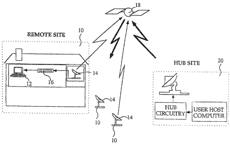
Reference is now made to Fig. 1, which illustrates a
satellite communications system constructed and operative in
accordance with a preferred embodiment of the present invention
and which is particularly suitable for transmission of bursts of
information containing data concerning individual financial
transactions.
In accordance with a preferred embodiment of the
invention, there are provided a multiplicity of remote satellite
communications stations 10, each of which may be coupled to a
corresponding user interface 12, such as a credit verification
unit of the type commercially used in retail outlets, or
alternatively, an IBM PC computer, which may be located at a
retail. outlet, for example. Each of the remote satellite
communications stations 10 typically comprises a very small
aperture antenna 14, typically of diameter of less than about
four feet and a communications terminal 16.
According to a preferred embodiment of the invention,
the communications terminal 16 comprises apparatus for
transmitting a burst of information within a time slot and having
a characteristic which is independent of the time slot and which
does not require pre-synchronization with a receiving terminal.
Each of the multiplicity of remote stations 10
communicates via a satellite 18 with a central communication
station 20 (Hub Site), which may, for example, be coupled to a
bank's or credit card company's central credit verification
computer via a conventional interface (riot shown).
9
~~~~~~8
Preferably the mode of communication from the remote
stations 10 to the central communication station 20 is full
duplex wherein bursts of information are sent by the remote
stations 10 on a random access basis , such as slotted Aloha, to
the central communication station 20. It is a particular feature
of the present invention that a very large number of remote
stations 10 can communicate with the central communication
station 20 on a random access basis without unacceptable
interference. Such interference would normally arise due to the
fact that a plurality of remote stations 10 may transmit within
the same time slot over the same frequency band.
According to the present invention, such interference
is greatly reduced by allowing each remote station to select an
additional recognizable transmission characteristic, such as the
center frequency of the carrier, or alternatively the phase of
the transmission windows within a time slot. The central station
is able to recognize this additional characteristic by simple
searching and without requiring synchronization. By recognizing
the additional characteg~istic, the central station effectively
distinguishes between multiple transmissions arriving within the
same time slot, thus creating additional effective channels for
receiving transmissions.
Reference is now made to Fig. 2, which illustrates, in
generalized block diagram form, a remote satellite communications
terminal useful in the system of Fig. 1. The remote satellite
communications terminal is coupled to antenna 14 via an ortho
mode polarizer 28, such as model 1810801 manufactured by Antennas
2~~2Q28
For Communications Inc, of Ocala, Florida, U.S.A. and typically
includes a low noise block (LNB) converter 30, such as, far
example, a Phase Lock Loop Low Noise Block Converter NHZ-170
manufactured by Japan Radio Company of Tokyo, Japan, or
alternatively an Ordinary Low Noise Block Converter NOR-640.,
commercially available from Norsat of Canada. Converter 30 deals'
with received signals from the antenna 14.
Signals to be transmitted via the antenna 14 are
supplied via polarizer 28 by a DRO-based Up-Converter 32, which
will be described hereinbelow in greater detail with reference to
Fig. 4.
Received signals from LNB converter 30 are supplied to a
demodulator 34, which will be described hereinbelow in greater
detail with reference to Figs. 6A and 68. The output of
demodulator 34 is supplied to network control logic circuitry 36,
which is typically based on an Intel SBC 188/56 chip.
The network control logic circuitry interfaces with a
User Processor 38, such as an IBM PC computer. Data and control
signals to be transmitted are supplied from the network control
logic circuitry 36 to a modulator 40, which is described
hereinbelow in greater detail with reference to Figs. 5A and 5B.
Modulator 40, in response to the control signals, transmits the
data to the converter 32.
Network control logic circuitry 36 performs two
principal functions:
Firstly, it initiates transmission of data to the
central satellite communication terminal, awaits an acknowledge
11
signs l therefrom and in the absence of such an acknowledge
signal, retransmits the data in a later time slot. It may
pseudorandomly or deterministically select an appropriate later
time slat for transmission.
Secondly, it randomly or pseudorandomly selects an
additional recognizable transmission characteristic, such as the
center frequency of the carrier, or alternatively the phase of
the transmission windows within a time slot.
Reference is now made to Figs. 3 and 9, which
illustrate, in generalized block diagram form, a central
satellite communication terminal 20 useful in the system of Fig.
1. Received signals from an antenna 50, such as a 6.1 KPK
manufactured by Vertex of Kilgore, Texas, U.S.A., are supplied
via a low noise amplifier 52 (not shown in Fag. 3}, such as a NC4
manufactured by LNR Communications, Inc. of Hauppauge, New York,
U.S.A, to a down converter 54, Such as a DC 4020 manufactured by
Satellite Transmission Systems, Tnc. of Hauppauge New York,
U.S.A.
Signals to be transmitted are supplied via an up
converter 56, such as a DC 6Q20 manufactured by Satellite
Transmission Systems, Tnc., to a high power amplifier (HPA) 58,
which is aommercially~available from Varian of the U.S.A, to
antenna 50. The up converter 56 receives an input from a
modulator 60 which will be described in greater detail
hereinbelow with respect to Fags. ~A and 7B.
Network Control Processor and Acknowledge Logic
circuitry 62 controls operation of the modulator 60 and of a
plurality of receivers 64 and receives data from the plurality of
12
receivex~s 64. Circuitry 62 is responsible for transmission of
instructions and data from a host computer 66 to the modulator
and from the receivers 64 to the host computer 66. Generally
speaking, the function of circuitry 62 is to recognize incoming
data bursts received from remote satellite communication
terminals 10 (Fig. I) and to provide acknowledge messages for
transmission to the remote terminals IO in response to the
received 'bursts.
The circuitry 62 and receivers 64 will be described in
greater detail hereinbelow with reference to Fig. 8.
Reference is now made to Fig. 4, which illustrates the
structure of the DRO-Based Up-Converter circuitry 32 (Fig. 2), An
L-Band signal, in the frequency range of about 950 - 1450 MHz is
supplied to a series of L-Band amplifiers 70,. such as MAR2
amplifiers, manufactured by Mini Circuits of Brooklyn, New York.
The output of amplifiers 70 is supplied via a low pass filter 72
of conventional construction to a mixer 74, such as a Ku-Band
Mixer, for example, a MC-5807 available from NEC of Japan.
A dielectric resonator oscillator (DRO) 76, such as an
MC 580$ available from NEC of Japan, also supplies an input to
the mixer 74, producing,a Ku-Band output which is supplied via a
series of Ku-Band amplifiers 789 typically including MC-5864 and
MC-5865 amplifiers available from NEC of Japan. The amplified
output of amplifiers 78 is supplied to polarizer 28 (Fig, I).
Reference is now made to Fig. 5A, which illustrates one
preferred embodiment of modulator 40 (Fig. 2). The modulator of
Fig. 5A incorporates a DPSK modulator 80, which will be described
i3
~~~~2~
hereinbelow in greater detail with reference to Fig. 11. The
output of modulator 80 is up converted to L-Band, in the range of
about 950 - 1450 MHz, by a mixer 82, such as a ZFM-2000 available
from Mini Circuits and a synthesizer 84, which operates at a
selected frequency in the range of about 1429.5 - 1929.5 MHZ in
response to frequency control signals received from network logic
circuitry 36. Synthesizer 84 will be described in greater detail
hereinbelow with reference to Fig. 10.
Reference is now made to Fig. 5B, which illustrates
another preferred embodiment of modulator 40 (Fig. 2). The
modulator of Fig. 5B incorporates a Chirp generator 90, which
will be described hereinbelow in greater detail with reference to
Fig. 12. The output of generator 90 is up converted to L-Band, in
the range of about 950 - 1450 MHz, by a mixer 92, such as a ZFM-
2000 available from Mini Circuits and a synthesizer 94, which
operates at a selected frequency in the range of about 1429.5 -
1929.5 MHZ in response to frequency control signals received from
network logic circuitry 36. Synthesizer 9~1 may be identical to
synthesizer 84.
Reference is now made to Fig. 6A, which illustrates one
embodiment of a demodulator 34 (Fig. 2). The demodulator
illustrated in Fig. 6~A comprises a synthesized converter 100,
such as a TIF-9 available from Mitsumi of Japan, which receives
° an L-Band signal and converts it to a signal having typical
center frequency of 49.5 MHz. A second converter 102, such as a
STD-9 from Mitsumi converts the 4~9.5MHz signal to a 70 MHz
signal and supplies it to a PSIt receiver 104, such as an LM 46
available from M/A-Com/Linkabit of the U.S.A. The received data
14
output from PSK receiver 104 is supplied to network control logic
36.
Reference is now made to Fig. 6B, which illustrates
another embodiment of a demodulator 34 (Fig. 2). The demodulator
illustrated in Fig. 6B comprises a synthesized converter 110,
such as a TIF-9 available from Mitsumi of Japan, which receives
an L-Band signal and converts it to a signal having a typical
center frequency of 479.5 MHz. A second converter 112, such as a
STD°9 from Mitsumi; converts the 479-.SMHz signal to a 7~ MHz
signal and supplies it via an amplifier 114, such as a MAR-1
available from Mini Circuits, to a Chirp compressor 116
preferably of a linear FM type, commercially available from
Sawtek Inc. of the U.S.A.
The output of the Chirp compressor 116 is supplied via
an amplifier 118, such as an MAR -l available from Mini Circuits,
to an RF detector 120, such as a UTD°1000 available from Avantek
of the U.S.A.. The output of RF detector 120 is supplied to a
mixer 122, such as a SBL-l from Mini Circuits, which also
receives an input from a voltage controlled oscillator 124, such
as a M 83 of K & L Oscillator of 'the U.S.A.. Oscillator 124
receives a frequency control input from via a loop filter 126,
typically implemented as shown based on a 4741 operational
amplifier 128, available from Harris of the U.S.A. Circuitry
122, 124, 126 and 128 imple~ents synchronization of a plurality
of data transmission windows.
Loop filter 126 receives an input from the output of
mixer 122, whicri is also supplied to integrate and dump circuitry
130, which is also based on a Harris 4741 operational amplifier
chip. The output of circuitry 130 is supplied to an A/D converter
13 2, such as an AD 7820 from Analog Devices of the U.S.A., which
outputs to a Viterbi decoder 134, commercially available from
Comstream of San Diego, California, U.S.A.. An output from
oscillator 124 is supplied to elements 130, 132 and 134. The
output of decoder 134 is supplied to network control logic
circuitry 36 (Fig. 2).
Reference is now made to Fig. 10, which illustrates a
synthesizer forming part of the apparatus of Figs. 5A and SB. The
synthesizer comprises a voltage controlled oscillator 180,
preferably operating in the range of 1429.5 ~ 1929.5 MHz. An
example of such an oscillator is a VTO 8100, manufactured by
Avatek of the U.S.A. Oscillator 180 is locked to a selected
frequency determined by a frequency control input to a PLL
synthesizer 182, which is based on a TA 6359 chip available from
Toshiba.
Fig. 11 illustrates a DPSK modulator employed in the
circuitry of Fig. 5A. The modulator comprises a convolutional
encoder 190 commercially available from Comstream of San Diego,
California, which receives a remote data input. A temperature
compensated crystal .oscillator 192, such as a ZT-176,
manufactured by Greenray, Inc. of the U.S.A. provides a symbol
clock output to encoder 190 and also provides, via a divider 19~E,
such as a 74HC4040 of Motorola, a data clock output.
A flip flop 196 receives the output from encoder 190
and the symbol clock output of oscillator 192 and provides a
differential signal output to a mixer 200, such as a ZAD-1 of
16
Mini Circuits. The mixer receives an input from a frequency
source 1~8, which is available from RFM Monolithics Inc.,
typically at a frequency of 479.5 MHz and provides a DPSK signal
output.
Fig. 12 illustrates a Chirp generator forming part of
the circuitry of Fig. 5B. The Chirp generator comprises a
convolutional encoder 210 commercially available from Camstream
of San Diego, California, which receives a remote data input. A
temperature compensated crystal oscillator 212, such as a ZT-176,
manufactured by Greenray, Inc. of the U.S.A. provides ~ symbol
clock output to encoder 210 and also provides, via a divider 214,
such as a 74FIC4040 of Motorola, a data clock output.
The output of encoder 210 is supplied to a multiplexer
21$, which receives inputs from a pair of one shot circuits 215,
which receive the symbol clock output from oscillator 222. The
mult3.plexer 21$ outputs to a one shot circuit 2209 which outputs
to a mixer 221, such as a SBL 1 from Mini Circuits. The one shot
circuits may 'typically be embodied in Motorola MC74LS123 chips.
The circuitry described hereinabove including elements 216, 218
and 220 produces a digital PPM signal from the output of the
convolutional encoder 210.
Mixer 224 also receives a fixed frequency output from a
47.5 MHz RF source 222, which may be identical to frequency
source 198, thereby to provide a pulsed RF output to an expander
Chirp Device 226, available from SAWTEK, Inc. of Florida, U.S.A.
Details of the structure of the central communications
terminal 20 illustrated .in Fig. 3 will now be described with
17
2fl~2~~~
reference to Figs. 7A, 7B, 8, 13A and 138.
Referring now to Fig. 7A there is seen a PSK modulator,
forming part of the circuitry of Fig. 3. The modulator comprises
a convolutional encoder 140 commercially available from Comstream
of San Diego, California, which receives a remote data input. A
temperature compensated crystal oscillator 142, such as a ZT-176,
manufactured by Greenray, Inc. of the U.S.A> provides a symbol
clock output to'encoder 140 and also provides, via a divider 144,
such as a 74HC4040 of Motorola, a data clock output.
The output of encoder 140 provides an output to a mixer
146, such as a ZAD-l of Mini Circuits. The mixer receives an
input from a frequency source 148, which is available from RFM
Monolithics Inc.,, typically at a frequency of 70 MHz and provides
a PSK signal output.
Fig. 7B illustrates a Chirp modulator forming part of
the circuitry of Fig. 3. The Chirp modulator comprises a
convolutional encoder 150 commercially available from Comstream
of San Diego, California, which receives a remote data input. A
temperature compensated crystal oscillator 152, such as a ZT-176,
manufactured by Greenray, Inc. of the U.S.A. provides a symbol
clock output to encoder 150 and also provides, via a divider 154,
such as a 74HC4040 of~Motorola, a data clock output.
The output of encoder 150 is supplied to a multiplexer
158, which receives inputs from a pair of one shot circuits 156,
which receive the symbol clock output from oscillator 152. The
multiplexer 158 outputs to a one shot circuit 160, which outputs
to a mixer 164, such as a SBL 1 from Mini Circuits. The one shot
circuits may typically be embodied in Motorola MC74LS123 chips. ,
18
The circuitry described hereinabove including elements 156, 158,
and 160 produces a digital PPM signal from the output of the
convolutional encoder 150.
Mixer 164 also receives a fixed frequency output from a
70 MHz IF source 162, which may be identical to frequency source
198, thereby to provide a pulsed RF output to an expander Chirp
Device 166, available from SAWTEK, Inc. of Florida, U.S.A.
Reference is now made to Fig. 8, which illustrates
network control circuitry 62 and receivers 64 which form part of
the circuitry of Fig. 3. A plurality of receivers 170, which are
described hereinbelow in greater detail in connection with Figs.
13A and 13B, receive an IF signal typically at 70 MHz from the
down converter 54 (Fig. 3) and output data via a communication
controller 172 and a control bus 173 to a master CPU 174.
Communication controller 172 is typically a SBS 18$/56 board from
Intel and the master CPU may be a SBC 286j12 board from Intel.
The master CPU 174 includes logic circuitry for
providing acknowledge messages and is operative for interfacing "
with a FIost Computer (not shown) for data communication
therewith.
Reference is now made to Fig. 13A, which illustrates one
embodiment of a DPSK receiver useful in the invention. A 70 MHz
received signal is received via a band pass filter 230, typically
having a pass band of 70 plus/minus 5 MHz. The output of filter
230 is supplied to a pair of mixers 232, such as SBL-1 from Mini
Circuits. Each m3.xer 232 receives an input from a sine/cosine (0
- 90 degree) splitter 234, such as a PSCQ-2-90 by Mini Circuits.
19
~fl~2~~~
A voltage controlled oscillator 236 supplies a carrier
frequency to the splitter 234. The output frequency of oscillator
236 is determined by digital signal processing (DSP) circuitry
248 via a digital to analog converter 23$. Oscillator 236 is
typically a P-360-65 from Greenray Inc.; DSP circuitry 248 is
typically embodied in a MC56000 circuit from Motorola and the
digital to analog converter 23$ is typically a DAC 10 HT by
Burr-Brown.
The outputs of mixers 232 are respective in phase and
quadrature base band signals. Each of the mixer 232 outputs is
supplied via a low pass filter 240, which may be based on a
Harris 4741 chip, to an analog to digital converter 242, such as
an ADC 7820 from Analog Devices, which receives a timing input
from a voltage controlled crystal oscillator 244, such as an M83
from K & L.
The output voltage of oscillator 244 is determined by
the digital signal processing circuitry 248 via a digital to
analog converter 246; which may be identical to converter 238.
The outputs of analog to digital converters 242 are
supplied to DSP circuitry 248, which also interfaces with control
bus 173 (Fig. 8). The output of DSP circuitry 248 is supplied to
a Viterbl Decoder 250, commercially available :from Comstream,
which outputs received data via an RS 232 driver.
Reference is now made to Fig. 138, which illustrates a
Chirp receiver useful in the circuitry of Fig. 8. A 70 MHz
received signal is received via a band pass filter 260, typically
having a pass band of 70 plus/minus 5 MHz. The output of filter
260 is supplied, via an RF amplifier 262, such as a MAR-1 from
CA 02032028 2000-08-16
Mini Circuits, to a compressor Chirp device 264, commercially
available from SAWTEK. The pulsed RF output of device 264 is
supplied to an RF detector 266, such as a UTD-1000 by Avantek,
which outputs the envelope of the pulsed output via a flash analog
to digital converter 272, such as an AD9000 by Analog Devices, to
circuitry 273, forming part of each receiver, which searches for
the location of the pulse envelope within a timing window.
Circuitry 273 typically comprises a FIFO circuit 274,
such as an IDT 7203 by IDT, digital signal processing circuitry
276, which may be identical to DSP circuitry 248, a Viterbi
decoder 278 which may be identical to decoder 250 and an RS 232
driver 280, which may be identical to driver 252. A temperature
compensated crystal oscillator 268, such as a ZT-176 from Greenray
Inc. provides a timing output to the flash A/D circuitry 272 and
to circuitry 273 directly and via a ripple counter 270, such as an
MC74HC40404 of Motorola. The output of the ripple counter 270
provides a Chirp rate clock output.
Reference is now made to Figs. 14 - 19 which help to
illustrate the operation of the Chirp embodiment of the invention.
A basic reference to Chirp waveforms in communications
applications is "Principles of Modern Radar", Ed. J. L. Eaves and
E. K. Reedy, Van Nostrand Reinhold Company, NY, pp. 469-475.
Fig. 14 illustrates (not to scale) a plurality of time
slots 300, each having a typical duration of about 200
21
~~32~~8
milliseconds. Fig. 15 illustrates in enlargement but also not to
scale, a portion 302 of a time slot 300 including a multiplicity
of transmission windows 3011. Each window 304 has a typical
duration of 200 nanoseconds. The separation between transmission
windows 304 for a given user is typically 100 microsecond.
It is seen in Fig. 15 that pulsed RF energy may be
located in either the forward or the rearward pasition of each
time window 304. The position of the pulsed RF energy within the
window contains the binary data carried by the signal.
Reference is now made to Fig. 16, which illustrates that
multiple users may transmit within the same time slot without
interference therebetween.
Fig. 17 illustrates conversion of the pulsed RF
transmission of Fig. 15 to a constant envelope amplitude
transmission through the use of a Chirp filter. This conversion
is necessary because pulsed RF is not a suitable modulation
technique for digital communication via satellite due to its lack
of a constant envelope.
Fig. 18 illustrates the signal which results from
passing the modulated signal of Fig. 17 through a matched filter
and envelope detector. It is noted that the arrangement of the
informatian within the transmission window 304 in fig. 18 is
obtained by passing the signals of Fig. 15 through matched
filters and an envelope detector, as is conventional in pulsed RF
receivers. It is appreciated that passing the signals of Fig. 15
through a transmitter Chirp filter and through a receiver matched
Chirp filter does not change the arrangement of the result as
illustrated in Fig. 18.
22
Fig. 1g shows the frequency spectrum of the Chirp
modulated transmitted signal. A characteristic of the linear FM
Chirp signal is that its frequency spectrum, illustrated in Fig.
19, has a wide band characteristic relative to the transmitted
symbol rate of the modulated signal. As a result, the power
spectral density of the signal is significantly lower than that
of a conventional (BPSK, QPSK, FSK, for example) narrow band
modulated. signal.
The terms "Chirp" and '°linear FM Chirp" as used
throughout the present specification are intended to include
applications in which the FM of the Chirp is only roughly linear.
For the purposes of the present specification, a narrocv
b~.nd modulated signal is defined as a signal, 80,°d of whose power
occupies in the frequency domain less than four times its symbol
rate in Hertz. Symbols are defined as being the data, after
coding if any, which is used to modulate the carrier.
The transmitted power spectral density must be limited
in two practical cases:
Z. The power spectral density emitted from. a satellite
transponder is limited in order to prevent a situ ation where a
satellite terminal pointed to an adjacent satellite will receive
interference from the transponder. Here, for example, the FCC
limits the power spectral density emitted from Ku band satellites
for data applications to 6 dbW/4 Khz.
2. The off-beam pawer spectral density emitted from an
antenna which transmits to a satellite is limited in order to
prevent interference to an adjacent satellite. Here, for example,
23
the FCC limits the off-beam emission of an antenna transmitting
to a Ku band satellite to -14 +29 - 251og(theta) equals 15 -
251og(theta) dbW/ 4 Khz.
Reference is now made to Figs. 2C - 22 which help to
illustrate the Differential PSK embodiment of the invention. Fig,
20 illustrates the frequency spectrum of a single DPSK modulated
transmitted signal within the same frequency bandwith as in Fig.
19. Fig. 21 illustrates the presence of multiple DPSK modulated
transmitted signals within the same frequency bandwidth as in
Figs. 19 and 20. Fig. 22 illustrates the transmitted signal of
Fig. 20 in the time domain.
It will be appreciated by persons skilled in the art
that the present invention is not limited by what has been
particularly shown and described hereinabove. Rather the scape of
the present invention is defined only by the claims which follow:
24