Note: Descriptions are shown in the official language in which they were submitted.
2~3204~
PHA.21564 l 27-11-1990
Bilevel current limiter
This invention relates to a control circuit
for controlling and limiting via a semiconductor control
switch the start-up current supplied to a load in two or
more steps and in a manner so as to protect the semi-
5 conductor control switch from overload. More particularly,the present invention relates to a control circuit for
limiting the start-up current that flows through a semi-
conductor control switch connected in series circuit
with an incandescent lamp or similar load device whose
10 impedance exhibits a non-linear variation during the
turn-on phase thereof.
Due to the non-linear impedance characteristic
of an incandescent lamp or other similar non-linear
impedance load, a turn-on or inrush surge current occurs
15 which may be approximately ten times the steady state
or normal operating current of the lamp or other load.
If a semiconductor control device, such as a bipolar
transistor or a field effect transistor (FET), is connected
in series circuit with such a load across a pair of
20 voltage supply terminals, damage to the semiconductor
control device may occur at start-up unless some form
of surge current protection is provided.
For energizing a lamp, one known and common
constant current limiting technique is shown in Fig. 1
25 and includes a semiconductor power switch 1, such as an
FET, connected in series circuit with a small sensing
resistor 2 and the lamp 3 across a pair of voltage supply
terminals. The voltage developed across the sensing
resistor (Rs), which is proportional to the current
30 through the FET and the lamp, is applied to an input of
a comparator 4 having a fixed input offset voltage (VOS).
The output of the comparator is coupled via a logic
circuit 5 and a switch driver 6 to the gate or control
2032043
PHA.21564 2 27~ 1990
electrode of the series connected power switch (FET).
If the load current flowing through Fs is large enough
to trigger the comparator, a feedback signal is applied
to the gate or control electrode of the FET via the
logic circuit and the switch driver so as to turn-off
the power switch. Assuming the feedback delay is small
compared to the rise/faa time of the power switch (FET),
the load current will be limited to a constant value
(possibly with a small ripple component) equal to
Vos/Rs
Fig. lA depicts the relationship of load
current (IL) versus the output voltage (VO) across the
lamp for the lamp control circuit described above.
Also shown is the characteristic curve Tc for the tran-
sistor power switch which defines the safe operatingarea (SOA) for the series connected FET power switch.
The curve labelled TOC represents the turn-on charac-
teristic for the incandescent lamp and shows the
variation of the operation points during turn-on of the
lamp as it heats up and its filament rEsistance increases
continuously from a small resistance value Rc when it is
cold to a final steady state value Rh after it has
heated up.
In this type of prior art circuit, the current
is initially limited to a value IL1. If, during the time
that the power switch drives the lamp, part of the TOC
of the lamp remains outside of the SOA of the power
switch for a sufficient period of time, for example,
from the time instant t1 to the time instant t2, damage
to or destruction of the power switch may result due
to overload thereof.
There are three common methods for protecting
the power switch from overload during start-up of the
lamp. The first is to reduce the current limit value
from the value IL1 to a lower value IL2, where IL2 is
now the maximum current allowed to flow and its value
is chosen so that the current through the power switch
.
~ ,,
,
2032043
PHA.21564 3 27-11-1990
never exceeds its power capability over the entire
operating range of the load current and the load voltage.
A disadvantage of this technique is that the small
current flowing during start-up means less power is
delivered to the load (lamp) and so the lamp will heat up
and reach its normal operating resistance at a much
slower rate.
A second switch protection method is to use
a power switch with a much higher power handling capability
such that it can safely handle the maximum lamp current
which occurs when the filament is cold. This method has
the obvious disadvantage that it requires a much larger
power switch, a larger heat sink, etc; all of which
increases the cost and size of the circuit.
A third way of protecting the power switch is
to switch it on and off at a low duty cycle during the
initial time period when the lamp resistance is low
thereby to reduce the power dissipation in the switch.
One disadvantage of this approach is that the power
pulses generated produce undesirable electromagnetic
interference (EMI).
European Patent Application, EPA 0,285,417,
published October 5, 1988 discloses a solid state switch
for limiting the flow of start-up current to an incandescent
lamp. The control circuitry in this device initially
allows a relatively low constant current to flow through
the lamp and a series connected FET switch and then,
automatically, after the lamp resistance reaches a
preselected level, it is allowed to draw a significantly
higher current. The size and cost of the power FET is
reduced significantly because the magnitude of the
current spike generated at turn-on of the lamp is reduced.
A disadvantage of this circuit is that effectively it
provides only one current limit. When it switches over
automatically, a fairly large current spike nevertheless
is still allowed to flow, albeit lower than would
otherwise occur in the absence of the invention described
: .
: ' ' '
~03~
PHA.21564 4 27-11-1990
therein. Furthermore, that device uses operational
amplifiers to bias the current delivered to the lamp,
rather than comparators operative to clamp the current
to a certain value. As a result, the EPA apparatus
requires frequency compensation and is therefore harder
to implement in an integrated circuit.
The foregoing problems relates to the operation
of a lamp load are compounded in the case of an automotive
environment which requires special techniques to drive
an automotive lamp load.
It is therefore an object of the invention
to provide a control circuit for turning on and operating
an incandescent lamp or similar type Ioad by means of
a power transistor in which two separate current limits
are selected which track the SOA boundary of the
transistor characteristic thereby allowing a maximum
current to flow during turn-on of the lamp and without
exceeding the safe operating current limits of the
power transistor.
Another object of the invention is to provide
a two-level current limiting apparatus which monitors
the SOA of a power transistor and which allows an
incandescent lamp load or the like to turn on quickly,
reliably and without the generation of electromagnetic
interference or a current surge at the switchover point.
A further object of the invention is to provide
a bilevel current limiting control circuit for turning
on a load via a power transistor having a limited power
handling capability such that it maximizes the current
delivered to the load without exceeding the SOA limit
of the power transistor and without using pulses.
A still further object of the invention is to
provide a bilevel current limiting control circuit that
is especially useful for safely driving a lamp load in
an automobile.
The above and other objects are achieved by
means of an apparatus that includes a power transistor
- .
' ' : . .
2032~43
PHA.21564 5 27-11-1990
te.g. an FET), all or a part of which is connected in
serias circuit with a current sensing device (e.g. a
small resistor) and an incandescent lamp load or the
like across a pair of power supply terminals. First and
second comparators with first and second separate
trigger levels have their inputs coupled to the current
sensing device thereby providing two separate current
level limits. The outputs of the comparators are coupled
via a selector circuit to a control circuit whose output
is coupled via a switch driver to a gate or control
electrode of the power transistor to control the current
flow therein. A third comparator has an input coupled
to the load and an output coupled to a control input
of the selector circuit whereby either the output of
the first or second comparator is selected depending on
the level of the load voltage. This bilevel current
limiting feature enables a power transistor with a
limited power capability to operate near the inside
border of its SOA during turn-on of the lamp load thereby
2D providing rapid lamp turn-on without damage to the power
transistor and without the generation of electromagnetic
interference or current spikes.
The invention broadly operates to automatically
change the current delivered to an incandescent lamp
load or the like depending on the lamp (load) voltage
in a manner such that the power switch (transistor) is
protected from the initial current surge during turn-on.
The invention is based on the concept of monitoring the
safe operating area (SOA) of the power switch.
More particularly, by means of the invention, an active
current limit circuit supplies a current ~hat is
constrained to remain near, and preferably within, the
boundary of the SOA of the semiconductor power switch
so that an optimal level of current is delivered to the
load while simultaneously protecting the power switch
from excessive currents and thereby possible damage.
The invention provides two separate current limits
2~32~43
PHA.21564 6 27-11-1990
automatically selected to track the SOA boundary whereby
the maximum safe current is delivered to the lamp during
all phases of the turn-on operation. The invention thus
make it possible to safely deliver more current to the
power switch than prior art devices that do not use the
principle of monitoring the SOA of the power switch.
Another distinction between the invention and,
for example, the solid state switch described in EPA
0,285,417 A2 is that the EPA device uses operational
amplifiers to continuously bias the current supplied
to the load, whereas the invention uses comparators which
operate to clamp the current to a certain value.
This provides the advantage of ease of implementation
in certain high voltage processes, and also avoids the
requirements for frequency compensation in the op-amps,
a potential source of instability.
The invention will now be described in greater
detail in connection with the accompanying drawings in
which:
Fig. 1 is a block-schematic diagram of one
form of a conventional current limiter circuit for a
lamp load,
Fig. lA shows the relationship between load
current and load voltage for the current limiter clrcuit
of Fig. 1,
Fig. 2 shows a block-schematic diagram of a
preferred embodiment of the invention,
Fig. 3 shows the relationship between load
current and load voltage for the current limiter circuit
of Fig. 2 showing the SOA and the TOC, and
Fig. 4 is a circuit diagram of a selector
device for use in the apparatus of Fig. 2.
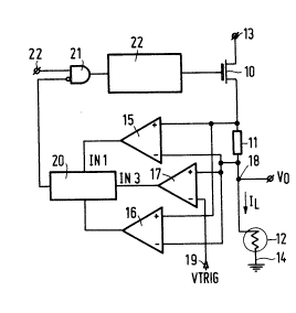
Fig. 2 shows a block-schematic diagram of a
preferred embodiment of the invention which comprises a
semiconductor power switch 10, for example, a field-
effect transistor (FET) connected in whole or in part
in series circuit with a sensing resistor 11 and a
load 12, for example, an incandescent lamp, across the
,~ , . ,~ .
~32~3
PHA.21564 7 27~ 1990
terminals 13, 14 of a source of DC supply voltage.
Terminal 14 may be connected to ground.
The resistor 11 senses the load current, IL,
and develops a voltage proportional thereto. The terminals
of the sensing resistor are coupled to the input terminals
of a first comparator 15 and to a second comparator 16
so that the voltage developed across the resistor, which
is proportional to the load current, is operative to
control the operation of the comparators. The comparators
15 and 16 have different levels of internal offset voltages
VOsl and VOs2 which operate as reference voltages to
determine the switching points of their respective
comparators and thereby set the first and second current
limits of the control circuit.
A third comparator 17 has one input (+)
connected to the load terminal 18 at which the load
voltage (VO) appears, and has a second input (-) connected
to an input terminal 19 which receives a reference
voltage, Vtrig. The output terminals of the first,
second and third comparators are connected to first,
second and third input terminals of a selector device
20, which may be a conventional multiplexor circuit,
one form of which is shown in Fig. 4. In Fig. 4, the
selector function is implemented using two bidirectional
CMOS switches and three inverters. The operation thereof
is well known and will therefore not be set forth in
further detail.
The output of the selector 20 is in turn
connected to one input of a logic circuit 21. A second
input of the logic circuit is connected to an input
terminal 22 which receives a signal for turning the
control circuit on. The output of gate circuit 21 is
connected to an input of a conventional switch driver
stage 22 having an output Connected to the gate or
control electrode of the power switch 10 in order to
control the conduction of the switch.
~ ' ' 1
-
2~320~
PHA.21564 8 27-11-1990
As shown in Fig. 3, when the current limiter
of Fig. 2 is first turned on, the resistance of the lamp
load 12 is initially low, i.e. it has a cold resistance
Rc, which establishes a first load line (Rc) for the
lamp element 12. After the current flows through the
load for a sufficient time period, the lamp heats up
so that the resistance thereof reaches its normal
operating value, Rh. This establishes the load line Rh
shown in Fig. 3. Between the initial (cold) and final
(hot) resistance values, the lamp resistance increases
so that a multiplicity of load lines (not shown) are
established. The load lines effectively rotate clockwise
from the resistance value Rc up to the resistance value Rh.
The third comparator 17 is responsive to the
load voltage VO~ which increases as the lamp heats up
and its resistance increases. The third comparator
operates via the selector device 20 to select the output
from either the first comparator 15 or the second
comparator 16 depending on whether the output voltage,
VO is greater or smaller than the reference voltage,
Vtrig, at the input terminal 19. The selected output
provides a feedback to the gate of the power switch
so as to control the state of the power switch 10.
When VO < Vtrig, the output of the comparator 15 is
selected, whereby the reference voltage, VOS1, of this
comparator sets the current limit for the series circuit
(10-12) to a low load current value IL2, as shown in
Fig. 3. Therefore, initially, the feedback circuit
operates to limit the load current flowing through the
power switch 10 to a value IL2 which lies within and
close to the boundary of the safe operating area (SOA)
for this transistor.
As the lamp resistance increases, a point X
on the lamp turn-on characteristic (T00) is reached
at which the output load voltage, VO' just exceeds the
value of the reference voltage Vtrig. At this point,
the third comparator and selector operate to select the
output of the second comparator 16 in place of the
2032~
P~A.21564 9 27-11-1990
output of the first comparator 15. The offset reference
voltage, VOs2, of the second comparator now sets the
current limit, via the feedback circuit coupled to the
gate of power FET 10, to a higher value, IL1 shown in
Fig. 3.
The lamp now heats up faster and its resistance
follows the portion of the TOC between points X and Y.
As can be seen in Fig. 3, the load current in the FET 10
closely follows the boundary of the SOA of the transistor
between points X and Y. Although the transistor current
slightly exceeds the SOA boundary between points X and
Y, it will not damage the transistor since the transition
period X-Y is very brief so that the transistor does
not have time to overheat.
Alternatively, the value of the reference
voltage Vtrig can be selected so that the point X
occurs at a later point in time (to the right in Fig. 3)
such that the TOC between points X and Y lies wholly
within the boundary of the SOA of the transistor.
The choice of Vtrig in Fig- 3 has the advantage that
the lamp heats up a little quicker, also without damage
to the power switch 10. By selecting a value of trigger
voltage such that Vtrig = (IL2/ L1)( DD o L1
where VDD is the supply voltage and PO is tha maximum
power limit of the switch 10, the TOC will remain within
the SOA boundary of the switch and at the same time
will provide close to the maximum available load current
at all times during the lamp turn-on phase. The result
is quick turn-on of the lamp, no damage to the power
switch, and no EMI generated.
The invention described has been implemented
and fabricated on a silicon chip as a special feature
of an intelligent power switch for use in automobiles.
Appropriate offset voltage were chosen to determine the
two current limits for the bilevel control circuit.
The circuit was tested for three different values of
load resistance. Current limiting was achieved by
'~3~Q~
PHA.21564 10 27-11-1990
turning the power switch on and off about a nominal
current. The on/off command was given by the output
of the selector switch.
The circuit waveforms were displayed on an
oscilloscope and showed the load voltage, V0, tracking
the increase in the value of the load resistance with
time. A slight discontinuity was observed in the load
voltage waveform at a load voltage of 8 volts, which
was the value chosen for Vtrig. This is the point in
time when the selector switched over from the first
comparator to the second comparator, changing the current
limit to a higher value (about 20% in the test).
This allowed more current to be delivered to the lamp
when the drain-to-source voltage of the power FET was
low. The corresponding waveform of the gate voltage of
the power FET showed a relatively small step increase
at the switchover point, Vtrig, and then increased
approximately linearly to a final constant value.
Controlled current limiting was achieved over the entire
rsnge of output voltage. The values of the current
limits and the transition voltage can be set, as
desired, by the user.
The foregoing description sets forth my
concept of a bilevel current limiting method and
apparatus for monitoring a semiconductor power device
by reference to the safe operating area of the power
device. Important advantages are that the control
circuit provides an active current limit which clamps
the current to first and second maximum values independent-
ly of the load, and there is practically speaking nocurrent spike generated at the transition from one
current limit value to the next.
The above description presents an exemplary
embodiment of the invention which is illustrative of
the spirit and scope thereof. Various modifications
can be made consistent with the principles of the
invention. The invention is not limited, for example,
.' .
2û~0~3
PHA.21564 11 27-11-1990
for use with an incandescent lamp load, but other
types of load consistent with the above description
come within the scope of the invention. It should
therefore be understood that the invention is to be
limited only by the scope of the accompanying claims.