Note: Descriptions are shown in the official language in which they were submitted.
~~~3O~
CIRCUIT AND METHOD FOR IIWiPROVED
DIMMING OF GAS DISCHARGE LAMgS
Backa~round of the Invention
Field of the Invention
This invention pertains to dimming gas discharge
lamps and, more particularly, to dimming fluorescent and
compact fluorescent lamps.
Description of the Related Art
A gas discharge lamp convervs electrical energy
l0 into visible energy with high efficiency. A gas discharge
lamp is generally an elongated gas-filled (usually low
pressure mercury vapor) tube having electrodes at each end.
Each electrode is formed from a resistive filament (usually
tungsten) coated with a thermionically emissive material,
such as a mixture of alkaline earth oxides.
The steady-state operation of a gas discharge lamp
is as follows: Voltage is applied across the resistive
filaments, heating the electrodes to a temperature suffi-
cient to cause thermionic emission of electrons into the
discharge tube. A voltage applied between the electrodes
accelerates the electrons toward the anode. En route to
the anode, the electrons collide with gas atoms to produce
positive ions and additional electrons, forming in the tube
a gas plasma of positive and negative charge carriers. The
electrons continue to stream toward the anode and the
6232-90.CN -1-
/lp/#11
~Q3~~~
positive ions toward the cathode, sustaining an electric
discharge in the tube and further heating the electrodes.
If the applied power is ac, the electrodes reverse polarity
on alternate half cycles.
The discharge causes the emission of radiation
having a wavelength dependent upon the particular fill gas
and the electrical parameters of the discharge. Because
each collision produces additional electrons and ions,
increases in the arc current can cause the voltage between
the lamp electrodes to decrease, a characteristic known as
"negative resistance." Operation of the lamp is inherently
unstable, due to this negative resistance characteristic,
and current between the electrodes must be limited by
external means to avoid damaging the lamp.
Gas discharge lamps, including fluorescent lamps,
are designed to deliver their full rated, or "nominal",
light output at a specified RMS lamp current value. In
this specification and the attached claims, the RMS current
value at which a lamp is designed to deliver its full rated
light output will be referred to as the "nominal°' value of
the lamp current.
Fluorescent gas discharge lamps include a phosphor
coating on the inside of the tubular housing, and the
excitation of this coating by radiation from the discharge
provides the visible light output. Conventional fluore-
scent lamps are generally straight elongated tubes of
essentially circular cross section with varying outside
diameters ranging between about one and one and one-half
inches.
Compact fluorescent Lamps differ form conventional
fluorescent lamps in that they are constructed of smaller
diameter tubing, having an outside diameter of less than
about seven-eighths of an inch. Also, the lamps are
compact in part because the tubing has multiple small
radius bends to fold back on itself in such a manner as to
achieve a compact shape.
6232-90.CN -2-
/lp/#11
CA 02032057 1999-04-20
Dimming of gas discharge lamps is well known. A
circuit for dimming a conventional fluorescent gas dis-
charge lamp is disclosed in U.S. Patent No. 3,927,345,
issued December 16, 1975, to Licata et al. Licata
discloses a phase control dimming circuit which provides
phase controlled voltage from a 60 Hz ac source to a
fluorescent lamp in series with an inductive ballast. The
dimming circuit employs a bi-directional triode-type
thyristor (triac) as the main switching device and includes
a do compensation circuit to ensure symmetrical triac
firing delays in each half cycle of power flow from ac
source. There is no current through the lamp during the
triac firing delay. Symmetrically firing the triac
prevents do current from flowing through the lamp, which
can cause the lamp to flicker and can cause saturation of
the inductive ballast. The circuit operates over a dimming
range from about 100% to 50% of full light output. Below
about 50% light output, the electric discharge cannot be
sustained, because the triac firing delay is longer than
the de-ionization time of the gas plasma in the discharge
tube.
Robertson Transformers Company of Chicago, Il-
linois, makes a lamp ballast of this type specifically
designed to operate compact fluorescent lamps. The ballast
has limited dimming range due to the aforementioned triac
firing delay and generally cannot dim below,40% of full
light output.
U.S. Patent No. 4,207,498, issued June 10, 1980, to
Spira et al., discloses a dimming system that includes a
central inverter for providing a substantially symmetrical
23kHz ac current through the lamp. The lamp can be dimmed
over a range form 100% to 1% of full light output by
adjusting the amplitude of the inverter output. The use of
high-frequency ac current also may increase the efficacy of
the lamp by as much as 20%. At low light levels (less than
about 30% of full light output), however, the lamp tends to
6232-90.CN -3-
/lp/#11
CA 02032057 1999-04-20
"striate"; i.e., to break up into alternating bands of
bright and dim areas along the length of the tube. This
limits the utility of this type of system for dimming over
a wide range of light output.
Previous attempts at dimming compact fluorescent
lamps have not been entirely successful. The best known
method is embodied in a product called HiLume~, manufac-
tured by Lutron Electronics Co., Inc. of Coopersburg, PA.
The operation of this product is described in U.S. Patent
No. 3,824,428, issued July 16, 1974, to Spira et al. and,
U.S. Patent No. 4,663,570, issued May 5, 1987, to Luchaco
et al. This product allows dimming of compact fluorescent
lamps to about 15% of their nominal light output. However,
below this light level, the lamps exhibit an annoying
flickering characteristic which makes them unsuitable for
illumination usage.
Another known dimming control for compact fluore-
scent lamps is manufactured by Innovative Industries of
Tampa, FL. This control can operate the lamps to light
levels below 15% without flicker, but suffers from poor
stability of lamp arc current when operated below about 40%
of nominal light output. The lamp arc current and there-
fore the light output of the lamp varies over a wide range
at a given setting of the dimmer. For example, when
operating a 26 watt quad tube T4 lamp, with an outside tube
3'i~meter of about one-half inch, this variation can be as ,
much as from 4.7 milliamperes to 13.9 milliamperes when the
lamp temperature varies over the range from normal room
temperature of about 25"C to its normal operating tempera-
ture of about 50°C. The wide variation of light output
which results from this range of arc currents is unaccep-
table in practical use. Specifically, if the lamp is
initially at room temperature when it is set to a desired
light level, the light at this setting could increase to as
much as about three time the initial light level when the
6232-90.CN -4-
/lp/#11
2~~zos7
lamp is warmed up to its normal operating temperature. If
the lamp is initially at some equilibrium operating temper-
ature and then is adjusted to a lower light level, subse-
quent cooling of the lamp causes the light level to drop
even lower, possibly even extinguishing the arc. This
makes it very difficult to obtain a desired light level as
required by the particular needs of the system user.
Summary of the Invention
The present invention provides a dimming control
which provides stable operation of compact fluorescent
lamps without flicker or striations over a range from about
100% to 1% of nominal light output.
One aspect of the present invention provides for
dimming of compact fluorescent lamps to below about 15% of
nominal light output without flicker by providing a sub
stantially symmetrical high frequency ac waveform to
operate the lamp. In a symmetrical ac waveform, the
duration, amplitude, and shape of the positive and negative
half cycles are substantially the same.
Another aspect of the present invention provides
for improved stability of light output at low light levels
when dimming compact fluorescent lamps below about 40% of
nominal light output by providing an unusually high output
impedance characteristic for the lamp current source. This
impedance is greater than about 5,000 ohms, and insures
stable operation of these compact fluorescent lamps, which
exhibit an unexpectedly high value of negative resistance
at low light levels compared to conventional fluorescent
lamps.
One embodiment of the present invention provides a
means of achieving this unusually high output impedance by
a combination of passive series impedance elements and
feedback control of the lamp arc current. This combination
allows the passive impedance elements to have a moderate
value of impedance, so that they are physically small and
6232-90.CN -5-
/lp/#11
2~x05?
have low energy loss, while the current feedback system has
a relatively low gain and improved stability, compared to
the use of either method alone.
In another embodiment of 'the present invention, the
dimming circuit generally provides a high-frequency current
to the electrodes of a fluorescent lamp to initiate and
maintain an electric discharge through the lamp and,
simultaneously, provide a small amount of do current to the
electrodes to produce a composite current waveform through
the lamp. The do current is small enough that it does not
produce adverse effects that are associated with operating
lamps on do and asymmetrical waveforms, but is sufficient
to significantly reduce visible striations in the lamp.
Alternatively, the do component can be replaced by a low
frequency ac component.
In another embodiment of the present invention, a
method for dimming fluorescent lamps consists of providing
to the lamp a composite current waveform including ac and
do current component. This composite waveform is par-
ticularly advantageous in compact fluorescent lamps when
the ac component of current is a substantially symmetrical
high-frequency waveform. The do component can be either
positive or negative and is preferably substantially
smaller in magnitude than the ac component. Alternatively,
the do component can be replaced by a low-frequency ac
component.
For purposes of this specification and the appended
claims, the term '°dc" refers to a voltage or current
waveform that is unidirectional and can be either pulsating
or non-pulsating. The term °'ac" refers to a voltage or
current waveform which reversed polarity at regularly
recurring intervals of time and has alternately positive
and negative values. The term "dc component" refers to the
average value of an ac or do waveform. The term "ac
component'° refers to that portion of an ac or do waveform
remaining after its do component has been subtracted.
6232-90.CN -6°
/lp/~11
z~zo~7
Brief Description of the Drawinas
Fig. 1 shows an asymmetrical waveform of a prior
art dimming system.
Fig. 2 is a voltage/current characteristic curve
for a typical fluorescent lamp.
Fig. 3 is a simplified circuit schematic of one
embodiment of the present invention.
Fig. 4 is another embodiment of the invention as
shown in Fig. 3.
Fig. 5 is a graph of current flow through a compact
fluorescent lamp according to the present invention.
Fig. 6 is a composite current waveform having high-
frequency and low-frequency ac components.
Fig. 7 is a simplified circuit schematic for
producing the waveform of Fig. 6.
Fig. 8 is a simplified circuit schematic for
providing pulsating, low-frequency do current to a lamp.
Fig. 9 is a simplified circuit schematic for
providing pulsating, low-frequency, asymmetric ac current
2U to a lamp.
Fig. 10 is a block diagram of a dimming circuit of
the present invention.
Fig. 11 is a circuit schematic of a dimming circuit
of the present invention.
Fig. 12 is a graph showing preferred characteris-
tics of a current sensing circuit of the present invention.
Detailed Description of the Present Invention
The resolution of the deficiencies of flicker,
unstable light output and striations in dimming systems for
compact fluorescent lamps is not obvious.
For example, the HiLume~ product described above,
is available for conventional fluorescent lamps having a
tubular shape and diameters down to about one inch. The
performance of these lamps extends to 1~ of nominal light
output with no flicker and good light output stability, so
6232-90.CN -~-
/lp/#11
the flicker observed below 15~ nominal light output when
this product is used to dim a compact fluorescent source is
quite unexpected.
Our investigation indicates that the flicker in
compact fluorescent sources is related to the presence of
anode oscillations in the lamp. Anode oscillations are a
well-known phenomena in gas discharge lamps which are
operated on dc, or on ac with a frequency which is slow
with respect to the de-ionization time of the lamp plasma.
However, it is generally understood that operating a lamp
at a high frequency eliminates anode oscillations. since
the HiLume~ product operates at such a high frequency,
approximately 27kHz, the presence of anode oscillations in
the compact fluorescent was unexpected.
The HiLume~ product provides a high-frequency ac
current to operate the lamp, but this current is not
symmetrical. Figure 1 is a diagram of the HiLume~ waveform
at low light output levels. Clearly, the waveform is not
symmetrical, as both the duration and the amplitude of the
positive and negative half cycles are quite different.
Note, however, that the area under the positive half cycle
is always equal to the area under the negative half cycle,
so that this is a pure ac waveform, with no do component.
The asymmetrical character of this waveform is advantageous
with conventional fluorescent lamps with a diameter of one
inch or more, as it gives very smooth dimming to light
levels of 1~ or less with no flicker or visible striations.
However, we have found that this asymmetrical waveform
induces anode oscillations in compact fluorescent lamps, in
spite of the high operating frequency of 27kHz, and this
causes the lamps to flicker below about 150 of nominal
light output.
According to our experiments, a difference in the
duration of the positive and negative half cycles of more
than 10~ of the duration of one full cycle will induce
anode oscillations and flicker in compact fluorescent
6232-90.CN -8-
/lp/#11
203245?
lamps. For example, if the lamp is operated with a rectan-
gular waveform having a total duration of 100~csee. for one
full cycle, then the positive half cycle (or the negative
half cycle) must have a duration between about 45 and
55~sec. to avoid anode oscillations and flicker. There-
fore, one aspect of our invention is that a compact fluore-
scent lamp must be operated with a substantially symmetri-
cal high-frequency waveform to avoid anode oscillations and
subsequent flicker at low light levels.
High frequency is defined as a frequency greater
than the reciprocal of the lamp de-ionization time. For
compact fluorescent lamps the de-ionization time is less
than about 200~sec., so a high frequency would be greater
than about 5kHz.
The Innovative Industries prior art dimming control
is unsuitable because it has poor stability of light output
at light levels below about 40~ of nominal output. How-
ever, it does not exhibit the flicker phenomena described
above, since it uses a substantially symmetrical current
waveform to operate the lamp.
hamp light output stability is generally related to
the quality of the current source used to operate the lamp.
Current source quality is described numerically by a
quantity called its output impedance. Output impedance is
defined as the ratio of the change in RMS output voltage
divided by the corresponding change in RMS output current,
and has the units of ohms. Therefore, a current source
which exhibits a change in current level of .001 amperes as
a result of a change in output voltage of 1 volt would have
an output impedance of 1 volt divided by .001 amperes or
1,000 ohms.
Dimming gas discharge lamps requires a higher
output impedance than simply operating them at full nominal
output. Stable operation of most gas discharge lamps at
full nominal output can be obtained with an impedance of
less than about 1,000 ohms. Dimming the lamp requires a
6232-90.CN -9-
/lp/#11
2Q3~Q~7
higher output impedance in order to insure stability
throughout the dimming range. The Robertson ballast
achieves dimming down to about 40% of maximum light output
with an output impedance of about 1,500 ohms. Larger
dimming ranges require higher output impedances. For
example, the HiLume~ prior art unit can operate convention-
al fluorescent lamps stably to less than 1% of nominal
light output, and it exhibits an output impedance on the
order of 3,500 ohms. However, as previously described, due
to its asymmetrical output waveform, this unit cannot
operate compact fluorescent lamps below about 15% of
nominal light output without flicker.
The Innovative Industries prior art unit exhibits
an output impedance on the order of 3,200 ohms. It can
operate compact fluorescent lamps without flicker, but
suffers form a more than three to one variation in arc
current as the lamp warms up or cools down. This is
objectionable because it results in a wide variation of the
lamp light output as the lamp warms up. Since the HiLume~
unit exhibits very good arc current and light output
stability on the conventional fluorescent lamps, and the
output impedance of the Innovative Industries unit is
somewhat less than but comparable to the value for the
HiLume~ unit, the large variations in lamp arc current and
light output exhibited by the Innovative Industries prior
art are quite unexpected. We believe that the reason this
unexpected result occurs is that the compact fluorescent
lamps exhibit a much larger value of negative resistance
through the dimming range, and this demands an unexpectedly
large value of output impedance to assure acceptable
stability of lamp arc current and light output.
Figure 2 is a plot of the voltage/current charac-
teristic of a typical fluorescent lamp. The lamp incremen-
tal resistance at any operating point on this curve is
defined as the slope of the curve at that point. From
this, one can see that the lamp incremental resistance is
6232-90.CN -10-
/lp/#11
~~~zo~7
positive at very low currents, then becomes zero at a
maximum voltage point and goes rapidly negative as current
increases still further. Clearly, there exists a point at
which the lamp incremental resistance achieves its maximum
negative value, and this point is marked A in Fig. 2. The
point of maximum negative resistance is the operating point
where the lamp is least stable and most likely to exhibit
variations in arc current and light output. Therefore,
measurements of circuit output impedance should be taken at
the point of maximum negative resistance of the lamps, to
be a proper indicator of lamp operating stability.
Conventional fluorescent lamps exhibit a maximum
negative resistance of less than about 250 ohms and this
point occurs at about 25% of nominal lamp arc current or
greater. With these lamps, the HiLume~ prior art unit
operates stably to 1% light output or less, with an output
impedance of 3,500 ohms at the point of maximum lamp
negative resistance.
Unexpectedly, compact fluorescent lamps exhibit a
maximum negative resistance of greater than about 330 ohms
and this point occurs at about 10% of nominal lamp arc
current or less. Therefore, we have found that it requires
an output impedance of at least 5,000 ohms to insure stable
operation of compact fluorescent lamps at low light output
levels.
To be commercially acceptable, a light output
variation of about two to one or less is necessary.
Therefore, another aspect of our invention is that a
compact fluorescent lamp must be operated from a source
having an unusually high output impedance of greater than
about 5,000 ohms at the point of maximum lamp negative
resistance.
We believe that these unexpected characteristics of
compact fluorescent lamps, the flicker below 15~ on asym-
metrical current waveforms and the unusually high value of
maximum negative resistance, are due to the physical
6232-90.CN -11-
/lp/#11
construction of the lamps, particularly the small diameter
of the tubing. Whereas conventional lamps are constructed
of tubes of one inch diameter or more than about seven-
eighths of an inch outside diameter. Small tube diameter
is known to cause short plasma de-ionization time, and
therefore result in a less stable discharge. Also, compact
fluorescent lamps often contain many bends of small radius
and/or constrictions, compared to conventional lamps with a
diameter of one inch or more. We believe that these
perturbations of the discharge also contribute to reduced
arc stability, with high values of maximum negative resis-
tance and an increased tendency to flicker as a result.
According to one embodiment of the present inven
tion for operating a compact fluorescent lamp, particularly
at low light levels, the invention includes a voltage
source 21 in series with a high-impedance device 23, as
shown in Fig. 3. The impedance of the high-impedance
device is greater than about 5,000 ohms.
The output of voltage source 21 can be either ac or
do and may consist of any number of various wave shape
components. The voltage source may include such circuits
as do voltage multipliers or the like, although, the exact
nature of the voltage source is not crucial to the inven
tion herein involved, and may even be external to the
circuit itself. The voltage source may otherwise include
switching converters or inverters, or pulse-duration-
modulation circuits, among other things.
High-impedance device 23 may be composed of any
number or combination of resistive or reactive components
having an impedance greater than about 5,000 ohms. A
highly resistive impedance may tend to dissipate and damp
out transient instabilities in the lamp, which may other-
wise cause lamp flicker and/or visible striations. Light
output levels below one-half percent have been achieved
using a steady do source in series with a large resistor.
6232-90.CH -12-
/lp/#11
Other currents or voltages may be provided to the lamp in
addition to the current through high-impedance device 23.
High-impedance device 23 may alternatively be
composed entirely of reactive components. This embodiment
has an advantage over the purely resistive impedance
described above in that the reactive components dissipate
less power. A resonant LC combination driven at or near
its peak response frequencjr is particularly preferred for
high-efficiency operation of the lamp at low light levels.
In this specification and the appended claims, a resonant
circuit is understood to have a single fundamental mode of
resonance. The term °'peak response frequency" refers to
the frequency at which this fundamental resonance is
maximized. High impedance device 23 may also be a purely
inductive or capacitive impedance. Alternatively, high-
impedance device 23 can be any passive or active circuit
which limits current flow through the lamp and has an
equivalent output impedance higher than about 5,000 ohms.
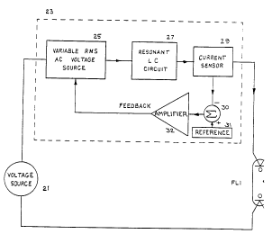
Fig. 4 is a block diagram of a high-impedance
device including both passive and active elements. Vari
able ac voltage source 25 provides ac voltage to resonant
LC circuit 27 at a frequency equal to or near its peak
response frequency. The resonant circuit provides current
to lamp FL1. Current sensor 29 senses the amount of
current through the lamp and provides a signal to summing
junction 30. Summing junction 30 compares this signal
with the signal from reference 31 and provides an error
signal proportional to the difference to amplifier 32.
Amplifier 32 adjusts variable source 25 to reduce the
difference between the signal from current sensor 29 and
reference 31, thereby reducing the magnitude of variations
in the current in lamp FL1 and increasing the circuit
output impedance. Thus, the equivalent output impedance of
this circuit is very high; much higher, in fact, than the
impedance of resonant LC circuit 27 alone. A dimming
circuit having a high-impedance device of this configura-
6232-90.CN -13-
/lp/#11
203057
tion with an equivalent output impedance of about 35,000
ohms was able to operate a compact fluorescent lamp at
light levels below about 1%.
Variable voltage source 25 can be any ac source
having a variable output voltage. This is preferably a
pulse-duration-modulated inverter circuit for producing ac
voltage pulses of variable duration. Alternatively element
25 may be a sinusoidal or square wave source of variable
amplitude. In another embodiment, element 25 may be
replaced with a constant-voltage source of variable fre-
quency.
Resonant LC circuit 27 can alternatively be re-
placed with any combination of resistive or reactive
components ox may be omitted completely. However, with a
relatively low impedance for element 27, the current sensor
29 must respond faster and amplifier 32 must have higher
gain in order to maintain the same equivalent output
impedance of high impedance device 23. As the speed of
response and gain of the system is increased, it becomes
mare difficult to avoid oscillation and provide suitably
stable operation. Alternatively, a relatively high value
of impedance for the passive element (in this ease resonant
circuit 27) allows lower gain and slower response, but
incurs more losses in the passive element.
Current sensor 29 may be any device that produces a
signal functionally related to a current flowing there-
through. This is preferably a low value resistor or a
small transformer.
One disadvantage of using a substantially symmetri
cal high-frequency waveform to operate fluorescent lamps is
the occurrence of visible striations along the length of
the lamp tube. These striations may be stationary ar they
may move in one direction or the other at various veloci
ties, and they are most commonly found when operating the
lamp below about 30% of nominal light output. We have
found that the addition of a small amount of do current or
6232-90.CN -14-
/lp/#11
202205?
low-frequency ac current can substantially reduce or
eliminate these visible striations.
Accordingly, Fig. 5A shows the ac component of
current flow through a fluorescent lamp according to one
embodiment of the present invention. The half period r is
determined by frequency of the sinusoidal current and is
preferably shorter than the de-ionization time of the gas
plasma. The RMS value of ac current to the lamp substan-
tially determines the power and, therefore, the brightness
of the lamp and is adjustable from a value approximately
equal to the nominal operating current of the lamp, the
value at which the nominal light output is obtained, to a
substantially lower value.
Fig. 5B shows the do component of current flow
through the lamp. For illustrative purposes, the magnitude
of the do component is exaggerated with respect to the ac
component. As a practical matter, for typical fluorescent
lamps, a do component of less than about 5% of the nominal
lamp operating current is preferred.
Fig. 5C shows the composite current waveform that
flows through the lamp. The do component offsets the ac
component from the zero current level, causing a slightly
asymmetric composite current waveform that substantially
reduces lamp striations. The frequency of the ac com-
ponent is preferably above 20kHz, so as to avoid audible
noise, although it is believed that lower frequencies will
still produce the desired result.
preferably, the do component is smaller than about
50 of the nominal lamp operating current so as to avoid the
aforementioned flickering and anode oscillation problems
associated with operating gas discharge lamps on do or
asymmetric ac current. The polarity of the do component
may be either positive or negative.
Tn another embodiment of the present invention, the
above described do component of current through the lamp
can be replaced by a low-frequency ac component. A chief
6232-90.CN -15-
/lp/#11
zo~zo5~
advantage of operating the lamp in this fashion is that
low-frequency ac sources are more readily available than do
sources.
The low-frequency current component is preferably
substantially lower than the pre:Eerred 27kHz frequency of
the driving voltage. Frequencies in the range between 30Hz
and 150Hz are preferred. Frequencies below 30Hz may cause
undesirable visible strobing of lamp brightness. Frequen-
cies much above 150Hz require increased amounts of low-
frequency current to reduce striations, but frequencies up
to at least about 5kHz are still useful.
Fig. 6 shows a composite current waveform having
both high-frequency and low-frequency ac components as
described above. The composite waveform can be described
as ac since it reverses polarity at regularly occurring
intervals and has alternately positive arid negative values.
The magnitude and relative frequency of the low-frequency
component is exaggerated for illustrative purposes.
The peak amplitude of the low-frequency component
is preferably less than that of the high-frequency com
ponent, such that the composite waveform reverses polarity
at a high-frequency over each low-frequency half-cycle.
The do component of the composite waveform as shown in Fig.
6 is preferably zero.
One convenient way of deriving a low-frequency
alternating current is illustrated in Fig. 7. In Fig. 7,
circuit elements given identical numbers are identical to
those described below in connection with Fig. 9, 10, and
11. Thus, front end rectifier 7, switching inverter 9 and
transformer T3 are identical to those elements as described
hereinafter. In Fig. 7, a portion of the 60Hz input
current is tapped off from the hot input H by a resistor
8100 between the hot input H and one side of the secondary
of transformer T3, where it is added to the high-frequency
alternating current supplied by the switching inverter 9 to
the lamp. The value of 8100 is chosen to provide any
6232-90.CN -16-
/lp/#11
zozzo~~
desired amplitude of the low-frequency component. A
capacitor C100 is connected from the junction of 8100 and
the secondary of transformer T3 to ground. For purposes of
this specification and the appended claims, when referring
to electrical elements, the term °'connected°' means that
there exists between two or more elements a conductive
path, which may include additional elements not explicitly
recited. C100 is chosen to provide a high ac impedance
path to ground at 60Hz so that the low-frequency alternat-
ing current injected into the secondary of transformer T3
flows through the lamp.
The low-frequency alternating current supplied to
the lamp provides an ac offset, rather than a do offset, to
the high-frequency alternating current supplied to the lamp
but still provides a degree of asymmetry to the high-
frequency current sufficient to substantially reduce the
occurrence of visible striations.
In addition to a 60Hz sinusoidal low-frequency
alternating current, other waveform shapes can be used,
such as square wave, triangular, saw-tooth, etc. A square
wave would, in effect, provide a positive do offset during
one half cycle and a negative do offset during the other
half cycle of the low-frequency alternating current, which
would render the high frequency current asymmetric during
both half cycles.
Moreover, it is not necessary that either a con-
stant direct current or a low-frequency alternating current
be used to eliminate visible striations in compact fluore-
scent lamps. Alternatively, a pulsating do current, such
as the pulsating do current from a full-wave rectifier, can
be used. One circuit for providing a pulsating do current
is shown in Fig. 8. In that circuit, one terminal of the
do side of the diode bridge FWB in front end rectifier 7 is
connected via resistor 8101 to one terminal of the secon-
dart' of transformer T3, where it is added to the high-
frequency alternating current supplied to the lamp by
6232-90.CN -17-
/lp/#11
X03205?
switching inverter 9. The pulsating do current waveform
derived from diode bridge FWB is shown in Fig. 8 as a
negative current, but it will be understood that a positive
current would also impart the desired asymmetry to the
high-frequency lamp current. The composite waveform
provided to the lamp, in this case, would contain do as
well as low-frequency and high-frequency ac components.
The pulsating do current derived from diode bridge
FWB may also, if desired, be converted to an asymmetric
low-frequency ac current by adding a do blocking capacitor
C101 in series with resistor 8101, as shown in Fig. 9. The
waveform of the low-frequency ac current is also shown in
Fig. 9, and is essentially the same waveform as described
above in connection with Fig. 8, but with a do component of
zero. It should be understood that the precise waveform
and the precise frequency are not critical. It should also
be understood that the single lamp shown can be replaced
with a plurality of series or parallel connected lamps.
It should additionally be pointed out that the
invention herein involved is not limited to the specific
circuit or waveforms as described above. Alternatively,
any type of current waveform having both ac and do com
ponents may be provided to the lamp to eliminate visible
striations.
Fig. 10 shows a block diagram of a dimming circuit
according to an embodiment of the present invention. The
dimming circuit 1, enclosed in the dashed lines, provides a
variable amount of power from sinusoidal power source 3 to
a gas discharge lamp 5. The dimming circuit generally
includes a front-end rectifier 7 to convert a typically
low-frequency ac voltage from power source 3 inter a do
voltage provided to switching inverter 9. Switching
inverter 9 converts the do voltage into a high-frequency ac
voltage consisting of alternately inverted and non-inverted
rectangular pulses of voltage having variable duration.
Pulse duration modulation (PDM) circuit 11 provides a
6232-90.CN -18-
/lp/#11
2032057
modulating voltage waveform to switching inverter 9 to
control the duration of each pulse.
The high-frequency ac voltage from switching
inverter 9 drives resonant circuit 13 so that it resonates
substantially sinusoidall_y, with an amplitude determined by
the amplitude and frequency of the driving voltage and the
magnification factor Q of the resonant circuit. The
resonant circuit is essentially a symmetrical high-frequen-
cy sinusoidal current source with a variable amplitude
determined by the pulse duration of the driving voltage
from switching inverter 9.
The current from resonant circuit 13 is provided to
lamp 5 to strike and maintain a stable electric discharge
over a range of selectable power levels. Simultaneously,
bank-end rectifier 15 rectifies a predetermined amount of
current from resonant circuit 13 and provides it to lamp 5,
adding to the current flow therethrough a do component
selected to minimize visible striations.
Current sensor 29 senses the amount of current
through the lamp and provides a signal to summing junction
30. Summing junction 30 compares this signal with the
signal from reference 31 and provides an error signal
proportional to the difference to amplifier 32. Amplifier
32 adjusts PDM control circuit 11 to reduce the difference
between the signal from current sensor 29 and reference 30,
thereby reducing the magnitude of variations in the current
in lamp FL1 and increasing the circuit output impedance.
Fig. 11 is a circuit schematic of one embodiment of
a dimming circuit according to the present invention. The
circuit operates as follows: ac voltage is provided from a
power source across hot (H) to neutral (N). Diodes D1 and
D2, resistor R1, capacitors C1 and C2, and zener diode Z1
comprise a low voltage do power supply. During each
positive voltage half-cycle, current flows from hot through
capacitor C1, diode D2, and capacitor C2 to neutral,
charging capacitor C2 plus(+) to minus(-), as shown.
6232-90.CN -19-
/lp/#11
203205?
Resistor R1 and zener diode Z1 regulate the output voltage
that appears across zener diode Z1 so that the power supply
is essentially a do voltage source having a do supply
voltage approximately equal to the breakover voltage of
zener diode Z1. Diode D1 provides a discharge path for
capacitor C1 during each negative voltage half-cycle.
Full-wave-bridge FWB rectifies ac voltage from the
power source and provides pulsating do voltage across the
output terminals (+) and (-). Pulsating do is filtered by
capacitor C3, which is connected across the output ter
minals of the full-wave-bridge. Resistor R2 is in parallel
with C3 and bleeds charge from it when power is removed.
Diodes D3, D4, D5, and D6, MOSFETS Q1 and Q2, resistors R3
and R4, transformer T1, and capacitor C4 comprise a switch-
ing inverter for switching and inverting filtered do
voltage into a high-frequency ac driving voltage. During
operation, capacitor C4 charges up to approximately half of
the voltage across capacitor C3. When Q1 is conductive, a
driving voltage is applied across the primary winding P of
transformer T2 that is positive and equal to the voltage
across C3 less the voltage across C4 (approximately half
the voltage across C3). When Q2 is conductive, the driving
voltage is inverted and equal to the voltage across C4.
When Q1 and Q2 are alternately switched at a high-frequency
(-27kHz), rectangular pulses of ac driving voltage are
produced having a peak-to-peak voltage substantially equal
to the voltage across capacitor C3.
The driving frequency is preferably between 2okHz
and 50kHz and is determined by the ac control voltage from
the PDM circuit, IC1, discussed below. Frequencies below
20kHz are in the human audible range and are therefore
undesirable. Frequencies above 50kHz are undesirable
because they tend to cause high thermal dissipation in
MOSFETS Q1 and Q2 and they increase the flow of leakage
current through the capacitive impedance of the fixture
6232-90.CN -20-
/lp/#11
2~32~5~
wires to ground, thereby making operation at low light
levels more difficult.
Resistors R3 and R4 damp oscillations which may
otherwise occur due to the leakage inductance of secondary
windings S1 and S2 of transformer T1 and gate capacitance
of MOSFETS Q1 and Q2. Diodes D3 and D4 block reverse
current from flowing through MOSFETS Q1 and Q2, respective-
ly. Diodes D5 and D6 provide a commutation path for
current flowing through Q2 and Q1, respectively.
Q1 and Q2 could be any type of semiconductor
switch, such as FETE or bipolar transistors; however,
MOSFETS, as shown, are preferred because of their fast
switching ability and their relatively low gate current
requirements. Alternatively, the switching inverter may be
replaced with a less-expensive semiconductor do frequency
converter, which converts a non°pulsating do voltage into a
high-frequency pulsating do voltage. An inverting type of
oscillating circuit, which converts do to ac, is preferred,
however, since it provides reduced peak magnetic flux in
the core of the power-carrying transformers for the same
amount of transformed energy, and provides a more symmetric
waveform.
Integrated circuit IC1, described below, receives
voltage (+VDC) from the do power supply and provides an ac
control voltage across the primary winding P of transformer
T1 to control the conductivity of MOSFETS Q1 and Q2 and,
accordingly, the duration of each rectangular pulse of
driving voltage. Secondary windings S1 and S2 of trans-
former T1 are arranged so that voltage is applied to the
gates of MOSFETS Q1 and Q2 in opposite polarities so that
only one device may be conductive at any given time.
Pulse-duration-modulated driving voltage is provided across
primary P of transformer T2 and across the resonant circuit
consisting of inductor L1 and capacitor C5 connected in
series. The resonant circuit rings substantially sinusoid-
ally at the driving frequency with an amplitude determined
6232-90.CN -21-
/lp/#11
~a3205'~
by the pulse duration of the driving voltage and the
magnification factor Q of the resonant circuit. The
magnification factor Q, in this case, is determined primar
ily by the impedance of lamps FL1 and FL2 , which load the
resonant circuit in parallel.
Loading the resonant circuit in parallel tends to
stabilize operation of the gas discharge lamps. In par-
ticular, as current through the lamps increases, lamp
conductivity increases, decreasing the magnification factor
Q of the resonant circuit and, thereby, reducing its
resonant response. Conversely, as the current through the
lamps decreases, lamp conductivity decreases, increasing
the magnification factor Q of the resonant circuit and,
thereby, boosting its resonant response. The resonant
circuit essentially behaves like an ac current source and
provides high-frequency sinusoidal current through trans-
former T3 to lamps FL1 and FL2. The magnitude of the
current is variable depending upon the pulse duration of
the driving voltage, and is sufficient to strike and
maintain an electric discharge in the lamps.
To further increase the stability of the resonant
circuit, the frequency of the driving voltage (~27kHz) is
less than the peak response frequency of the resonant
circuit (~33kHz). Alternatively, damping could be added to
the resonant circuit, reducing the magnification factor Q:
however, this would reduce its efficiency and generate
unwanted heat.
Capacitor C6, resistors R5 and R6, and diode D7
form a back end rectifier circuit for providing do current
through lamps FL1 and FL2 in series. Capacitor C6, con
nected between secondary windings S1 and S2 of transformer
T3, is selected to pass substantially all high-frequency
sinusoidal current from the resonant circuit to lamps FL1
and FL2. Resistor R6 allows do current to flow through
diode D7, providing a do offset to capacitor C6 so that the
sinusoidal current through lamps FL1 and FL2 receives a do
6232-90.CN -22-
/lp/#11
X03205?
component ef current, as determined by resistor R6.
Resistor R5 is essentially a bleeder to discharge capacitor
C6 when power is removed. Resistor R5 also limits the
amount of do offset on capacitor C6 when the conductivity
of the lamps decreases at low power levels.
Earth ground is referenced between secondary
windings S1 and S2 of transformer T3. The relative sizes
of the secondary windings are selected to provide suffi-
cient voltage with respect to ground to strike lamps FL1
and FL2 through the capacitance to ground of each lamp.
They are also selected to balance the ground currents
through each lamp so that the high-frequency sinusoidal
current energizes the lamps equally. In this particular
circuit, a compromise is necessary to achieve sufficient
striking voltage and, thus, the ground current through lamp
FLl is slightly larger than that through FL2. To correct
for this imbalance, capacitor C7 is provided in shunt with
lamp FL1 to provide compensating current to lamp FL2.
Capacitor C8 prevents high-frequency switching noise from
MOSFETS Q1 and Q2 in the switching inverter from adversely
affecting the light output of lamps FL1 and FL2.
Secondary windings S1, S2, and S3 of transformer T2
provide voltage to the filaments of lamps FL1 and FL2 to
heat them. Primary winding P of transformer T2 receives
pulse-duration-modulated voltage from the switching in-
verter circuit including MOSFETS Q1 and Q2. In addition,
after Q1 is turned off and before Q2 is turned on, current
through Q1 and inductor L1 commutates through diode D6,
turning it on. This provides across primary winding P of
transformer T2 an additional pulse of voltage, having an
amplitude equal to the voltage across capacitor C4. Once
the voltage across capacitor C5 reaches its peak, current
reverses through inductor L1, and capacitor C5 discharges,
turning diode D5 on. This provides across primary winding
P a second pulse of voltage, having an amplitude equal and
opposite to that of the first pulse. The two additional
6232-90.CN -23-
/lp/#11
CA 02032057 1999-04-20
voltage pulses substantially occupy the period of time
after Q1 is turned off and before Q2 is turned on. The
circuit behaves similarly during the period after Q2 is
turned off and before Q1 is turned on. The resultant high-
s frequency voltage across primary winding P has an RMS value
that is substantially constant throughout the dimming range
of the lamps. Thus, secondary windings S1, S2, and S3 also
provide constant RMS voltage to heat the filaments of lamps
FL1 and FL2 throughout the dimming range.
Integrated circuit IC1 is preferably an industry-
standard SG3526 pulse duration modulation (PDM) integrated
circuit. Internal operation of the integrated circuit is
described in the Silicon General Product Cataloa, 1989,
Section 4, pp. 111-110, and Section 12, pp. 49-74. Pins 14
and 17 of IC1 are connected to +VDC for receiving low
voltage do power from the do power supply circuit described
previously. Capacitor C13 is a bypass capacitor to help
maintain a steady do voltage on pins 14 and 17. Capacitor
C14 and resistors R9 and VR1 are connected to an internal
oscillator through pins 9 and 10 of IC1 and set the
modulation frequency. The combination of resistor R9 and
variable resistor VRl may optionally be replaced with a
single fixed resistor, but the combination, as shown, is
preferred as it allows easy adjustment of the modulation
frequency.
The output of IC1 consists of alternate pulses of
positive voltage provided on pins 13 av=~d 1.6 (outputs A and
B). This pulsating voltage is provided across input
terminals A and B of transformer T1 and controls the
conductivity of MOSFETS Q1 and Q2. The duration of each
pulse is preferably variable from zero to about 18~s, the
maximum pulse duration that still allows some dead time
between pulses at the preferred modulation Lrequency
(~27KHz). This dead time can be increased by connecting an
optional resistor (not shown) between pin 11 and ground.
Diodes D20 and D21, preferably Schottky diodes, prevent
6232-90.CN -24-
/lp/#11
~Q4~2~5?
outputs A and B, respectively, from being pulled excessive-
ly negative by the magnetizing current of transformer T1.
Integrated circuit IC1 preferably includes an error
amplifier for providing feedback control for the current
through lamps FL1 and FL2. To the negative sides of the
error amplifier is provided a voltage (-ERROR) that cor-
responds to the actual lamp current. To the positive side
of the error amplifier is provided a reference voltage
(+ERROR) set by potentiometer VR2, which may be part of a
dimming control, as shown. The output of the error ampli-
fier controls the pulse duration of outputs A and B and,
thus, controls the current through lamps FL1 and FL2. Vref
is a tightly regulated 5V supply produced on pin 18 of
integrated circuit IC1.
A current sensing circuit, comprising diodes D8,
D9, D10, and D11, resistors R7, R8, and R14 and capacitor
C17 provides a voltage (-ERROR) that is indicative of the
lamp current. The current sensing circuit operates as
follows: During each positive half-cycle of current flow
(iFL) through the lamps FL1 and FL2, current flows through
capacitor C6 and diode D8. During each negative half-
cycle, current flows through capacitor C6, diode D9,
resistor R7 and either resistor R8 or series connected
diodes D10 and D11.
At low current levels, the voltage drop across
resistor R8 is too small to turn on diodes D10 and D11. In
this case, the voltage (-ERROR) varies proportionally with
the lamp current and the sum of the resistances R7 and R8.
At larger currents, diodes D10 and D11 turn on and provide
a substantially constant voltage drop that is independent
of the lamp current (iFL). The voltage (-ERROR) in this
case, varies proportionally with the lamp current and the
resistance R7.
Fig. 12 shows the resulting relationship between
lamp current (iFL) and the feedback voltage (-ERROR). The
dual slope characteristic of this relationship allows for
6232-90.CN -25-
/lp/#11
202205?
high sensitivity and tight control of lamp current at low
current levels, resulting in high output impedance at low
current levels and low power dissipation in the sensor
resistors at high current levels. Resistor R7 preferably
has less resistance than resistor R8. A resistance ratio
of about 4:1 is preferred for full-range control of most
types of compact fluorescent lamps. Diodes D8 and D9 are
preferably fast recovery diodes. Resistor R14 and capaci-
tor C17 increase the stability of the feedback control
system by attenuating any ac voltage components provided to
pin 2 of integrated circuit IC1.
Since certain changes may be made in the above
described embodiments without departing from the scope of
the invention herein involved, it is intended that all
matter contained in the above description or shown in the
accompanying drawings shall be interpreted in an illustra-
tive and not a limiting sense.
6232-90.CN -26-
/lp/~#11