Note: Descriptions are shown in the official language in which they were submitted.
20323~
TITLE OF THE INVENTION
Picture digitizing system
BACKG~OUND OF THE INVENTION
1. Field of the Invention
The present invention relates to a picture
digitizing system which is effective when it is desired
to reproduce a picture having a half-tone level with
use of, for example, a dot printer or the like.
2. Description of the Related Art
Such a picture having a half-tone level as a
photograph picture has been recently output and
displayed with use of such a simple binary recorder as
a dot Printer. Since this sort of recorder cannot
provide multiple display states more than two display
states, white and black, it becomes necessary to
effectively convert the above half-tone picture into
binary one. With regard to the binary Processing, for
example, for photographs on new~papers, various screens
having different net sizes are used to provide a
varying density effect to the photograph. However, the
employment of this method to the dot printer or the
like as it is involves difficulties.
To avoid these difficulties, it has been common
practice to typically introduce such an organization
dither method or a mean error least method to convert a
half-tone picture into binary one. In the organization
dither method, a suitable threshold level is previouslY
set for pixel positions and a pixel signal is
"
- ., . ', ' , .:
", .
"- ., "' ' ' -', ' ~
- 20323~2
discriminated and converted into binary one on the
basis of the threshold level. However, this
organization dither method is inferior to the above
mean error least method in picture quality. In the
mean error least method, on the other hand, binary
processin~ (conversion to binary data) is determined so
that an average of differences between an original
picture and binary pictures each made of a plurality of
picture elements (pixels) in small zones of the
original picture becomes small. This mean error least
method however has a defect that, though the method can
provide improved picture quality, the binary processing
is complex and thus requires a large-scale system
arrangement.
In view of such circumstances, there has been
proposed ~uch a picture digitizin~ system as taught in
Japanese Patent Appln. Laid-Open No. 57-104369 wherein
an average density approximation method for converting
a half-tone picture to a binary picture is used to
obtain the binary picture of a picture quality
comparable to that obtained by the mean error least
method, and also which can be inexpensively realized
with a simple hardware arrangement. In this sYstem~
the binary conversion is carried out on the basis of an
area ratio of black dots occupied in a small zone,
i.e., an average density. The average densitY is
calculated with respect to a dot to be converted to a
binary dot as well as already-converted binary dots
20323~
arranged around the former dot, and the decision of
whether the dot to be converted is black or white is
made by computing an average density of the dot to be
converted when it is black and an average density
thereof when it is white, checking which is closer to
that of the input signal and employing the closer one.
However, the above picture digitizing system has
had a problem that, when the system reads or inputs
such a picture having a regularly varying density or a
constant density as artificiallY created, a regular
read level continues and therefore its output dot
pattern becomes similar, which results in that the
picture qualitY is deteriorated.
In addition, the prior art system has been
disadvantageous in that, when picture reproduction is
carried out through the conversion of density, r
characteristics and so on of the picture, the binary
conversion and then the picture processing must be
performed, thus requiring a large size of hardware.
SUMMARY OF THE INVENTION
It is an object of the present invention to
provide a picture digitizing sy~tem which can eliminate
the above problems in the prior art and can avoid the
deterioration of a picture quality even when reading
such a picture having a regularly varying den~ity or a
constant density as artificially created.
Another object of the present invention is to
provide a picture digitizing system which can perform
,: ' ,,, ' ' :
' " ' ' , ~
: .
.. ,, . - ,
20323~2
picture processings at a time, thus realizing its small
scale hardware.
In accordance with an aspect of the present
invention, binary threshold data for comparison with a
current picture signal is randomly varied within a
predetermined range to slightly change the binarY
threshold data within such a picture level range that
users cannot recognize, whereby the regular binarY
pattern can be prevented from continuously appearing.
As a result, there can be provided a picture digitizing
system which, even when the system inputs such a
picture having a regularly varying or constant densitY
as artificially created, can avoid the deterioration of
the picture qualitY.
In accordance with another aspect of the present
invention, a binary threshold data for comparison with
a current input picture signal is changed according to
a desired density to obtain a binary picture signal
corresponding to the desired density. With such an
arrangement, the conversion processings of density, r
characteristics and so on of the picture can be carried
out at a time during creation of the binary threshold
data, whereby its hardware can be reduced in size to a
large extent.
BRIEF DESCRIPTION OF THE DRAWINGS
Fig. 1 is a block diagram of a picture digitizing
system in accordance with an embodiment of the pre~ent
invention;
2~3234~
Fig. 2 shows diagrams for explaining the
conception of pixel unit and picture processing:
Fig~ 3 is a diagram for explaining an example of a
weight factor;
Fig. 4 is a block diagram of another embodiment of
the invention wherein a ROM and a comparator in the
embodiment of Fig. 1 are replaced by a ROM;
Fig. 5 is a block diagram of an example of the ROM
in Fig. 1 constituted as a computation circuit;
Fig. 6 is a block diagram of a further embodiment
of the invention wherein conversion processings of
density, r characteristics and so on of a picture are
carried out at a time during creation of binary
threshold data;
Fig. 7 is a block diagram of yet another
embodiment of the invention wherein a ROM and a
comparator in the embodiment of Fig. 6 are replaced by
a ROM;
Fig. 8 is a block diagram of yet a further
embodiment of the invention wherein the storage
capacitY of a ROM can be made small;
Fig. 9 i9 a block diagram of other embodiment of
the invention wherein a ROM and a comparator in the
embodiment of Fig. 8 are replaced by a ROM;
Fig. 10 is a block diagram of other embodiment of
the invention which can be suitably made in the form of
a gate array;
Fig. 11 is a block diagram of an exemPlary
- '~
' -,. ' '
2a323~2
arrangement of a weighter in Fig. 10;
Fig. 12 is a block diagram of other embodiment of
the invention wherein the arrangement of Fig. 10 is
employed in the arrangement of Fig. 6; and
Fig. 13 is a block diagram of another embodiment
of the invention wherein the arrangement of Fig. 10 is
employed in the arrangement of Fig. 6.
DESCRIPTION OF THE PREFERRED EMBODIMENTS
The present invention will be described in
connection with embodiments of the invention by
referring to the accompanying drawings.
Explanation will first be made as to the principle
of how to digitize picture data employed in the present
embodiments.
Figs. 2(a) and 2(b) sho~ diagrams for explaining a
relationship between a half-tone picture 1 and a
picture element (pixel) 2 extracted and sampled from
the picture 1 through raster scanning operation of the
picture 1, wherein Fig. 2(a) is a general arrangement
and Fig. 2(b) is an enlarged view of a part thereof.
When an input picture is defined as f(i,j) and
binary data at the picture position (i,j) is as binary
data g(i,J), the following relationships are satisfied.
O S ~(i, j) ~ 1 1
g(i,j) = 1 J (1)
These relation~hips mean that the input picture f(i,;)
... ,~ -. . . .
203234~
at the picture position (i,i) has a normalized level
between O and 1 while the binary data g(i,j) takes a
value O or 1 with respect to the level of the input
picture. In Fig. 2(b), a pixel 2a shown bY a hatched
area corresponds to data at a position to be processed
and pixels 2b indicate binary data already subjected to
a digitizing processing, and pixels 2c indicate non-
processed pixels. The pixels 2b are extracted from two
previous pixels of the picture 2a and five pixels of
each of two previous lines of the pixel 2a, and the
pixels 2c are extracted from two proceeding Pixels of
the pixel 2a. Assume that Q denotes a set of already
processed pixels 2b and Q' denotes a set including the
Q and the pixel 2a to be processed. Then the
digitizing algorithm of the present system is
expressed as follows.
g(M,N) = F{f(M,N), g(i,j)[(i,j)~ Q]} -(2)
where, the coordinate (M,N) indicates a position
of a Pixel to be processed and F is a function. That
is, the binary data g(M,N) at the pixel position (M,N)
to be processed iq determined by a certain weight
function F on the basis of input picture signal data
f(M,N) at the pixel position (M,N) and binary data
g(i,~) already digitized at an adjacent pixel position
(i,j). The function F is given, for example, as
follows.
: . . , , . , ~ . ;
... ..
2032342
l-- X~ 1/2~ (0,0)
g(M,N) = F(x) = {
O- X< 1/2a (0,0) -(3)
where X is expressed as follows.
X = { a (M-i, N-j)}- f(M,N)
(i,j)~ Q'
- ~ a (M-i,N-j)- g(i,j)
(i,j)~ Q
where a (i,j) denotes a weight function having such
weights, for example, as shown in Fig. 3. As shown by
this algorithm, when the weight function is merely
previously set, binary data for the above picture
signal data can be created easily on the basis of the
previous (past) binary data and the input picture
signal data at the current coordinate position. In
addition, since the past data necessary for the
digitizing processing are all binary data, the storage
of such past data can be facilitated.
As will be clear from the equation (3), in the
aforementioned system, the binary data g(M,N) is
obtained by finding the value of X in accordance with
the above equation and comparing the found X with the
factor a (0,0). In other words, it is Judged whether
or not the following relationship is sakisfied.
.. - :~ , . ., , .......................... :. ...
. . : ::: .
-:
2032342
~ a (M-i,N-j)}- f(M,N)
(i,j)~ Q'
-~ a (M-i,N-j)- g(i,j)~ 1/2a (0,0)
(i,j)~Q --(4)
When attention is paid to the expression (4), the
following relationship (5) can be obtained.
a (M-i,N-j)- g(i,j)
(i,j)~ Q 1/2a (0,0)
f(M,N) -
a (M-i,N-j) ~ a (M-i,N-j)
(i,j)~ Q' (i,j)~Q'
(5)
Hence, when it is judged whether the followin~ relation
(6) is satisfied, the binary data g(M,N) can be
directly obtained.
S a (M-i,N-j) g(i,j) + 1/2a (0,0)
(i,~)6Q
f(M,N) ~
s.~ (M-i.N-j)
(i,j)~Q'
(6)
Thus, the right side of the above expression is
.- :. - , :
: . - . . ,
20323~2
expressed as the past data g(i,j).
According to this system, however, in the event
where read half-tone level has a regularitY or a
uniform constant density is continued, the value of the
left side of the above expression can be very close to
the value of the right side thereof. Thus, the similar
pattern appears repetitively and becomes noticeable~
which leads to deterioration in the picture quality.
In order to avoid this, in accordance with the
present invention, a very low density level ~ is added
to the right side of the expression (6), as shown by
the following expression (7).
a (M-i,N-j) g(i,j) + 1/2a (O, O)
(i,j)~Q
f(M,N) ~ +
a (M-i,N-j)
(i,j)~Q'
(7)
where
a (M-i,N-j)
a (M-i,N-j)
(i,j) Q'
(8)
In the expression (8), a (M-i,N-j3 is a condition
for its possible minimum value.
, ' .' ~ .,
' ' ~
'~
2032342
With such an arrangement, it can be prevented that such
a relationship as mentioned above collapses and the
similar pattern repetitively appears, thus preventing
the deterioration of the picture qualitY.
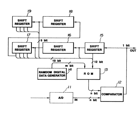
Referring now to Fig. 1, there is shown a block
diagram of a picture digitizing system in accordance
with an embodiment of the present invention which
realizes the aforementioned algorithm. An input
picture signal obtained through the line scanning
operation of a half-tone picture is converted into
digital data of n bits through, for example, an A/D
converter 11. The digital data is sent from the A/D
converter to a comparator 12 to be compared with binary
threshold data of n bits received at the comparator
from a read-only memory 13 (ROM) to be described later.
The comparator 12, on the basis of the comparison
result, outputs binary digital data corresponding to
the input picture signal. Between the A/D converter 11
and the comparator 12, needless to say, such a picture
correction circuit as, for example, a shading
correction circuit or an automatic gain correction
circuit may be provided as necessary. The ROM 13
receives binary digital data of 12 bits to be explained
later and random digital data of m bits as address data
from a random digital data generator 14, and outputs
the aforementioned binary threshold data of n bits
created in accordance with the foregoing algorithm.
The binary data of one bit issued from the
.
-: ,
.: : ,
,,
.
20323~2
comparator 12 is supplied to a predetermined output
apparatus (not shown) and also through a shift register
15 (where the input data is delayed by twice its
sampling time) sequentially to shift registers 16, 17,
18 and l9.The shift registers 16 and 17, which are
connected in series with each other, act to delay the
one-bit digital data by one line scanning time period,
and the latter-stage shift register 17 outputs from its
taps one-bit binary data at adjacent, say, 5 sample (5
pixel) positions on a parallel basis. 3imilarly, the
shift registers 18 and 19, which are connected in
series with each other, act to delay their input signal
by one line scanning time period, and the latter-stage
shift register 19 outputs from its taps one-bit binary
data at the 5 sample positions. A total of 12 bits of
~uch parallel data parallelly extracted from these
shift registers 15, 17 and 19 are used as the
aforementioned address data of the ROM 13.
More in detail, when an output of the A/D
converter at a time to is picture signal data of n bits
(CO, Cl, C2,..., and Cn_l), the shift register 15
outputs, at the time to, one-samPle previous binary
data D-1 and two-sample previous binary data D-2.
Further, when the number of samples to be processed
through one l~ne scanning operation is L, the parallel
outputs of the shift register 17 correspond to binary
data D-CL-:-). D-~L-1). D-L. D-~L~1). D-~L~2). Whereag
the parallel outputs of the shift register 19
.. . .
: . ; ,
,:.
.
20323~
correspond to binary data D- C2~-2,, D- (2~ D-2~, D-
(2~ . , . D- (2~, 2, . Therefore, the ROM 13 receives 12
bit data of D-1, D-2. D-(T-2> to D_(~+2,, and D_(z~_2,
to D_(2~,2, as well as random digital data of m bits
from the random digital data generator 14, i.e., a
total of (12+m) bits of data.
The data CO to C~_l correspond to f(M,N) in the
aforementioned algorithm, while the 12-bit data D-1~ D-
2, D_(~_2, to D_(~,2 " and D-(2~-2, to D_(2~+2,
correspond to g(i,j)[i,j~ Q].
Binary threshold data of n bits previously
registered in the ROM 13 is calculated and created in
accordance with the aforementioned algorithm, and the
random digital data of m bits issued from the random
digital data generator 14 is used to randomly select
the previously-created binary threshold data of the ROM
13 having slightly different density levels. The m-bit
random digital data varies from pixel to pixel and how
to generate this data and the size of the m are
arbitrary.
Although the shift registers have been used to
provide the line delay to the binary data in the
foregoing embodiment, the binary data may be stored in
a random access memory (RAM) to be controlled by an
address controller. Further, the comparator 12
per~orms itR comparison operation with recpect to the
n-bit digital data, but the comparator 12 may be
replaced by an analog comparator to directlY input the
13
, . . , :
:
- , .
` 20323~2
input picture data without the intervention of the A/D
converter 11, whereby the n-bit digital data from the
ROM 13 is converted into an analog data through a D/A
converter for the comparison at the analog comparator.
Shown in Fig. 4 is another embodiment of the
present invention, in which the ROM 13 and the
comparator 12 in Fig. 1 is rePlaced by a ROM 20. In
the present embodiment, the ROM 20 receives a total of
(12+m+n) bits of data, that is, a total of 12 bits of
parallel data parallelly issued from the shift
registers 15, 17 and 19, the random digital data of m
bits from the random digital data generator 14, and the
data of n bits from the A/D converter 11; and outputs a
desired binary picture signal. Other arrangement is
substantial 1Y the same as that shown in Fig. 1.
In the foregoing embodiment, such Past binary data
as a pixel zone Q and a pixel number fed back in the
binary processing as well as the weight function ~ and
the very low density level ~ can be determined
according to the application specifications and the
pre~ent invention is not limited only to the foregoing
arrangement. Further, although the very low densitY
level o~ has been randomly added, the level ~ may be
added randomly only when the level is continuously
constant or according to a predetermined method, or the
level ~ may not be added but multiplied by a
predetermined value. In addition, the very low densitY
level ~ has been added to the binary threshold data,
14
.
-' , ~,
.
- ,
20~23~
but it may be added to the input picture signal, as a
matter of course.
Though computation data have been previously
registered in the ROM 13 in the embodiment of Fig. 1,
the embodiment may be arranged so that the ROM is not
used and computation is carried out each time.
The latter case is shown in Fig. 5 as a further
embodiment of the present invention. In the drawing, a
computation circuit 130 receives 12 bits of signals
from the shift registers 15, 17 and 19 as well as an m
bits of signal from the random digital generator 14.
The computation circuit 130 includes 12 multipliers Ml
to M12, 12 weight factor setting circuits Wl to W12 and
a single adder AD, and performs the operation
corresponding to the right side of the equation (6).
The present embodiment is arranged so that the random
digital generator 14 of Fig. 1 generates such a signal
that the value l/2a (0,0) is taken into consideration
and the A/D converter 11 of Fig. 1 outputs a signal
including the value of a denominator of the right side
of the equation (6).
In this way, in accordance with the embodiments of
Figs. 1 to 5, there can be provided such picture
digitizing systems of relatively simple arrangements
that, even when reading ~uch a picture having a
regularly varying density or having a constant density
as created artificially, can prevent the deterioration
of the picture quality.
",
" ' .
2~323~
In an average-density approximation method shown
in the equation (6), when it is desired to reproduce
the picture through the conversion of the density, r
characteristics and so on of the picture, the density
conversion is previously carried out in the previous-
stage and then the picture processing is carried out.
Thæt is, when the input picture f(M,N) is subiected to
a density level conversion, an algorithm shown in the
following expression (9) is carried out.
f(M,N)- h(M,N)~
a (M-1,N-j) g(i,j) + 1/2a (0,0)
(i,j)~ Q
~ a (M-i,N-j)
(i,J)~ Q'
(9)
From the above equation, the following expression
is obtained.
f(M,N)
~ a (M-i,N-j) g(i,j) + 1/2a (0,0)
(i,~)~ Q
,
~ a ~M-i,N-~) h(M,N)
(i,j)~Q'
( 10)
Thus, it will be seen that a picture to be reProduced
16
' . : : , ..... ...
20323Q~2
can be reproduced by converting the density, r
characteristics and so on of the reproduction picture
during creation of binary threshold data.
Fig. 6 shows a block diagram of a picture
digitizing system in accordance with a further
embodiment of the present invention realizing the
aforementioned algorithm. In the arrangement of the
system of Fig. 6, the random digital data generator 14
in Fig. 1 is replaced by a density conversion selector
14a which outputs density threshold selection data of m
bits to a ROM 131 as its address data. Other
arrangement is substantially the same as that of Fig.
1.
In accordance with the present embodiment, there
can be provided a picture di~itizing system which can
be realized inexpensively with a relatively simple
arrangement and can perform conversion over the
density r characteristics and so on of a picture at a
time during generation of binary threshold data. thus
enabling the remarkable reduction of size of its
hardware.
Although the shift registers have been used to
provide the line delay to the binary data in the
cmbodiment of Fig. 6, the line delaY of the binary data
may be achieved bY storing the binary data in a random
access memory (RAM) to be controlled by an address
controller. Further, the comparator 12 performs its
comparison operation with respect to the n-bit digital
17
' ' . ~ ' .
20323~2
data, but the comparator 12 may be replaced by an
analog comparator to directly input the input picture
data without the intervention of the A/D converter 11,
whereby the n-bit digital data from the ROM 131 is
converted into an analog data through a D/A converter
for the comparison at the analog comparator.
The foregoing embodiment can have substantially
the same effect as that of Figs. 1, 4 and 5 when the
binary threshold data is varied within a predetermined
range with the arrangements of Figs. 1, 4 and 5.
Referring to Fig. 7, there is shown yet another
embodiment of the present invention, wherein the ROM
131 and the comparator 12 in Fig. 6 are replaced by a
ROM 201. In the present embodiment, the ROM 201
receives a total of (12+m+n) bits of data, that is, a
total of 12 bits of parallel data parallelly issued
from the shift registers 15, 17 and 19, the density
threshold selection data of m bits from the densitY
threshold selector 14a, and the data of n bits from the
A/D converter 11; and outputs a desired binary picture
signal. Other arrangement is substantially the same as
that shown in Fig. 6.
In the foregoing embodiment, such past binary data
as a pixel zone Q and a pixel number fed back in the
binary processing as well as the weight function ~ and
the density conversion function h(M,N) can be
determined according to the application specifications.
Further, in place of the ROM having the computation
18
. .
2~32~
data previously registered therein, such a computation
circuit as shown in Fig. 5 may be used to perform the
computation each time.
In the foregoing embodiment, when it is desired to
realize the system shown by the equation (6), address
bits corresponding in number to the past binarY data
g(i,j) are necessary, because the computation of the
right side of the equation (6) is carried out bY
previously registering the computation data in the ROM
and making access to the data with use of the past data
g(i,j).
A term which follows in the equation (6):
a (M-i,N-j) g(i,j)
(i,j)~Q
corresponds to a sum of multiplication results of the
pixel g(i,j) (black pixel 1, white pixel O) is
multiplied by such a weight factor a (M-i,N-j) as shown
in Fig. 3. However, for example, such a sum may be
obtained bY combining terms corresponding to pixels
having the same weight factor ~ (M-i,N-j) and
multiplying the number of black pixels g(i,j) by the
weight factor a (M-i,N-j).
Fig. 8 schematically shows an arrangement of the
latter case as yet a further embodiment of the present
invention, in which an input picture signal obtained
through the line scanning operation of a half-tone
.
20323~
picture is converted into digital data of n bits
through, for example, an A/D converter 11. The digital
data is sent from the A/D converter to a comparator 12
to be compared with binary threshold data of n bits
received at the comparator from a read-only memory 132
(ROM) to be described later. The comparator 12, on the
basis of the comparison result, outputs binary digital
data corresponding to the input picture signal.
Between the A/D converter 11 and the comparator 12,
needless to say, such a picture correction circuit as,
for example, a shading correction circuit or an
automatic gain correction circuit may be provided as
necessary.
The ROM 132 receives binary digital data of 10
bits to be explained later as address data, and outputs
the aforementioned binary threshold data of n bits
created in accordance with the foregoing algorithm.
The binary data of one bit issued from the
comparator 12 i9 suppl ied to a predetermined output
apparatus (not shown) and also through a shift register
15 (where the input data is delayed by twice its
sampling time) sequential 1Y to shift registers 16, 17,
18 and 19. The shift re~isters 16 and 17, which are
connected in series with each other, act to delay the
one-bit digital data by one line scanning time period,
and the latter-sta8e shift register 17 outputs from its
taps one-bit binary data at adjacent, say, 5 sample (5
pixel) positions on a parallel basis. Similarly, the
20323~2
shift registers 18 and 19, which are connected in
series with each other, act to delaY their input signal
by one line scanning time period, and the latter-stage
shift register 19 outputs from its taps one-bit binary
data at the 5 sample positions.
In Fig. 8, the shift registers 15, 16, 17, 18 and
19 as well as the A/D converter 11 have the same
functions as those having the same reference numerals
in-Fig. 1.
In the present embodiment, the total of 12 bits of
data parallelly taken from the shift registers 15, 17
and 19 are combinedly input to counters 21, 22, 23 and
~4 which count the numbers of black pixels and apply
the counted results to the ROM 132 as its address data.
More in detail, when an output of the A/D
converter at a time to is picture signal data of n bits
(CO, Cl, Cz,..., and Cn-l)~ the shift register 15
outputs, at the time to, one-sample previous binary
data D-1 and two-sample previous binary data D-2.
Further, when the number of samples to be processed
through one line scanning operation is L, the parallel
outputs of the shift register 17 correspond to binary
data D-~L-2). D-~L-1~. D-L~ D-~LI1). D-~LI2). Whereag
the parallel outputs of the shift register 19
corre~pond to binary data D-~2L-Z). D-~2L-1). D-2L. D-
~ZL~1) . D--~ZL~2) .
Thus, in the case where such a weight factor
matrix as shown in Fig. 3 is employed for example, the
21
2032342
counter 21 receives the binary data D_~2~-2, and D-
(2~+2~ of two bits corresponding to weight factor 1 and
outputs the then counted result of 2 bits for black
pixels to the ROM 132; the counter 22 receives the
binary data D_~2~-l" D-c2~ D_(~-2~ and D_~+2~ of
four bits corresponding to weight factor 3 and outputs
the then counted result of 3 bits for black pixels to
the ROM 132; the counter 23 receives the binary data D_
2 , D_~_l, D~ and D_2 of four bits corresponding
to weight factor 5 and outputs the then counted result
of 3 bits for black pixels to the ROM 132; and the
counter 24 receives the binary data D_~ and D_l of two
bits corresponding to weight factor 7 and outputs the
then counted result of 2 bits for black pixels to the
ROM 132.
The data CO to Cn_l correspond to f(M,N) in the
aforementioned algorithm, while the 12-bit data D_l, D-
z, D_c~_z) to D_c~,z~, and D_c2~_2~ to D_cz~,
correspond to g(i,j)[i,j~Q].
Binary threshold data of n bits previously
registered in the ROM 132 is calculated and created in
accordance with the aforementioned algorithm.
Although the shift registers have been used to provide
the line delay to the binary data in the foregoing
embodiment, the binary data may be stored in a random
access memory (RAM) to be controlled by an address
controller.
Shown in Fig. 9 is other embodiment of the present
22
,....
,.~ .
20323~
invention, in which the ROM 132 and the comparator 12
in Fig. 8 are replaced by a ROM 202. In the present
embodiment, the ROM 202 receives a total of (lO~n) bits
of data, that is, the measured data of 10 bits from the
counters 21, 22, 23 and 24 as well as data of n bits
from the A/D converter 11, and outputs a desired binary
picture signal. Other arrangement is substantiallY the
same as that of Fig. 8.
In the embodiments of Figs. 8 and 9, the average
density is obtained not by inputting the alreadY-
digitized binary dot data in the ROM at its address as
it is but by counting or computing the numbers of black
pixels in the binarY dot data having the same weight
factors and inputting the counted results in the ROM,
so that, even when the pixel zone Q is expanded, it is
unnecessary to expand the zone of the memory ROM and
the zone can be used without any change. In this way,
the embodiments of Figs. 8 and 9 are highly effective.
In other words, the necessary capacity of the memory
ROM can be made small. This is very important in that,
when it is desired to make the system in the form of a
gate array, the counters can be built in the gate array
but the ROM cannot be incorporated therein and must be
provided as an external device of the gate array.
In the embodiments of Figs. 8 and 9, the binary
threshold data may be varied as shown in Figs. 1, 4, 5,
6 and 7.
In each of the foregoing embodiments, in makin~
23
203~3 ~
the hardware part of the system in the form of a gate
array, it sometimes becomes difficult to make the ROM
part for computation of the average density in the form
of the gate array because of its large amount of data.
To avoid such a difficultY, the computation of the
average density effected in the ROM part is arranged to
be carried out by a hardware comprising simple adders
and flip-flops, whereby the formation of the gate array
can be readily achieved and a high-speed processing can
be realized. This is shown in Fig. 10 as other
embodiment of the present invention.
In the present embodiment, the adders and the
flip-flops are used to perform sequential addition of
weighted binary data to thereby create binary threshold
data for the current input picture signal. As a
result, any ROM part can be eliminated, the formation
of the system in the form of a gate array can be
facilitated and the high-speed processing can be
realized.
The above arrangement of the foregoing embodiment
of the present invention is schematically shown in Fig.
10. An input picture signal obtained through the line
scanning operation of a half-tone picture is converted
into digital data of n bits through, for example, an
A/D converter 11. The digital data of n bits is sent
from the A/D converter to a comparator 12 to be
compared with binary threshold data of n bits received
at the comparator from an adder 31 to be described
24
.
`" 203~342
later. The comparator 12, on the basis of the
comparison result, outputs binary digital data
corresponding to the input picture signal. Between the
A/D converter 11 and the comparator 12, needless to
say, such a picture correction circuit as, for example,
a shading correction circuit or an automatic gain
correction circuit may be provided as necessary.
The binary one-bit data issued from the comparator
12 is supplied to a predetermined output device (not
shown) and also to weighters 33 and 34 and a one-line
delay unit 66. The one-line delay unit 66, which
functions to delay the binary pixel result by a time
corresponding to one line, comprises a random access
memory (RAM) which is controlled bY an address
controller (not shown). An output of the one-line
delay unit 66 is supplied to weighters 35, 36, 37, 38
and 39 and also to a one-line delay unit 67. The one-
line delay unit 67, which functions to delay the binary
result by an additional time corresponding to one line,
whereby the binary result is delayed by a time
corresponding to a total of two lines. An output of
the one-line delaY unit 67 is supplied to weighters 40,
41, 42, 43 and 44.
In the weighters 33 and 34, the weight factor ~
(M-i,N-J) in a term in the right side of the equation
(6) is superimposed on the binary result g(i,j), That
iq, a (M-i,N-J) g(i,i) is computed.
Shown in Fig. 11 is an example of the arrangement
' ' ,,
.
203~3~2
of the weighters 33 to 44. This example shows a weight
factor a (M-i,N-j) comprising 4 bits. Since the binarY
data g(i,i) already digitized is of one bit, a (M-i,N-
j) g(i,j) is computed by performing a logical "AND"
operation of the respective bits. Thus, the example
may comprise only four AND gates ANl to AN4.
Turning again to Fig. 10, flip-flops 45 to 56 are
used to shift the computation result sequentially one
pixel after another and the shifted result is
sequentially added at adders 57 to 65.
The weighters 33 to 44 have weight factors of ~
(2,0), a (1,0), a (2,1), a (1,1), a (0,1), a (-1,1), a
(-2,1), a (2,2), a (1, 2), a (O, 2), a (-1, 2), and al(-
2,2) associated with Fig. 3(b), respectively. More
specifically, when such a weight factor matrix as shown
in Fig. 3 is emPloyed, the order of the weight factors
is 5, 7, 3, 5, 7, 5, 1, 3, 5, 3 and 1.
For example, the output of the flip-floP 45
becomes a (2,0)- g(M-2,N), while the output of the
flip-flop 46 becomes a (2,0) g(M-2,N) + a (1,0) g(M-
l,N). And the output of the flip-flop 51 becomes a
(2,1) g(M-2,N-l) + a (1,1)- g(M-l,N-l) + a (0,1)
g(M,N-l) ~ a (-1,1) g(M+l.N-l)+ a (-2,1) g(M+2,N-l);
wherea~ the output of the flip-flop 56 becomes a (2,2)
g(M-2,N-2) + a (1, 2) g(M-l,N-2) ~ a (O, 1) g(M,N-2)
+ a (-1. 2) g(M+l,N-2) + a (-2.2) g(M+2,N-2).
Eventually, these results are added together at an
adder 32 to obtain the following part in the right side
26
2Q32342
of the equation (6).
a (M-i,N-j) g(i,j)
(i,j)~Q
The result is input to the adder 31 to be added to 1/2
a (O, O) in the right side of the equation (6). An
addition output of the adder 31 is input to the
comparator 12. Transposing the numerator of the right
side of the equation (6) to its left side results in:
a (M-i,N-j)- f(M,N)~ -
(i,j)~Q'
a (M-i,N-j)- g(i,j) + 1/2a (0,0)
(i,j)~Q --(11)
The right side of the equation (11) corresponds to the
output of the adder 13. The input picture f(M,N) is a
picture at the picture position (M,N) and has a
normalized level between O and 1.
S,a (M-i.N-j)
(i,j) Q'
This means a sum of weight factors. When the weight
factor sum is set to be the maximum number of tones in
picture data, the left side of the equation (11)
corresponds to the level itself of the input picture
and thus the input picture level can be compared at the
27
-- 20323~2
comparator 12 directly with the threshold level
received from the adder 31 as alreadY explained above.
Fig. 12 shows other embodiment of the present
invention, wherein a register 70 for storing therein a
part, i.e., l/2a (O,O), in the right side of the
equation (6) in Fig. 10 is replaced by a register 71
for storing therein a density correction value, In the
present embodiment, the same density correction method
as employed in Fig. 6 is employed. Since the present
embodiment is arranged to add the densitY correction
value to the binary threshold value, a picture can be
reproduced through the conversion of the density, r
characteristics and so on thereof.
For example, adding a correction value h(M,N) to
the right side of the equation (11) results in:
a (M-i,N-j)- f(M,N)~
(i,j)~Q'
a (M-i,N-j)- g(i,j) + 1/2a (O,O) + h(M,N)
(i,j)~Q
(12)
It will be appreciated that, when the correction value
h(M,N) is transposed to its left side, the left side
lndicates the value of intensity of the input picture
and thus the density is converted. Further, the
correction value h(M,N) should be preferably a
correction value when the coefficient 1/2~ (O,O) is
taken into consideration. Other arrangement is
^` 2~3234~
substantially the same as that of Fig. 10.
Referring further to Fig. 13, there is shown other
embodiment of the present invention, in which the
register 70 for storing therein a part, i.e., 1/2a
(O,O) in the right side of the equation (6) in Fig. 10
is replaced by a random digital generator 72. In the
present embodiment, such a picture-deterioration
preventing method as shown in Fig. 1 is emploYed. The
present embodiment is arranged so that a random digital
value generated from the random digital generator 72 is
added to the binary threshold value to slightly change
the binary threshold value, thereby preventing the
deterioration in the picture quality at a constant-
density part of the picture. Also in this case, the
random digital value generated from the random digital
generator 72 should be preferably a correction value
when the factor l/2a (O,O) is taken into account.
Other arrangement is substantially the same as that of
Fig. 10.
As has been disclosed in the foregoing, in
accordance with the embodiments of Fig. 10 to 13, the
computation of the average densitY usuallY carried out
in the ROM part is effected with use of the hardware
arrangement of the simple adders and flip-flops. As a
result, there can be provided such a picture digitizing
system that can be made readily in the form of a gate
array and can realize it~ high speed processing.
29
. ~ .