Note: Descriptions are shown in the official language in which they were submitted.
- WO 90/13915 PCT'/EP90/00818
2~3~5~
R~DIATION--SENSITIVE MEANS OR SENSOR I~7 RETINA--LIRE CONFIGU-
RATION
From the article "An Anthropomorphic Retina-like Struc-
ture for Scene Analysis" by Giulio Sandini and Vincenzo Tag-
liasco, published in Computer Graphics and Image Processing,
Volume 14, No.3 1980 it is known that a retina-like structu-
5 re of a radiation-sensitive means can have advantages, for
instance for application in robotics.
Further prior art is to be found in the novelty search
report of the European Patent Office:
- US-A-4.645.681
- Computer Graphics and Image Processing, vol. 14, no. 3,
1980,
- EP-A-0203667
- US-A-4131793
As background of the present invention published
15 lectures - held after the priority date of the present
case - by the inventors are available:
- ISCAS workshop (1989) to be published in: "Analog VLSI
Implementation of Neural Systems";
- Transducers 89 at Montreux, June 25-30, 1989, paper to
20 be published in Sensors and Actuators";
- Article by G. Sandini and P. Dario; Active Vision Based
on Space - Variant Sensing;
- SPIE vol. 1242 Charge-Coupled Devices and Solid State
Optical Sensors (1990) by G. Kreider, J. Van der Spiegel,
25 Dept. of Electrical Engineering University of Pennsylvania,
PA 19104-~390.
The present invention has for its object to realize a
retina-like radiation-sensitive device using CCD techniques.
The present invention provides a radiation-sensitive
30 means as according to claim 1.
The sub-claims relate to preferred embodiments of such a
radiation-sensitive means.
q : .
- .
WO90/13915 PCT/EP90/00818
2 2~32~2~
radiation-sensitive means.
The preferred embodiments of the present invention provi-
de a device which is efficient in the obtaining of radiation
inrormation, causing that only wh~en an object is to be
5 studied in detail, a rectangular CCD having a high number of
small pixels is used. A (rougher) outline can be maintained
by the outer parts.
Further advantages, features and details will become
apparent in the light of a description of preferred embodi-
lO ments according to the present invention, in which descrip-
tion reference is made to a drawing, in which:
fig. l shows a diagram of a first embodiment of the pre-
sent invention;
fig. 2 shows a second embodiment of the present inven-
15 tion;
fig. 3 shows a third, preferred embodiment according to
the present invention;
fig. 4 is a partly broken away, perspective view of a de-
tail of the embodiment of fig. 3;
fig. 5 is a sectional view along the arrows V-V from fig.
4;
fig. 6 shows a diagram of another detail of the structure
of fig. 3;
fig. 7A-7I show signal diagrams for elucidation of the
25 operation of the diagram of fig. 6; and
fig. 8 shows a diagram of detail VIII from fig. 3.
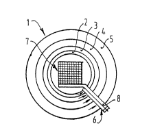
A first embodiment l of a radiation-sensitive means
according to the present invention comprises four rings 2,
3, 4 and 5 wherein charge generated by radiation in radiati-
30 on-sensitive elements is carried via transfer elements
coupled to these radiation-sensitive elements to a drain
means 6 consisting of drain elements for radial draining of
this charge. In the centre is a rectangular charge-coupled
device 7 of per se known type provided with a drain means 8.
As stated above, the embodiment shown in fig. l has
advantages for use in robotics as the radial change of the
density or resolution of radiation-sensitive elements here
WO90/13915 PCT/EP90/00818
3 ~32~
forms an approximation of the resolution of radiation-sensi-
tive elements occurring in the human eye.
These advantages likewise obtain for the embodiment shown
in fig. 2, wherein the signals deriving from radiation-
5 sensitive elements are transferred according to the arrows
radially outward in sections 9, ].1, 12 to an annular drain
means 13 provided with an output connection 14. Disposed in
the centre is a rectangular or square CCD 16 provided with a
radial drain means 17.
The radiation-sensitive means 18 (fig. 3) according to r
the invention comprises a middle section 19, an inner ring
20, a central ring 21, an outer ring 22 and a radial drain
means 23 wherein the signals transported in the direction of
the arrows of both the central section 19 and the circular
15 registers ar~ combined.
With the embodiment 18 of fig. 3 of the radiation-sensi-
tive means, operation is carried out with a basic element of
standard design of a radiation-sensitive element having a
transfer element coupled thereto. The basic elements of four
20 radiation-sensitive elements and transfer elements coupled
thereto are designed per ring 20, 21 and 22 using CAD tech-
niques and the dimensions of guch cells become greater in a
ring in outward direction, while in a following ring they
are smaller on the inner side thereof than on the outside of
25 the preceding ring in outward direction.
A detail of the embodiment 18 of fig. 3 comprises four
light-sensitive regions 26-29 arranged on a p-type silicon
substrate 31 wherein a thin layer of n+Si 32 is applied,
over which an oxide layer 33 is arranged (fig. 4, 5). Arran-
30 ged on the oxide layer 33 are regions 34, 36, 37, 38, 39 ofvarying conductivity of polysilicon. In addition a region 41
of polysilicon is applied close to each of the light-sensi-
tive regions 26-29. Applied over the polysilicon layers is a
thick oxide layer 42 whereover is arranged a light-screening
35 layer 43, for instance of aluminium.
The polysilicon regions 34-39 are subject to three-phase
control, as known in CCD techniques. Conducting paths 44,
WO90/1391~ PCT/EP90/00~18
2 ~ 3 ~ ~ 2 ~
45, 46 and 47 which can be connected to the layers of poly-
silicon are only indicated schematically. The aluminium
layer 43 is interrupted at the light-sensitive region 29
whereby electron-hole pairs are generated in the layers 31
5 and 32 thereunder. Via the region 41 these charge carriers
are sent to below a layer 38, whereafter the charge carriers
are transported in parallel to the radial drain means 23.
The charge carriers shifted along the circle are carried
into the radial drain means 23 using a coupling element 51
lO shown schematically in fig. 6. After an electrode 52 (fig.
7A, 7C, wherein negative voltage levels are indicated in
upward direction) has obtained a high value after the situ-
ation drawn in fig. 7B, the charye carriers are collected in
a potential well 54 beneath a relevant electrode of a circu-
15 lar shift register. In order to apply a negative voltage toelectrode 53 (fig. 7B) tc a level beyond a level on an
electrode 55 (fig. 6) the charge carriers are carried into
the potential well 56 distributed evenly between electrode
55 and an electrode 57 of the radial drain means. By apply-
20 ing a negative voltage to electrode 58 (fig. 7E) the poten-
tial well 56 is divided into two parts 59, 61, whereafter
the charge carriers in the part of the well 59 can be drai-
ned using an electrode 62 (fig. 7E, 7F), wherein level 63
indicates the voltage level on the electrode 62. By increa-
25 sing the voltage above the potential well 61 the charge issubsequently carried over potential barrier 64 into the
potential well 65, after which it can be clocked through,
for instance at a frequency of 1 MHz in radial direction,
wherein the cycle can repeat itself in fig. 7I.
Selecting the ratio between the size of the regions 66
and 67 in fig. 6 determines the portion of the charge car-
riers that reaches the radill drain means 23 of fig. 3. The
ratio between the regions 66 and 67 will therefore differ in
different rings of the radiation-sensitive sensor.
The central portion 19 of the preferred embodiment 18 of
fig. 3 preferably comprises radiation-sensitive elements 71
that are coupled to rectilinear registers 72 which are in
.
':' -
~:: , .
.... . -~: .
.. ~; . , !
~ WO90~13915 PCT/EP90/00818
2n32~2~
turn coupled to registers 73 extending at right angles
thereto which converge to the radial drain means 23. The
radiation-sensitive elements are in preference each arranged
staggered in the direction parall~el to the drain means 23.
.: ... ..
,