Note: Descriptions are shown in the official language in which they were submitted.
fi60
LINE INTERFACE CIRCUIT
Field of the Invention
The invention relates to telecommunications and
more particularly relates to a line interface circuit for
supplying energizing current for operating a telephone
station set and for coupling signals between a telephone
facility and the telephone set vla a two wire communication
line.
Backqround of the Invention
Over the past decade in many countries, operating
telephone companies have been investing extensively in a new
generation of telephone switching equipment, generally
referred to as digital switching systems. Such systems are
characterized by an abundance of silicon based integrated
circuits which act in concert to provide time division
multiplex channels for coupling telephone sets in
communication as required. Such systems are attractive
because they require less space, less maintenance and
attract greater revenue as compared to previous systems which
provided for communications via metallic paths. Substantial
design efforts have been committed to developing appropriate
line interface circuits in the same technology. Recently
transformerless analog silicon based integrated line
interface circuits which are capable of performing coupling
requirements between a switching system and a telephone set
have become available. However many of the transformerless
line circuit designs require a degree of precision and
perfection in manufacturing, which typical state of the art
integrated circuit manufacturers find difficult and expensive
to meet. For example in United States Patent No. 4,514,595,
an "Active Impedance Line Feed Circuit", S.D. Rosenbaum et
al disclose tip and ring amplifiers which are intended to
feed tip and ring leads of a telephone line with the
preferred direct current feed resistance of 400 ohms and the
preferred AC impedance of 900 ohms. A control circuit
drives the amplifiers in differential response to signals
2~
derived across matched tip and ring feed resistors which are
coupled in series with outputs of the tip and ring
amplifiers. The derived signals are coupled to a
differential input of the control circuit via precision tip
and ring voltage dividers. It is recommended that 0.05%
tolerance feed resistors and 0.1% tolerance voltaye divider
resistors are preferred for interfacing telephone lines with
a central switching office. Furthermore it is recommended
that the differential input have the best possible common
mode rejection characteristic so that longitudinally induced
signals on the telephone line can be tolerated. Consequently
the spectacular price and performance advantages realized in
silicon based central office switching networks were not
achieved to similar degree by this design of a line feed
circuit.
In many switching systems, an individual line
circuit is required to interface to each and every telephone
line that is connected to the switching system. Hence, the
cost of the line interface requirement has continued to be a
major portion of the hardware cost of such switching systems.
Furthermore in association with many telephone lines, the
price/operating performance of many typical transformerless
line interface circuits is often inferior to that of older
designs as exemplified in United States Patent No. 4,103,112
issued to V.V. Korsky on July 25, 1978. This is often due to
the conditions in which a particular telephone line is
required to operate. For example excessive longitudinal
energy may be reactively coupled to the telephone line from
nearby power utility distribution lines. Longitudinally
induced currents on longer telephone lines may exceed the
direct energizing current while the telephone set is in the
OFF HOOK condition. This results in periodic reversals in
the flow of the energizing current. In his United States
Patent No. 4,484,032, "Active Impedance Transformer Assisted
Line Feed Circuit", S.D. Rosenbaum recognized some of the
difficulties associated with his transformerless design and
reintroduces a transformer. In this later development, his
original design is modified in that feed resistor and
fi6~3
voltage divider resistor recommended tolerances are loosened
to 1% by using only the direct current component of the
signals derived across the tip and ring feed resistors while
differential AC signals are transformer coupled to the
differential amplifier, substantially to the exclusion of
longitudinal AC signals. However the tip and ring
amplifiers are yet required to tolerate longitudinal currents
on the telephone line. As the feed resistor may also be
exposed to severe electrical stress, as can be the result of
a random transient event such as a lightening strike or a
power line cross, the values of the feed resistors may become
altered beyond tolerance limits for acceptable line circuit
operation.
It is an object of the invention to provide a line
interface circuit wherein common mode signals are
substantially impeded such that required common mode
rejection characteristics of active components in the circuit
are less critical.
Summary of the Invention
In a line interface circuit, tip and ring feed
amplifiers are sufficiently isolated from longitudinal
signals, as may be reactively impressed upon a telephone
line, that unidirectionally conductive amplifying devices are
sufficient to provide for the tip and ring feed amplifier
functions.
In accordance with the invention alternating
current signals are differentially coupled between a two wire
communications line and a telecommunications facility by
differentially driving signals destined for the two wire
communications line, with a predetermined source impedance,
via tip and ring amplifiers and tip and ring feed resistors;
differentially receiving, by means of a differential
amplifier, signal voltages being developed by currents
traversing the tip and ring feed resistors; detecting
signals destined for the telecommunications facility by
subtracting a representation of the signals destined for the
two wire communications from a representation of the
~t~32~
differentially received signals; and notch filtering, in
series with the tip and ring feed resistors, to impede any
longitudinal signals of about a predetermined frequency which
would otherwise traverse the tip and ring feed resistors,
whereby a routinely available industry standard common mode
rejection performance characteristic of said differential
amplifier consistently yields telephony standard performance
in the presence of reactively coupled longitudinal power line
frequency signals.
A line interface circuit in accordance with the
invention provides for coupling differential alternating
current signals between a telephone facility and tip and ring
leads of a two wire communications line, to the substantial
exclusion of longitudinal signals of about a predetermined
frequency. The line interface circuit includes tip and ring
amplifiers each having an output, and an input for receiving
alternating current signals destined for the communications
line and tip and ring terminals for connection to the tip and
ring leads respectively. A transformer includes a secondary
winding having an inductance, and tip and ring windings
being similar with respect to each other. The tip winding is
connected in series between the tip terminal and the output
of the tip amplifier, and the ring winding is connected in
series between the ring terminal and the output of the ring
2S amplifier. The tip and ring windings are arranged in flux
reinforcing configuration with respect to any longitudinal
signal current at the tip and ring terminals. A reactive
element is connected across the secondary winding for
providing a series resonant circuit having a resonant
frequency of about said predetermined frequency, whereby
longitudinal signals of about said resonant frequency are
impeded.
In one example in accordance with the invention the
line interface circuit comprises:
tip and ring amplifiers each having an output, an
input for receiving alternating current signals destined for
the communications line, a transistor having an emitter
electrode, a base electrode, and a collector electrode, the
~o~
collector electrode corresponding to said amplifier output, a
first resistor being connected between a respective one of
the power terminals and the emitter electrode, a second
resistor being connected be~ween a respective one of the
power terminals and the base electrocle, an AC coupling
network being connected between the input terminal and the
base electrode, a DC feedback path being connected between
the output terminal and the base electrode, and an AC
feedback path being connected between the output terminal and0 the base electrode;
tip and ring terminals for connection to the tip
and ring leads respectively;
a transformer including a secondary winding, having
an inductance, and tip and ring windings being similar with
respect to each other, the tip winding being connected in
series between the tip terminal and the output of the tip
amplifier, and the ring winding being connected in series
between the ring terminal and the output of the ring
amplifier, the tip and ring windings being arranged in flux
reinforcing configuration with respect to any longitudinal
signal current at the tip and ring terminals;
a reactive element being connected across the
secondary winding for providing a series resonant circuit
having a resonant frequency of about said predetermined
frequency, whereby longitudinal signals of about said
resonant frequency are impeded;
a resistance network including tip and ring feed
resistors and tip and ring voltage taps being defined by tip
and ring voltage dividers connected across the tip and ring
feed resistors, the tip feed resistor being connected between
the tip terminal and the output of the tip amplifier, in
series with the tip winding, and the ring feed resistor being
connected between the ring terminal and the output of the
ring amplifier, in series with the ring winding; and
an amplifier circuit having a transmit output and
being responsive to differential signals across the tip and
ring voltage taps and to AC signals at one of the inputs of
the tip and ring amplifiers for providing AC signals from
2~3~
the communlcations line and destined for the telephone
facility at the transmit output.
Brief Description_of the Drawinqs
An example embodiment is discussed with reference
to the accompanying drawings in which:
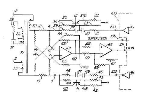
Figure 1 is a schematic diagram of a line interface
circuit in accordance with the invention; and
Figure 2 is a graphical representation of a
functional characteristic of a filter used in the line
interface circuit illustrated in figure 1. The graph
includes a horizontal axis graduated in kilohertz and a
vertical axis graduated in decibels.
Description of the Example Embodiment
A typical telephone line interface circuit is
intended for use for coupling alternating current (AC)
signals between a two wire telecommunications line,
frequently referred to as a subscriber loop, and a telephone
switching facility, typicall~ a central office, or a remote
line module or concentrator associated with the central
office. The line interface circuit is also intended to
supply the two wire telecommunications line with energizing
direct coupled (DC) current, such that a telephone set or
the like being connected to the line will be supplied with at
least about twenty milliamperes of DC current while it is in
an OFF HOOK state.
The line interface circuit in figure 1 includes a
tip terminal 2 and a ring terminal 3, for connection to tip
and ring leads of a subscriber loop, not shown. An input
terminal 102 of a tip amplifier 20, and an input terminal 103
of a ring amplifier 40, are connected to receive AC signals
which are destined for the subscriber loop, from an access
circuit 100, which is associated with a telephone switching
facility, not shown. AC signals from the subscriber loop
and destined for the telephone switching facility are coupled
to the access circuit 100 via a terminal 101. Supervision
signal which indicate ON HOOK, OFF HOOK and DIAL information
~C~3~
to the access circuit 100 are communicated thereto via a
terminal 106. Power terminals, labeled +V and -V, are for
connection across corresponding terminals of a central office
battery supply, not shown, usually a -48 volt supply. In
this example a reference voltage of about -24 volts,
convenient for the operation of an amplifier circuit 60, is
supplied via a voltage reference lead V Ref.
In the line interface circuit, the tip amplifier 20
includes a PNP transistor 21 being connected via collector,
emitter and base electrodes in combination with resistors 22-
26 and capacitors 27 and 28 between the power terminal +V,
the terminal 4, and the input terminal 102, as shown. The
ring amplifier 40 includes an NPN transistor 41 being
connected via collector, emitter and base electrodes in
combination with resistors 42-46 and capacitors 47 and 48,
between the power terminal -V, the terminal 5, and the input
terminal 103, as shown.
A resistor network 10 includes a tip feed resistor
12 connected in series with the collector electrode of the
PNP transistor 21 via the terminal 4, and a ring feed
resistor 13 connected in series with the collector electrode
NPN transistor 41 via terminal 5. The resistor network 10
also includes tip and ring voltage dividers 14 and 15
connected as shown to provide tip and ring voltage taps 6
and 7.
A transformer 30 includes a tip winding 32
connected in series between the tip feed resistor 12 and the
tip terminal 2, and a ring winding 33 connected in series
between the rinq feed resistor 13 and the ring terminal 3.
The tip winding 32 and the ring winding 33 are poled in such
a way that differential mode currents are of a flux
cancelling effect, while common mode currents, as may result
from electrical energy being induced longitudinally along the
subscriber loop, are of a flux adding effect in the
transformer 30. The transformer 30 also includes a secondary
winding 35 across which a capacitor 37 is connected in series
with a resistor 38 to provide a notch filter 35. The value
of the capacitor 37 is preferably chosen so that in
~:~32~
combination with inductance of the secondary winding 36, the
notch filter 35 exhiblts a characteristic generally as
exemplified in figure 2, for significantly impeding traversal
of the tip winding 32 and the ring winding 33 by common mode
currents at utility power line frequencies. Component values
and parameters in relation to the transformer 30 and the
notch filter 35 are as follows:
windings 32, 33 - 700 turns (.54H) each
winding 36 - 2500 turns (6.9H)
capacitor 37 - 1 microfarad
resistor 38 - 1 kilohm
The amplifier circuit 60 includes a first amplifier
61 having a differential input and an output and being
connected in combination with resistors 62-64, the tip
voltage tap 6, the ring voltage tap 7, and the voltage
reference lead V Ref. A second amplifier 65 has a
differential input and an output connected in combination
with resistors 66-69, and the terminal 101.
In operation, the energizing DC current flow is
via the PNP transistor 21 and the NPN transistor 41 which are
operated to each have a collector electrode source resistance
of about 100 ohms. The source resistance is determined by
chosen values of the resistors 22-24 and 42-44 respectively.
The tip feed resistor 12 and the ring feed resistor 13 are
also chosen preferable to each be within 5% of 100 ohms
whereby the overall source resistance is about 400 ohms, in
this example. The AC source impedances at the collector
electrodes of the PNP transistor 21 and the NPN transistor 41
are primarily determined by the chosen of values the
components 25-28 in relation to the resistor 22, and by the
chosen values, the components 45-48 in relation to the
resistor 42, respectively. Component values and parameters
in relation to the tip amplifier 20 and the ring amplifier 40
are as follows to provide a source impedance substantially
equivalent to 900 ohms in series with 2.16 microfarads across
the tip terminal 2 and the ring terminal 3:
resistor 22 - 22 ohms
resistor 23 - 33 kilohms
~3~
resistor 24 - 100 kilohms
resistor 25 - 10 kilohms
resistor 26 - 9.1 kilohms
capacitor 27 - 0.1 microfarad
capacitor 28 - 0.1 microfarad
resistor 42 - 20 ohms
resistor 43 - 33 kilohms
resistor 44 - 100 kilohms
resistor 45 - 10 kilohms
resistor 46 - 9.1 kilohms
capacitor 47 - 0.1 microfarads
capacitor 48 - 0.1 microfarads
The tip amplifier 20 and the ring amplifier 40 respond to AC
signals applied at the input terminal lC2 and the input
terminal 103 to differentially drive the subscriber loop via
the tip terminal 2 and the ring terminal 3.
When the telephone instrument associated with the
subscriber loop is in an OFF HOOX condition, differential
currents traversing the tip feed resistor 12 and the ring
feed resistor 13 are the result of AC signals from the tip
amplifier 20 and the ring amplifier 40, in addition to
modulation of the energizing direct current effected by the
telephone instrument. These currents develop corresponding
voltage signals across the tip feed resistor 12 and the ring
feed resistor 13 which are coupled to the amplifier circuit
60 via the tip voltage tap 6 and the ring voltaye tap 7. The
first amplifier 61 amplifies these voltage signals and
provides corresponding signals for use in a supervision
detection function performed by way of the access circuit
100, and for use by the second amplifier 65 for detection
and transmission of AC signals destined for the telephone
switching facility via the terminal 106.
As previously mentioned, tolerances for ohmic
values of the tip and ring feed resistors and the resistors
in the tip and ring voltage dividers are substantially
relaxed to about 5%, as compared with tolerances which were
preferably restricted to 1% or less, for similar circuit
elements in previous line interface circuits. Of course this
~03~fi60
relaxation of ohmic tolerances bring~s with it a small but
significant reduction in manufacturing cost and an increased
probability of long term acceptable circuit functionality.
These advantages accrue from the arrangement of the
transformer coupled notch filter in series with the resistor
network 10. Similarly, the common mode rejection
characteristic of the differential input of the amplifier
circuit 60 is likewise relaxed. Hence it is envisaged that
further economic advantage may be derived by integrating the
amplifier circuit 60 into a substrate common to the access
circuit lO0. In such an arrangement the terminals 101 and
106 migrate to the interior of the access circuit lO0,
becoming effectively nonexlstent, and the voltage taps 6 and
7 are connected at corresponding new terminals of the access
circuit 100. The resistor network 10 and the tip and ring
amplifiers 20 and 40 would most likely remain as being
provided by discrete components as these may from time to
time be exposed to extraordinary electrical stresses that
would likely be damaging to the typical silicon integrated
circuit.