Note: Descriptions are shown in the official language in which they were submitted.
~ -- 203273~
PHASE Dl~K~NCE CONTROL CIRCUIT
FOR INDUCTION FURNACE POWER SUPPLY
Field of the Invention
This invention relates to apparatus and method for
controlling the power in an induction coil in an induction
furnace. The invention varies the phase shift between load
voltage and current, thus varying the apparent impedance of
the load. The present invention further includes means for
reducing power to the load in certain situations.
Back~ d of the Invention
Induction heating is a method of melting or other-
wise heating a quantity of metal, not by applying heat
externally, but by using the metal workpiece as its own
heat source. An induction melting furnace generally
includes a container for holding metal to be melted, an
induction coil surrounding the container, and a power
supply having an output circuit connected across the coil.
In operation, the power supply creates current flow through
the coil which, in turn, causes an alternating magnetic
field to pass through the metal within the container.
This field induces current flow in the metal so that the
metal is heated internally by resistance heating.
946-186(CIP)l.CN -1-
/lp/#11
2032732
In its electrical characteristics, an induction
furnace is often visualized as equivalent to a transformer
with a primary coil and a melt charge which behaves like a
shorted secondary coil. The power released into the melt
charge is proportional to the square of the current in the
induction coil (primary coil):
p =Imelt R
where:
P = power;
Imelt = current in the melt bath; and
R = resistance of the melt.
Further, the current induced within the melt charge
is equal to the current in the primary coil times the
number of turns in the coil, or:
Imelt = nICoi
where:
n = number of coil turns;
Icoil = current in the coil;
therefore
P = n2Icoil2R
Since melt charges are almost always of metals
having low resistance, providing high power to the melt
charge requires either a high number of turns or a high
current in the induction coil. These, in turn, yield poor
efficiencies. Induction coils usually have low power
factors.
To offset high inductance of the coil, it is usual
to include a capacitor in the circuit, creating an RLC
oscillating circuit. As is well known in the art, the
amplitude of an alternating current in an RLC circuit can
946-186(CIP)l.CN -2-
/lp/#ll
2032732
be controlled by varying the frequency of the current. A
given RLC circuit will have a resonant frequency, at which
the current amplitude will reach a maximum value. From an
efficiency standpoint, to operate an induction furnace at
its resonant frequency will maximize the energy transferred
into the melt charge. However, to operate an induction
furnace at its resonant frequency is impractical, as will
be explained in detail below.
Figure 1 is a block diagram of a typical induction
furnace. External power is provided from a commercial
source, and is usually in the form of 60 Hz AC from the
power mains. The 60 Hz AC is rectified to provide high
voltage DC. The DC is fed into an inverter 10, which
usually utilizes silicon controlled rectifiers (SCRs) to
"chop" the DC voltage into a square wave shape. The
frequency of the "chopping" is determined by the frequency
of the SCR firing. The speed at which the SCRs are fired
thus controls the frequency of the resulting square wave.
The square wave is then fed into the RLC circuit, in which
the melt charge and induction coil may be regarded as a
core disposed within an inductor L. As is well known,
when alternating voltage is fed into an RLC circuit, a
current having a sine-wave shape flows in the RLC circuit.
The frequency of the voltage square wave and the resulting
current sine-wave is directly controlled by the frequency
of the SCR firing.
Figure 2 shows a typical type of inverter (such as
the inverter shown in Figure 1), a "full-bridge" inverter
10, connected between a DC source 12 and the RLC circuit
14. (The n2R term at 14 represents the equivalent resis-
tance of the RLC circuit, taking into account the number of
turns n in the coil and the resistance R of the melt.) The
full-bridge inverter 10 comprises four diodes 16 as shown,
and four SCRs which operate in pairs 18a, 18b, and 2Oa,
2Ob, respectively. The SCRs operate as switches which
complete a circuit when they are "fired" (i.e., rendered
946-186(CIP)l.CN -3-
/lp/#ll
~03273~
conductive) by an external control signal. In a full-
bridge inverter, the SCRs 18a, 18b and 20a, 20b are turned
on and off alternately in pairs at the desired frequency
for the square wave. The arrows in Figure 2 show the
direction of current from the DC source 12 when SCRs 18a,
18b are fired and SCRs 20a, 20b are left open (i.e, non-
conductive). SCRs 18a, 18b complete a circuit from which
DC from source 12 flows through the RLC from left to right,
as can be seen by the arrows. If, alternatively, SCRs 18a
and 18b are in a non-conductive state, and SCRs 20a and
20b are fired, current will flow in the opposite direction
through RLC 14, from right to left. As those skilled in
the art will understand, an SCR, once fired, will conduct
electric current as long as this current flows from the
SCR's anode terminal to the cathode terminal. Should the
current change direction, the SCR will block conduction and
after a short period, usually 30-70 ~sec, will turn off and
again become non-conductive. This period is called "turn-
off-time" or TOT, for short.
Figure 3 shows a series of curves graphically des-
cribing the behavior of the current of Figure 2 in the
course of one and a half cycles of the inverter 10. With
reference to curve 100, which describes the current asso-
ciated with the inverter over time, and curve 110, which
describes the power associated with the inverter over time,
the action of inverter 10 can be summarized thus:
At to: One set of SCRs is fired. Positive
current delivered to RLC, resulting in positive
power dissipation in the load.
At tl: Sine-curve behavior of RLC causes
inverter current to become zero and then negative
(shaded area lOla). Because current is negative
while voltage is still positive, power to RLC
becomes negative (shaded area llla). This repre-
sents power not dissipated by the load. Reversal
946-186(CIP)l.CN -4-
/lp/#ll
203273~
of current through first set of SCRs causes them to
shut off.
At t2: Alternate set of SCRs is fired,
causing reversal of direction of voltage across the
RLC. Because current and voltage are now both of
the same polarity, power is again dissipated in
the load.
At t3: Inverter current crosses zero point
and becomes positive (shaded area lOlb). Because
current is positive and voltage is negative, no
power is dissipated (shaded area lllb).
At t4: First set of SCRs is again fired.
Current, voltage, and power are all positive and
the cycle begins again.
The above summary will now be explained in detail.
When DC is input into an RLC circuit, the circuit
will "ring", and oscillations of voltage and current will
result. The frequency of these oscillations depends on the
specific values of the RLC components, including the prop-
erties of the melt charge inside the inductor. When SCR
pair 18a, 18b is fired, current flows through the RLC
circuit and the inverter in the direction of the arrows
(Figure 2). Current will gradually build up to its maximum
value and then subside to zero, as illustrated in curve 100
of Figure 3. The total energy passed from the DC source to
the melt charge during the interval to ~ t1, half a period
for the oscillation of the RLC circuit, is:
E = to~tl vi dt > 0 (1)
where v and i are voltage and current in the RLC circuit,
respectively.
During this half-cycle, charge accumulates on the
capacitor. At time t1, the voltage on the capacitor is
larger than the DC voltage and the capacitor begins to
discharge, reversing the direction of the current along
946-186(CIP)l.CN -5-
/lp/#11
2032732
the path given by the arrows in Figure 2. This reversal of
current will cause SCRs 18a, 18b to turn off. After the
turn-off-time (TOT) of SCRs 18a, 18b, this pair of SCRs
will become non-conductive (although current can still
return to the DC source through the diodes 16). For the
period between tl, when the capacitor begins to discharge,
and t2, when the other set of SCRs 20a, 20b is fired, the
extra energy stored in the capacitor is returned to the DC
source. The energy returned to the DC source between t
and t2 is given by:
E = t1~t2 v(-i)dt < 0 (2)
This reversal of current is illustrated in curve 100 of
Figure 3 as the negative portion of the curve between t
and t2, encompassing shaded area 101a.
Normally, in a full-bridge inverter and many other
types of inverter, the other pair of SCRs will be fired at
some time after the turn-off-time of one pair of SCRs.
When the other pair of SCRs 20a, 20b are fired, the DC from
the source 12 flows through the RLC from right to left in
Figure 2, and the capacitor, begins to charge to the
opposite polarity. Between points t2 and t3 in curve 100
in Figure 2, the voltage and current relative to the DC
source have the same polarity and therefore the energy
transferred to the load is positive:
E = t2rt3 (-v)(-i)dt > 0 (3)
In summary, energy is passed from the DC source to
the metal charge (via the coil) when the voltage and
current have the same polarity. This condition exists, in
curve 100, between to and tl and between t2 and t3. During
the period tl to t2, and between t3 and t4, energy is not
being passed to the coil but is being returned to the DC
source. These periods of negative energy are shown as
946-186(CIP)l.CN -6-
/lp/#11
20~2~32
shaded areas 101a and 101b in curve 100 and llla and lllb
in curve 110. Over the period T of an operating cycle
(from to to t4), the power produced by the inverter can be
determined as:
P = 1 to~t4VI dt (4)
T
Assuming that the current is a sine wave and the
voltage a square wave, as would be the case with such an
inverter, the power passed from the inverter to the furnace
will be equal to:
P = 2 VIcos~ (5)
7r
where:
V - inverter voltage (=VDc for a full-bridge
inverter);
I - amplitude of inverter current;
f - frequency of SCR firing (l/T)
= 2t
T - phase shift between voltage and current;
t - time interval in which energy is being returned
to the DC source.
The key to equation (5) is the relationship of the
phase difference ~ and the time interval t within each
cycle in which energy is being returned to the DC source.
From Figure 3, it can be seen that for every cycle of
inverter current (to to t4), there are two periods of equal
duration in which power is returned to the source. These
periods are the same as the periods between the zero
crossing of the current and the zero crossing of the
voltage in the inverter, which can be seen by a comparison
of the zero crossings of curve 100 and curve 108. It is
clear from equation (5) that, for ~ between 0 and 90, an
increase in ~ will cause a decrease in power. Thus, as
946-186(CIP)l.CN -7-
/lp/#ll
2032732
increases, power passed to the furnace decreases. Maximum
power transfer occurs when ~=0.
However, a dangerous condition exists in an RLC
circuit at resonance, in which ~1 equals ~O. Resonance is
the point of maximum power transfer, when there is zero
phase shift between voltage and current in the inverter.
Zero phase shift means, in effect, that one set of SCRs is
being turned on at exactly the same instant the other set
is being turned off. This would be no problem if SCRs
behaved as idealized switches, which open instantly.
However, there is a finite period of time, the turn-off
time (TOT) during which an SCR is still conductive after
being turned off. If the phase shift is less than the TOT
of the SCRs, all of the SCRs will be conductive at the same
time, thus causing a short across the DC source. Thus, in
order to avoid shorting out the power supply, the phase
shift between voltage and current must always be greater
than the TOT of the SCRs. This amounts to the same thing
as preventing the frequency of the DC chopping from approa-
ching the resonant frequency of the RLC. In order tooperate safely, the frequency of SCR firing must always be
safely below the resonant frequency of the RLC.
The engineering problem posed by this requirement
is that the resonant frequency of an induction furnace does
not remain constant but may vary considerably in the course
of use. The physical properties of the melt charge, which
acts as the inductor core, have a direct and significant
effect on the resonant frequency of the furnace. These
significant physical properties include the temperature of
the melt charge at any given point of the heating opera-
tion, the amount of metal in the furnace at any given time,
and the specific composition of the alloy being heated.
These properties will vary widely with every situation, and
even within the course of a single use of the furnace. It
is not uncommon in induction melting to add cold metal to
the furnace while a previously added batch is still heat-
946-186(CIP)l.CN -8-
/lp/#11
2032732
ing, thus changing the mass, temperature, and crystal
structure of the core almost instantaneously, and thereby
almost instantaneously changing the resonant frequency of
the inductor.
Of course, the SCR firing frequency could be kept
extremely low so that the phase shift will always be
greater than TOT, even at resonance. This approach is
unacceptable because the power supply would become extreme-
ly inefficient. Because it is crucial that the input
frequency be less than the resonant frequency, and because
the resonant frequency may change so suddenly, a control
system to control SCR firing frequency in response to new
physical conditions in the furnace is required so that
phase shift may be minimized for high efficiency yet never
less than TOT to avoid shorting the power supply.
It is also theoretically possible to calculate the
resonant frequency of an induction furnace at any given
instant, given the instantaneous temperature, the mass of
the core, and physical properties of the core, and thereby
change SCR firing frequency as required but as a practical
matter these parameters are too difficult to measure, and
are not suitable as inputs to a control system.
One common attempt at solution to this problem is
varying the inverter frequency electronically, using
voltage-controlled oscillators. The voltage-controlled
oscillators generate pulses with a frequency proportional
to a control voltage produced by a closed-loop circuit
which measures the output power and compares it with a
preset desired value. However, this method has a major
drawback in that a frequency control system generally
cannot adapt to sudden changes in electromagnetic proper-
ties of the furnace. If a cold charge is dropped into the
melt, the system is likely to encounter the new resonant
frequency before the frequency can change, and the inverter
will crash. Special protection circuits to detect such a
condition are cumbersome and do not work well.
946-186(CIP)l.CN -9-
/lp/#11
2032732
In contrast, the present invention controls power
delivered to the induction coil by varying the phase
difference between current and voltage in the coil in
response to the resonant frequency of the load. The
present invention does not directly vary the frequency of
the inverter AC voltage. Instead, the present invention
monitors the zero-crossings of the current in the inductor,
and adjusts the time delay before the SCR's are fired in
such a way that the output power level is maintained and
that there will always be at least a minimum phase shift ~
between current and voltage. Although the frequency of the
DC voltage may vary in the course of use of this method it
is important to understand that the method merely reacts to
the resonant frequency in the RLC load circuit under a
variety of conditions.
SummarY of the Invention
The present invention is a method and apparatus for
controlling the power supplied to an induction furnace by
an inverter power supply having switch means for generating
an alternating polarity voltage across the load. The zero-
crossings of the current in the furnace is monitored and
the polarity of the voltage through the load is changed
after a delay interval following the zero-crossing of the
current. The duration of the delay interval is determined
by a preselected power level associated with the furnace,
and the turn-off-time characteristics of the switch means
within the power supply.
In a preferred embodiment of the invention, the
duration of the delay interval is affected also by a number
of other parameters, such as currents to the furnace in
excess of a preselected maximum, voltage across the capaci-
tor of the RLC in excess of a preselected maximum, and
frequency of the current in the RLC in excess of a pre-
selected maximum.
946-186(CIP)l.CN -10-
/lp/#ll
203273~
The control system of the invention includes
automatic control with a manual override for emergency
situations. The system includes means for monitoring the
power delivered to the load and means for varying the power
delivered to the induction load by controlling the phase
difference between voltage and current delivered to the
load. Feedback means automatically control the phase
difference between voltage and current in response to the
measured power delivered to the load. Means are further
provided for introducing an external signal into the
feedback means, whereby the external signal supersedes the
automatic controlling of the power delivered to the load.
Brief Description of the Drawings
For the purpose of illustrating the invention,
there is shown in the drawings a form which is presently
preferred; it being understood, however, that this inven-
tion is not limited to the precise arrangements and instru-
mentalities shown.
Figure 1 is a simplified schematic diagram showing
the general layout of the power supply for an induction
heater according to the prior art.
Figure 2 is a schematic diagram of a full-bridge
inverter between a DC source and an RLC load, according to
the prior art.
Figure 3 is a series of waveforms present at
various points in the control system of the present inven-
tion.
Figure 4 is a simplified block diagram showing the
basic elements of the present invention.
Figure 5 is a simplified block diagram showing one
embodiment of the present invention.
Figure 6 is a block diagram showing the elements
of the invention shown in Figure 4 in greater detail.
Figure 7 is a simplified cross-sectional view of an
induction furnace having liquid metal therein.
946-186(CIP)l.CN -11-
/lp/#ll
2û3273~
Figure 8 is a simplified block diagram showing the
basic elements of an embodiment of the present invention
having a safety feature.
Figure 9 is a schematic circuit diagram showing the
preferred embodiment of the safety feature of the present
invention.
Detailed Description of the Invention
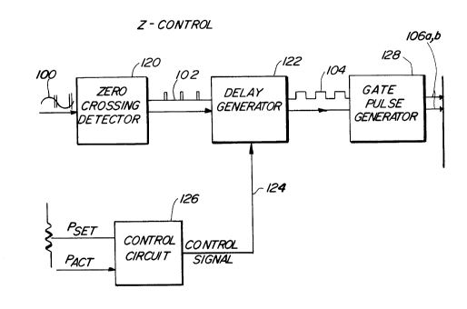
Figure 4 is a block diagram showing the basic
elements of the invention. These elements may be embodied
electronically in any form, such as by analog circuit,
digital circuit, or microprocessor. An analog embodiment
of the present invention is described below. Figure 4,
together with the waveforms of Figure 3, illustrate the
general principles by which the control system of the
present invention controls power passing from the power
supply to the melt charge.
Curve 100 in Figure 3 represents the behavior of
the current in the RLC load in response to the square-wave
voltage. A first set of SCRs, as in figure 2, is fired at
to. When there is a flow of energy into the RLC load, as
between points to and tl, voltage accumulates on the
capacitor and power is transferred from the power supply
to the melt charge. At point t1, following the natural
sinusoidal behavior of current in an RLC, the current
crosses a zero point and becomes negative (i.e., changes
direction), as seen in the shaded area marked 101. A
negative current flow causes the SCRs to turn off. During
the turn-off period and before firing of the other set of
SCRs, energy will be flowing back to the DC source instead
of passing to the melt charge.
The point of zero crossing of the current in the
RLC is thus important because the zero crossing marks the
point at which energy begins flowing back to the DC source.
Energy will flow back to the source until the SCRs turn
off. Once the SCRs have turned off, the other set of SCRs
946-186(CIP)l.CN -12-
/lp/#ll
2032732
may safely be turned on. By turning on the other set of
SCRs immediately after the first set has turned off,
efficiency is maximized while preventing a short circuit.
The current in the RLC is monitored by a zero-
crossing detector, shown as box 120 in Figure 4, whichgenerates a strobe pulse at every zero crossing of the
current in the RLC. This strobe pulse is shown as waveform
102 in Figures 3 and 4. As can be seen in Figure 3, each
strobe is synchronous with the zero-crossing of curve 100.
Zero-crossing strobe pulses 102 are then fed into a
delay generator 122. Delay generator 122 produces a square
pulse of a fixed duration in response to each incoming
strobe pulse 102, as shown by waveform 104. This duration
may be varied by a control signal 124.
Control signal 124 is produced by control circuit
126 in response to a difference signal, which is preferably
but need not be related to the power associated with the
RLC. Any parameter relevant to the particular job, such as
voltage or frequency, may also be used as the control
parameter. Considering power as the relevant parameter to
be controlled, the control circuit includes means for
comparing the actual measured power in the RLC at a given
time with a value preset by the operator. Typically, the
preset power value will be chosen so as to prevent the
power in the RLC from exceeding a safe level. The control
circuit 126 produces a difference signal related to the
instantaneous difference between power associated with the
RLC and the preset value, and this difference signal is
used to operate the control signal 124 sent to the delay
generator 122.
Generally if actual power detected in the RLC
exceeds a preset value, the control signal causes the delay
generator to increase the duration of each square pulse in
waveform 104, causing an increase in the time between the
zero crossing of current in the RLC and the firing of the
other set of SCRs. An increase in this period means an
946-186(CIP)l.CN -13-
/lp/#ll
203~732
increase in the time within each cycle during which energy
is flowing back to the DC source, and therefore reducing
the total amount of power passing to the melt charge within
each cycle.
The output of the delay generator is sent to a gate
pulse generator 128. Gate pulse generator 128 fires the
appropriate pair of SCRs in response to the trailing edge
of each square pulse of waveform 104. Because gate pulse
generator 128 fires the pairs of SCRs in the bridge alter-
nately, the firing pulses shown as waveform 106 in Figure 3
are split so that every other pulse appears on one of two
lines. Waveform 106a, for example, would fire SCRs 18a,
18b in the bridge of Figure 2, and waveform 106b would fire
the SCRs 20a, 20b. The alternate firing of the pairs of
SCRs in the full-bridge inverter causes the "chopped", or
square-wave, voltage as shown in curve 108.
Although a full-bridge inverter is used to describe
the principle of power control, the control system of the
present invention can be used with any type of inverter,
such as a half-bridge inverter or a digital device, wherein
the sign changes of the chopped DC voltage can be external-
ly controlled. With a digital or microprocessor-controlled
inverter, it may not be necessary to split the firing
pulses 106a, 106b into two trains, but the general prin-
ciple of controlling the delay between the zero-crossing of
the current and the sign change of the voltage is the same.
Comparing waveforms 100, 108, and 110 in Figure 3,
the method of power control of the present invention can be
clearly seen. As curve 100 represents the current in the
inverter over time, and curve 108 represents the voltage in
the inverter over time, curve 110 represents power over
time (P=VI) which is simply the product of curves 100 and
108. Between t1 and t2, after the zero crossing of current
and before the firing of the alternate pair of SCRs, the
current and voltage have opposite polarities. After tl,
current is negative while voltage remains positive, as can
946-186(CIP)l.CN -14-
/lp/#11
203273~
be seen in shaded area 109a. The product of a negative
current and positive voltage yields a "negative" power,
which is illustrated as shaded area llla in curve 110 and
which represents energy returned to the source. Similarly,
between t3 and t4, the current is positive while the
inverter voltage remains negative, as can be seen in shaded
area 109b of curve 108. With a positive current and
negative voltage, power will also be "negative", as seen in
shaded area lllb. Power will be positive during those
periods when current and voltage have the same polarity,
whether positive or negative, representing energy trans-
ferred to the load.
However, when the voltage and current are of
opposite polarity, power is "negative", i.e., no power is
being transferred to the load and, instead, power stored in
the RLC circuit is returned to the source. The duration of
these periods of negative power is the same as that of each
of the phase delay strobes in square pulse waves 104. By
varying the duration of these delay strobes 104, the phase
difference between voltage and current, and therefore the
power, is directly regulated.
Figure 5 is a block diagram showing one embodiment
of the invention, wherein the limits to various parameters
are set by analog means and the firing pulses are split
between two channels.
The zero crossing detector 120, delay generator 122
and gate pulse generator 128 are shown as one module 99
labeled "CONTROL". Input into the control module 99 are
the inverter current (waveform 100 in Figure 3), control
signal 124 (as in Figure 4), a start/stop signal, and a TOT
limit signal 132, which will be explained below. Output
from control module 99 are two lines which carry the split-
channel firing pulses 106a, 106b.
In the embodiment shown in Figure 5, the control
signal 124, which controls the delay generator 122 in
control module 99, is a combination of a number of dif-
946-186(CIP)l.CN -15-
/lp/#ll
203273~
ference signals, each difference signal corresponding to a
parameter of the circuit. These signals are derived from
individual modules: power control module 134, power limit
module 136, current limit module 138, capacitor voltage
limit module 140, furnace voltage limit module 142, and
frequency limit module 144. Each of the modules monitors a
parameter of the circuit and compares it with a preset
value for that parameter to produce a difference signal.
The difference signal is passed through a common line 148,
each individual difference signal passing through one of
the diodes 150a-f. The combined difference signal on line
148 forms control signal 124. The individual modules for
each parameter preferably comprise active circuit elements,
such as comparators.
The power control module 134 may accept as inputs
either a direct power measurement, or may accept separate
inputs of voltage and current. In the latter case, the
separate voltage and current inputs are multiplied to
obtain a power signal. The input flexibility of the power
control module 134 permits the control system of the
present invention to be installed on pre-existing equip-
ment. Some equipment is adapted for direct measurement of
power, while other types of equipment have separate lines
for voltage and current. When separate inputs of voltage
and current are used, it is preferable to filter both
signals through separate differential amplifiers to remove
common-mode noise. Current and voltage may be multiplied
with an analog multiplier and then integrated with an
integrator to yield a power signal. The power signal is
then amplified and compared to the set power signal deter-
mined by the operator. The set power signal is generated
on an external potentiometer. The set power signal is
filtered to dampen quick changes by the operator. The set
power signal and the actual power signal (whether directly
measured or obtained by multiplying voltage and current)
are compared in a differential amplifier/ integrator within
946-186(CIP)l.CN -16-
/lp/#11
20~732
module 134, which produces the resultant error signal on
common line 148.
While the power control module 134 maintains the
power near a preset level, power limit module 136 prevents
the power in the load from exceeding a preselected amount.
The power limit module 136 monitors load power in the same
ways as power controller 134, and compares it to a power
limit signal set by the operator through an external
potentiometer. The actual power at a given time will be
either lower than the limit signal, producing a negative
difference signal, or greater than the limit signal,
producing a positive difference signal. In the power limit
module 136, the negative difference signal is ignored. The
power limit module 136 produces a difference signal only
when the measured power exceeds the preset power limit.
Current limit module 138 receives as its input the
current from the inverter (waveform 100 in Figure 3). The
input is filtered to provide an average inverter current
signal which is compared with a preset current limit. As
with the power limit signal, actual current values below
the preset limit are ignored, and a difference signal is
produced only when inverter current exceeds the preset
limit.
Capacitor voltage limit module 140 measures the
voltage on the capacitor, rectifies and filters this
voltage to determine an average voltage signal, and then
compares the average voltage signal to a preset limit,
producing a difference signal if the actual voltage exceeds
the preset limit. Furnace voltage limit module 142 per-
forms the same function, except that it monitors thevoltage associated with the inductor coil.
Frequency limit module 144 receives as an input the
firing pulses 106a or 106b generated by the control module
99. Two pulses are produced for each cycle of the DC
square wave one on each channel, and the pulses on one of
the channels will have the same frequency as the RLC load.
946-186(CIP)l.CN -17-
/lp/#ll
203273~
The output of one of the channels is monitored by the
voltage frequency limit module 144, where the input pulses
are filtered to produce a DC voltage directly proportional
to the frequency of the firing pulses and, hence, the
frequency of the inverter. This DC voltage is compared
with a preset limit, and, as with the other limit modules,
a difference signal will be produced only when the measured
frequency exceeds the preset limit.
It will thus be appreciated that, in addition to a
power control module 134 which controls the power associ-
ated with the RLC to a desired value, the invention in-
cludes a number of limit modules 136-144, which monitor
the power and other parameters to prevent each of these
parameters and the power from exceeding a preset limit.
These other parameters are controlled independently depend-
ing on a particular situation. For example, the capacitor
in the RLC load will typically have specific maximum
allowable voltage and frequency limits peculiar to the
capacitor which may not be accounted for by regulating the
power alone. Thus, although only power is actually con-
trolled, individually limiting the other parameters is
important as well.
In addition to control signal 124, which represents
a combination of the control signals from all of the
modules, the control module 99 also receives as an input a
TOT limit signal 132 which is produced by a TOT limit
module 130. The TOT, or "turn-off-time", limit represents
a minimum difference signal corresponding to a minimum
period of negative energy flow within each cycle of the
inverter to prevent it from shorting. As mentioned above,
if the alternate pair of SCRs is fired before the turn-off-
time (TOT) of the first pair of SCRs, the inverter will
short and crash. The TOT limit module 130 will provide a
minimum difference signal so that the alternate pair of
SCRs will always fire after the turn-off-time of the first
946-186(CIP)l.CN -18-
/lp/#ll
203273~
pair of SCRs, when the first pair of SCRs have returned to
the OFF state.
The control module 99 also receives inverter
current as a direct input to monitor the zero-crossing
points of the inverter current. Control module 99 also has
provision for start/stop means 162, which is explained in
detail below.
Figure 6 is a detailed diagram showing the primary
internal portions of zero crossing detector 120, delay
generator 122, and gate pulse generator 128. In this
embodiment, zero crossing detector 120 comprises a com-
parator 200, a diode 204, and an edge detector circuit 206.
Waveform 100, representing the current in the RLC load, is
fed into comparator 200. Comparator 200 outputs a constant
positive voltage when the incoming current is greater than
zero, and an equal amplitude but negative constant voltage
when the incoming current is less than zero. The output of
comparator 200 is thus a square wave voltage. The negative
portion of this signal is cut off by diode 204 and the
resulting square wave, varying between a positive voltage
and zero, is fed into an edge detector 206, which may take
the form of a Schmitt trigger. Each edge of the square
wave corresponds to a zero crossing of the current. Edge
detector 206 produces a strobe upon every leading and
trailing edge of the square wave. These strobes become
waveform 102 and are passed to the delay generator 122.
Delay generator 122 comprises flip-flop 208, one-
shot 210, voltage-to-current convertor 218, and a plurality
of timing capacitors 220. Zero crossing strobes 102 are
entered into flip-flop 208, which passes the signal to one-
shot 210. One-shot 210 preferably comprises a clamping
line 212 connected to flip-flop 208, which will block
further inputs to flip-flop 208 for a delay period of a
certain duration. This blocking feature assures that no
false zero crossing signal will trigger the flip-flop 208
at an inappropriate time.
946-186(CIP)l.CN -19-
/lp/#ll
2032732
Control signal 124 is input into inverter 214, and
the inverted signal is combined with a preselected minimum
turn-off-time signal 132 which, as explained above, pro-
vides a minimum difference signal to ensure a minimum delay
time between zero crossing and firing of the SCRs. The
minimum turn-off-time signal 132 is passed through com-
parator 216, which allows for fine adjustments. The
combined control signal (minimum turn-off-time signal 132
and the control signal 124) is entered into a voltage-to-
current converter 218, which produces a current propor-
tional to the voltage of the combined control signal. This
current charges timing capacitors 220. Timing capacitors
220 may be in the form of a series of capacitors 221,
selected by jumpers 223 for proper frequency range. The
greater the voltage of the control signal entered into
converter 218, the greater the output current, and the
faster the timing capacitors will charge. The timing
capacitors 220 are connected to one-shot 210 through line
222. Upon receiving a signal from flip-flop 208, one-shot
210 it will produce a positive voltage, and will also
unclamp line 222, allowing timing capacitors 220 to charge
with current from convertor 218. The positive voltage
output will be turned off only when the charge on timing
capacitor 220 reaches a threshold amount. As the rate of
charging of the timing capacitors depends on the current
produced by converter 218, which in turn is proportional to
the control signal, the length of time one-shot 210 will
output a positive voltage is directly dependent on the
control signal 124. This positive voltage forms the delay
pulses 104, which are sent to gate pulse generator 124.
Gate pulse generator 128 comprises a trail detector
224, a one-shot 226, and a T flip-flop 228. Trail detector
224 detects the trailing edge of each of the delay pulses
104. The trailing edges of delay pulses 104 indicate the
times at which a pair of SCRs should be fired. Trail
detector 224 produces strobes which trigger one-shot 226,
946-186(CIP)l.CN -20-
/lp/#11
~ n ~
~U~ ~5~
which produces standard SCR firing pulses. These firing
pulses are divided into two strings by T flip-flop 228.
Every strobe pulse entered into T flip-flop 228 alters the
state of the T flip-flop 228, which in turn alternately
fires one pair of SCRs. Thus, with every trailing edge of
delay pulses 104, a firing pulse 106a or 106b is output
from alternate outputs of the T flip-flop 228.
In using the control system of the present inven-
tion, there is a danger of causing a short in the inverter
when the apparatus is being started or stopped. A number
of cycles will be required before the control system adapts
to the frequency associated with the RLC load. Control
module 99 thus includes means 162 for safely starting and
stopping the control system by means of an oscillator 240
which initiates simulated zero crossing strobes to the
delay generator 122. On starting, the simulated strobes
are generated while inhibiting the power reference voltage
entered into power control module 134. In this way,
inverter operation is simulated before power is actually
passed through the inverter to the RLC load. By starting
the control system in advance, there is no danger of a
short while the inverter "finds" the appropriate operating
frequency for a particular melt charge. To stop the
apparatus, the start/stop means 162 detects a low power to
the inverter by means of detecting delay pulses 104 of a
certain duration associated with a low level of power. At
low power, the oscillator 240 is once again triggered to
initiate artificial zero crossing pulses to delay genera-
tor 122, and the power is allowed to ramp down to the low
idle frequency produced by the oscillator 240 so that it
may be safely stopped.
A common occurrence when an automatic control
system such as that just described is used for induction
melting is physical oscillation of the melt. Such oscilla-
tion tends to occur when maintaining light metals such asaluminum at a constant temperature, or when the metal bath
946-186(CIP)l.CN -21-
/lp/#11
203273~
is shallow. As already known, when a metal charge to be
melted is disposed within the magnetic field of the induc-
tion coil, a force is exerted on the charge at right angles
in the direction of the field. This force is exerted
whether or not the metal charge is ferromagnetic. When
the metal charge is in a molten, or liquid, state, the
force from the induction coil causes the liquid metal to
physically circulate in the melting vessel. The circula-
tion in turn causes what is known as a "pinch effect",
resulting in a convex meniscus on the top surface of the
melt. The meniscus causes a redistribution of the mass of
the liquid metal relative to the induction coil, changing
the magnetic characteristics and the apparent impedance of
the load the liquid metal presents to the inverter. Figure
7 shows a typical shallow induction furnace 300, including
a crucible 302 surrounded by the turns 304 of an induction
coil. When an automatic-control system such as that just
described is used to adjust the power associated with the
inverter, the resulting meniscus Ml will tend to change the
apparent load presented to the inverter by the metal in
such a manner that the system will increase power to the
induction coil in response. However, the added power will
result in larger forces on the metal, increasing the con-
vexity of the meniscus, such as to position M2, shown in
phantom in Figure 7. When the height of the meniscus is
too great, the metal will no longer be able to support
itself in the area of meniscus M2, and the meniscus will
collapse. The creation of an increasing meniscus followed
by its collapse will result in oscillation of the liquid
metal. In extreme cases, such oscillation will cause
dangerous splashing of molten metal from the furnace, and
may lead to oscillation-induced physical damage to the
furnace.
In order to prevent this dangerous oscillation of
the melt, the preferred method is to interrupt the control
loop, by which a change in the physical shape of the melt
946-186(CIP)l.CN -22-
/lp/#ll
2032732
causes the automatic control system to deliver more power
to the load. It is not necessarily desirable to simply
reduce power delivered to the load, in that a mere reduc-
tion in power may cause the melt to cool prematurely, which
may adversely affect the desired melting process or damage
the furnace. It should be kept in mind that the oscilla-
tion is caused not by a mere high level of power delivered
to the load, but the interaction of the changing shape of
the melt with the automatic control system. The oscilla-
tion is avoided in the invention by decoupling the feedbackloop of the automatic control system.
Figure 8 shows a modified version of the control
system of Figure 4. Ordinarily, control circuit 126
accepts as an input the actual measured power delivered to
an inductive load at a given time, and compares the mea-
sured power level to a preset power level, as well as
preset maximum values for other parameters such as vol-
tage, current and temperature, as described above. The
control circuit 126 adjusts the power delivered to the load
based on the control signal associated with these various
parameters by sending through line 124 a voltage to the
delay generator 122. As described above, the magnitude of
the voltage on line 124 will have an effect on the duration
of the delay strobes generated by delay generator 122. In
the embodiment of the invention shown in Figure 8, the
control circuit 126 shares line 124 with a manual control
circuit 310. Manual control circuit 310 accepts as an
input the voltage from potentiometer 322, which is adjusted
manually by an operator upon observing a potentially
dangerous oscillation in the furnace. The output of manual
control 310 is a non-time-varying signal which is connected
through diode 324 to line 124 at node 314. Thus, the
voltage from manual control 310 can be substituted for the
regular control voltage from circuit 126, and therefore the
manual control 310 can override the automatic control
circuit 126 in influencing the delay generator 122.
946-186(CIP)l.CN -23-
/lp/#11
2032~3 ~
Figure 9 shows a schematic of a preferred circuit
for the manual control feature, along with illustrative
voltage values for various points in the circuit. Circuit
126' represents a portion of the control circuit 126 in
Figure 8 which influences delay generator 122 automatical-
ly based on direct measurement of power parameters.
For purposes of illustrating operation of the
embodiment shown in Figure 9, it is assumed that typical
values for the control signal are on the order of small
negative dc voltages. A typical value of the voltage
signal on line 124 is given as -8 volts. In this embodi-
ment, the negative voltages of the control system are
inverted (with circuit elements not shown in Figure 9), and
the resulting positive voltages used to charge the charging
capacitors (such as 221 in Figure 6). In this arrangement,
an increasingly negative voltage on line 124 will be
inverted to create an increasingly positive voltage applied
to the charging capacitors. An increasing positive vol-
tage on the charging capacitors will cause the charging
capacitors 221 to charge more quickly. The more quickly
the charging capacitors charge, the shorter the delay time
generated by the delay generator 122. As the time delay
between voltage and current being delivered to the load
becomes shorter, more power is delivered to the load. As
the voltage of the control signal becomes more negative,
more power is delivered to the load; as the voltage of the
control signal becomes less negative, less power is deli-
vered to the load. Although activation of manual control
circuit 310 may result in a reduction of power delivered to
the load, as will be explained below, it should be em-
phasized that reduction of power to the load per se is not
the function of the manual control circuit 310. Rather,
the main purpose of manual control circuit 310 is to
override and decouple the feedback loop of control circuit
126.
946-186(CIP)l.CN -24-
/lp/#11
203273~
Manual control circuit 310 includes an amplifier
312, damper circuit 313, and follower 320. Amplifier 312
is preferably an operational amplifier arranged as an
inverting adder with its negative input connected to ground
and its positive input connected to potentiometer 322. The
resistances associated with the amplifier 312 are typically
chosen to give the amplifier 312 an appropriate gain, such
as 2, of the input voltage from the potentiometer 322. The
output from amplifier 312 is then sent through damper
circuit 313, which prevents too-rapid increases in the
voltage signal. Damper circuit 313 is preferably in the
form of a passive low-pass filter, as shown. From damper
circuit 313, the amplified voltage signal from amplifier
312 is passed through follower 320, and then through diode
324 to node 314.
The control circuit 126', a portion of the general
control circuit 126, accepts as an input a negative voltage
related to the actual measured power being delivered to
the load, and sends a voltage signal through to the charg-
ing capacitors. Once again, the more negative the signalfrom circuit 126', the faster the charging capacitors will
charge. This will result in a shorter delay time between
voltage and current delivered to the load and, hence, more
power delivered to the load. In the present example a
typical voltage signal for a desired power delivered to the
load is given as -8 volts. Circuit 126' typically includes
an amplifier 316 and a high-resistance resistor 330. The
purpose of the amplifier is to adjust the gain of the
voltage signal to be suitable for charging the charging
capacitors at the desired rate, while the high resistance
330 permits the voltage of node 314 to be different from
the output voltage of amplifier 316. The diode 324 ad-
jacent manual control circuit 310 and high resistance 330
in control circuit 126' isolate circuits 310 and 126 from
each other so that the least negative of the voltages
946-186(CIP)l.CN -25-
/lp/#11
203273~
output by control circuit 126' and manual control 310 will
be present at node 314.
Between node 314 and the delay generator 122 there
is preferably a high impedance created by op amp 214
associated with the charging capacitors in delay generator
122 (see Figure 6). This high impedance, combined with the
high resistance resistor 330 associated with control
circuit 126' and diode 324 associated with manual control
310, means that the delay generator 122 will respond only
to the least negative of the voltage signals of control
circuit 126' and manual control 310. Thus, when the
voltage from control circuit 310 is less negative then the
voltage from control circuit 126', diode 324 will be
forward-biased, and the less negative voltage from manual
control circuit 310 (plus the voltage drop across diode
324) will appear at node 314 as the input to delay genera-
tor 122. In the opposite situation, when the voltage
signal output from circuit 126' is less negative than the
output from manual control circuit 310, diode 324 will be
reverse-biased and will no longer conduct, and the voltage
at node 314 will be the output from control circuit 126'.
Very little voltage drop occurs across the resistor 330,
since node 314 is connected to the input of op amp 214
(see Figure 6), which has a very high impedance.
Figure 9 gives illustrative voltage values at
various points on the circuit. A typical voltage signal
through control circuit 126' is -8 volts, but the voltage
will vary depending on the desired power. In a situation
where the voltage signal from control circuit 126' is to be
superseded, such as when an operator observes oscillation
of the melt, the operator adjusts potentiometer 322,
causing a small negative voltage to be applied to control
circuit 310. Amplifier 312 amplifies the potentiometer
voltage applied to its positive input. A typical gain for
amplifier 312 is 2. The output of amplifier 312 is applied
to damper circuit 313 and follower 320, thus providing an
946-186(CIP)l.CN -26-
/lp/#ll
203~73~
output voltage of -5 volts at the output of amplifier 320
(-2.5 volts from the potentiometer 322, times the gain 2
of amplifier 312). There will also be a voltage drop of
approximately 0.6 volts across diode 324, so the voltage at
node 314 will be approximately -5.6 volts. Because the
voltage at the anode of diode 324 (i.e., the output voltage
of control circuit 310) is less negative than that at the
cathode of diode 324 (i.e., the output voltage of control
circuit 126'), diode 324 is forward-biased and the less
negative output voltage of manual control circuit 310 is
applied through node 314 to delay generator 122, overriding
the output of control circuit 126'.
Thus, once the manual control is activated the
voltage signal applied to delay generator 122 will be a
constant voltage and accordingly a constant power will be
delivered to the load, eliminating any oscillations in the
melt.
The present invention may be embodied in other
specific forms without departing from the spirit or essen-
tial attributes thereof and, accordingly, reference shouldbe made to the appended claims, rather than to the fore-
going specification, as indicating the scope of the inven-
tion.
946-186(CIP)l.CN -27-
/lp/#ll