Note: Descriptions are shown in the official language in which they were submitted.
Y09-89-133 - l -
203~8~i6
IMPROV~U DIELECTRIC LAYER EOR
MAGNETO-OPTIC STORAGE MEDIA ~ K~S
Back~ of the Invention
The present invention relates to magneto-optic
storage media and specifically relates to adjustment of
the refractive index, density and chemical durability of
the dielectric layers used in a magneto-optic storage
medium. Quite specifically, the invention relates to the
use of compound oxide glasses of SiO2 - MO2, SiO2-M203 or
SiO2 - M20s and combinations thereof as the dielectric
layer, where M is selected from but not limited to Zr,
Ti, Al, Nb, Y, Sn, In, Ta and Sb.
Magneto-optic recording media refer to a storage
medium or memory element which corresponds to radiant
energy permitting the use of such energy sources as laser
beams for both recording and reading. The media modify
the character of an incidènt polarized light beam so that
the modification can be detected by an electronic device
such as a photodiode. Magneto-optic recording media have
several advantages over known magnetic recording media:
the spacing between the medium and the recording head is
greater thereby reducing the potential for contact
between the two and use of a pulsed laser beam as the
writing implement results in very high density data
storage. The use of magneto-optic storage media and the
manner of writing data onto and reading data from the
medium are both well-known to those skilled in the art.
Rare earth-transition metal amorphous alloys
constitute a class of magnetic materials which are
magneto-optically active, have large coercivity and
magnetic anisotropy values at room temperature, and thus
hold promise as an active media for a reversible storage
technology based on optical recording. In a typical disk
storage media structure, the active magneto-optic layer
is sputter-deposited on a grooved substrate on which a
first thin dielectric layer has previously been deposited
~09-89-133 - 2 -
203;~8~
and then a second thin dielectric layer is depoisted on
the magneto-optic layer, thereby sandwiching the
magneto-optic layer between a pair of thin dielectric
layers. The dielectric layers provide appropriate
refractive index matching to maximize optical coupling
into the magneto-optical media, thermal isolation and
environmental stability for the magneto-optic layer.
Dielectric layers containing simple oxides such as
ZrO2, SiO2, Al203, Ta205 and Nb203 have been tried but as
a class these materials have generally not been ade~uate
to provide acceptable signal enhancement and
environmental protection. This is due to their tendency
in some cases to crystallize during thermal cycling
and/or allow penetration of atmospheric contaminants to
the magneto-optic layer. Other compounds such as
nitrides, oxynitrides and amorphous carbon likewise
exhibit shortcomings when used as dielectric layers in a
magneto-optic storage media due to a variety of factors
such as unacceptable stress levels in the films and poor
surface coverage. Also, in these latter cases the
compounds used provide only discrete index of refraction
values and the optical design of the magneto-optic
storage disk must be predicated upon that discrete value.
U. S. Patent No. 4,680,742 describes a magneto-optic
recording element comprising a substrate, a magnetic
layer and a dielectric layer, the dielectric layer being
formed by deposition of a composition comprising Si3N4
and a refractive index-improving agent such as Al203 or
YzO3~ Such a nitride containing medium is sensitive to
residual gas impurities in the vacuum system during
deposition. For example, if oxygen is in the reaction
chamber in sufficient quantity a silicon oxynitride may
be formed in the dielectric layer which will greatly
reduce the refractive index of the dielectric layer.
U. S. Patent No. 4,569,881 describes a magneto-optic
storage media comprising at least one dielectric layer to
enhance the coupling of a read/write laser light into the
Y09-89-133 - 3 - 203~
magneto-optic material. The dielectric layers comprise an
oxide or nitride. There is no mention of any adjustment
of index of refraction or the degree of environmental
protection provided by the dielectric layers.
Summary of the Invention
In accordance with the present invention, in order
to overcome the limitations found in the described
magneto-optic storage media and to achieve improved
signal-to-noise ratio and environment stability, the
dielectric layer comprises a compound oxide glass. The
preferred glass has the chemical formula SiO2-MO2 or
SiOz-M203 and SiO2-M205 where M is selected from but not
limited to Zr, Ti, Al, Nb, Y, Sn, In, Ta or Sb and
preferably is Ti, Zr or Al.
A principal object of the present invention is
therefore, the provision of a magneto-optic storage
medium exhibiting stable, protective, high, and precisely
controllable and adjustable index of refraction
dielectric layers for magneto-optic storage.
Another object of the present invention is the
provision of a magneto-optic storage medium including at
least one dielectric layer comprising a compound oxide
glass.
A further object of the present invention is the
provision of a magneto-optic storage medium including at
least one dielectric layer comprising a compound oxide
glass, where the compound oxide glass has the chemical
formulation SiO2-MO2 or SiO2-M203 or SiO2-M205 and
combinations thereof where M is selected from but not
limited to Zr, Ti, Al, Nb, Y, Sn, In, Ta and Sb.
Further and still other objects of the present
invention will become more clearly apparent when the
following description is read in conjunction with the
accompanying drawings.
Y09-89-133 - 4 ~ 203~8~
Brief De~cription of the Drawings
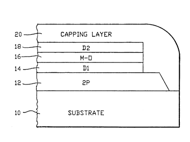
FIG. 1 is a partial sectional view of a preferred
magneto-optic storage medium constructed in accordance
with the teachings of the present invention.
FIG. 2 is a graphical representation of the RBS
spectra of SiO2 - ZrO2 films with different compositions.
FIG. 3 is a graphical representation illustrating
the dependence of the index of refraction (at 633nm) on
deposition rate and composition for ZrO2 - SiO2 thin
films made by reactive sputter deposition from individual
elemental targets.
FIG. 4 is a graphical representation illustrating
the dependence of the index of refraction (at 633nm) on
deposition rate and composition for ZrO2 - SiO2 thin
films made by reactive sputter deposition from Zr-Si
elemental alloy targets.
FIG. 5 is a graphical representation illustrating
the index of refraction as a function of annealing film
containing 20 % SiO2.
FIG. 6 is a graphical representation illustrating
the enhanced corrosion protection afforded by amorphous
mixed SiO2 - ZrO2 film.
FIGS. 7A and 7B are graphical representations
illustrating the enhancement of Kerr rotation provided by
the application of mixed SiO2 - ZrO2 film.
FIG. 8 is a graphical representation illustrating
the dependence of the index of refraction (at 633nm) on
composition for TiO2 - SiO2 thin films made by reactive
sputter deposition from various alloy targets.
Detailed Description
Y09-89-133 - 5 - 203~
Referring now to the figures and to FIG. 1 in
particular, there is shown in partial section a preferred
magneto-optic storage medium construction in the form of
a multi-layer stack comprising a substrate 10, a plastic
first layer 12 (also referred to as a 2P layer) disposed
on the substrate, a first dielectric layer 14 (also
referred to as a Dl layer) disposed on the 2P layer, a
magneto-optic thin film material 16 disposed on the Dl
layer, and a second dielectric layer 18 (also referred to
as a D2 layer) disposed on the magneto-optic material
layer. The layers 12, 14, 16 and 18 are covered by a
protective or capping layer 20.
Magneto-optic storage is accomplished by using a
laser light source to change the magnetic orientation of
selected portions of a magneto-optic thin film material
which has been deposited on a substrate.
Actual information storage is accomplished by using
focused laser radiation as a heat source to raise the
temperature of selected portions (bits) of the
magneto-optic film to a temperature where it no longer
maintains a vertical magnetization and then reorienting
the heated bit of material in the reverse direction
compared to the unheated portion of the film. This will
cause the reoriented piece of material to interact
differently with a lower intensity read laser beam
thereby allowing binary storage states. There are two
types of magneto-optic effects which are utilized in
storage: the Kerr effect, in which polarized light is
reflected off the surface of the magneto-optic film and
the rotation of the reflected beam is measured, and the
Faraday effect, in which the rotation of polarized light
passing through the magneto-optic film is measured. A
slight variation of the second method utilizes a
reflecting layer between layers 18 and 20 shown in FIG. 1
or alternatively the material of layer 20 is selected to
perform the reflection function as well as capping. Such
a layer allows for multiple passes of light through the
magneto-optic film thereby enhancing the Faraday signal.
~09-89-133 - 6 - 2032~6~
In the Faraday mode the magneto-optic layer and D2 layers
are thinner than in the Kerr mode as the light beam must
pass through them. It should be noted that the optimum
indicies of refraction and thicknesses for layers 16 and
18 are not the same in all cases. Therefore, the ability
to adjust the index of refraction of dielectric layers is
desirable and allows for attainment of maximum
performance in terms of signal to noise ratio, optical
efficiency, thermal considerations and the like for a
given storage medium design. The method of constructing
the magneto-optic storage medium and the preferred
materials comprising each of the layers will be described
hereinafter.
The substrate 10 preferably comprises glass or
plastic and is of sufficient thickness, as will be
apparent to one skilled in the art, to provide structural
and mechanical integrity to the completed medium
structure. The plastic layer 12, which is usually
grooved, is typically a photosensitive polymer material
which may be patterned by standard photolithographic and
etching techniques and is typically 1 to 2 ~m thick. The
function of the grooves is to keep the laser head on the
correct track while reading and/or writing on the medium.
Previously, the dielectric layers 14 and 18 have
usually been constructed of electrically insulating
materials such as, but not limited to, silicon oxide,
carbide, nitride, aluminum oxide, titanium dioxide and
zirconium oxide. The index of refraction of the
dielectric layer is critical in terms of optimizing the
amount of light which is coupled to the magneto-optic
layer 16 disposed between the two dielectric layers 14
and 18, and assumes an optimum value depending on the
exact stack configuration, i.e., utilizing the Kerr or
Faraday effects for data storage. The signal-to-noise
ratio of an erasable magneto-optic storage medium is
proportional to ~R where R is the reflectivity of the
medium and ~ is the angle of rotation.
Y09-89-133 - 7 - 232866
The storage medium is preferably constructed
according to the following procedure. Plastic layer 12 is
photo-etched onto substrate 10 to form a plurality of
grooves at preselected locations on the surface of the
substrate. First dielectric layer 14 is sputter deposited
onto the plastic layer 12 directly from compound targets
or reactively from elemental targets and is typically
less than 1000 A thick. A thin film layer of
magneto-optic material 16 is deposited onto the first
dielectric layer 14. A second dielectric layer 18 is then
deposited onto the magneto-optic material 16 in a manner
similar to the deposition of the first dielectric layer.
The first dielectric layer 14 and the second
dielectric layer 18 which generally comprise the same
composition may in certain application comprise different
compositions both in terms of the M containing component
and the relative percentages of SiO2 and the M containing
component.
The above described medium of dielectric layers and
magneto-optic film can be replicated in order to form a
stack of such media.
In order to provide further environmental stability
a protective or capping layer 20 is deposited over the
described stack.
The preferred method of manufacturing the dielectric
layer in thin film form is by sputter deposition of
individual or alloy elemental targets in an oxygen
containing plasma and/or sputter deposition of the
compounds themselves sequentially or simultaneously or in
a combination thereof. Physical evaporation and chemical
vapor deposition techniques can also be used to form the
dielectric layers. The dielectric layers are preferably
30-200 nm thick and have an index of refraction in the
range between 1.4 and 2.4 and preferably an index of
refraction of approximately 2.2 for the Kerr mode of
operation and approximately 1.8 for the Faraday mode. It
rO9-89-133 - 8 -
203~36~
is also desirable that the dielectric layers are in an
amorphous state in order to eliminate grain boundaries
found in polycrystalline materials. The presence of grain
boundaries results in the provision of sites for
diffusion of atmospheric contaminants into the
magneto-optic material layer or out-diffusion of
magneto-optic constituents when the medium is heated or
otherwise environmentally stressed.
The magneto-optic material layer 16 comprising any
of the known magneto-optically active materials such as
the rare earth-transition metal alloys such as TbFe,
TbFeCo, GdCo among others as is known to those skilled in
the art of magneto-optic recording. The thickness of the
magneto-optic film layer is typically in the range
between 2 and 200 nm depending on the recording mode and
stack design.
The capping layer 20 is preferably an inexpensive,
easy to deposit material such as aluminum and is
typically greater than 2000 ~ in thickness. The capping
layer provides a dust-free, hermetically sealed
environment for the magneto-optic storage medium.
The present invention concerns the use of compound
glasses having the chemical formula SiO2 - M02 or SiO2
- M203 or SiO2 - M205 and combinations thereof as the
dielectric layer material. The element M is selected from
Zr, Ti, Al, Nb, Y, Sn, In, Ta and Sb and preferably is
Ti, Zr or Al. The advantage manifest by the use of
compound glass dielectric layers is that the tendency of
the M-containing compound to crystallize is suppressed by
the glass forming SiO2. Moreover, the physical, chemical
and structural properties, and in particular the index of
refraction are controllable by suitable adjustment of the
relative percentages of the compound glass components.
The following examples demonstrate the effect of the
component composition in a SiOz - ZrO2 and a SiO2 -TiO2
`~09-89-133 - 9 -
- ~03;~86~;
binary system on the refractive index and density of the
resultant sputtered thin films.
EXANPIE 1
A mixed SiO2 - ZrO2 film of varying composition was
produced by dual source reactive magnetron sputtering in
the following manner. Two high purity elemental targets
of Zr and Si were mounted in a vacuum chamber in
magnetron sputtering sources arranged in a colinear
fashion to allow a compositional gradient to be
established during each deposition run. The vacuum
chamber was evacuated to at least 1 x 10 5 T. A mixture
of Ar and 2 ~ both 99.99~ pure, was used as the sputter
gas. The appropriate gas rations were established by a
series of total pressure versus oxygen flow rate, for
constant argon flow rate, measurements. These
measurements established the pressure ranges in which the
targets were still metallic and ranges in which the
targets oxidized. It is preferred to deposit the mixed
films while the targets are near the metallic state as
higher deposition rates are achieved. Based on these
measurements films were typically produced at total
pressures between 5 and 7 mT with about 0.1 partial
pressure of oxygen, these values were selected as a
matter of convenience and are not indicative of process
limitations. The sputtering power was varied from about
50 W/cm2 to 10 W/cm2 for each target to compensate for
differences in sputter yields for Zr and Si as well as to
provide compositional control. The full range of
compositions from ZrO2 to SiOz and deposition rates from
10 to 750 ~/m could be obtained by adjusting the target
power levels and source to substrate distance. Fully
oxidized films of mixed composition could easily be made
by this technique. FIG. 2 is a graphical presentation of
two Rutherford Backscattering spectra of films made by
the above described techni~ue which show that the films
are fully oxidized and that the composition of each film
is different. The film represented by the solid line has
a composition of 0.94 ZrO2 - 0.06 SiO2 and the film
~09-89-133 - 10 - 203~866
represented by the dotted line has a composition of 0.83
ZrO2 - 0.17 Si 02 FIG. 3 shows the dependence of the
index of refraction, measured at 830 nm, on deposition
rate and composition for SiO2 - ZrO2 films made by
reactive sputter deposition from individual elemental
targets. The dotted line represents the theoretical
values of index of refraction expected for fully dense
bulk samples determined by calculation and published data
for bulk glass samples on the high SiO2 end reported in
the article by M. Nogami entitled, "Glass Preparation of
the ZrO2 -SiO2 System by the Sol-Gel Process from Metal
Alkoides", Journal of Non-Crystalline Solids 69, ~1985)
415-423. It should be noted that either r.f. or d.c.
sputtering could be used, although if d.c. sputtering is
used for the Si then the target should be doped to have a
sufficiently low resistivity for this process. Film
thicknesses were typically in the 50 to 900 nm range for
convenience of measuring optical and physical properties
but are by no means restricted to that range. It was
also determined that approximately 9 atomic percent SiO2
is required in these mixed oxide films in insure the film
is completely amorphous.
EXAMPLE 2
Using the same vacuum chamber cited in example 1 as
well as an ion beam sputter deposition system mixed
composition films were also produced from elemental alloy
targets. The compositions of the sputtering targets were
(i) 87.4% Zr-12.6% Si, (ii) 73.5% Zr-26.5% Si, and (iii)
30% Zr-70% Si (actual atomic %). A 46% Zr-54% Si target
was used for reactive ion beam sputter deposition. Again,
conditions were determined where the ratio of oxygen to
argon in the sputtering gas was sufficient to produce
fully oxidized films using the single composition
targets. The variation in index of refraction was also
as expected as is shown in FIG. 4.
EXAMPLE 3
Y09-89-133 - 11 - 203~866
A key feature of the present invention is the
thermal stability of the amorphous films formed by mixing
SiO2 with the aforementioned M containing compounds.
This is shown in FIG. 5 which is a graph of the index of
refraction of a 20 SiO2 - 80 ZrO2 thin film as a function
of annealing time. Under similar conditions pure ZrOz
films exhibit crystallization and changes in index of
refraction.
EXAMPLE 4
The advantage the present invention provides in the
area of enhanced environmental protection of the
magneto-optic storage media is demonstrated in the
following manner. Several TbFe films about 1000 ~ thick
were coated with 700 to 900 ~ thick films of a reactively
sputter deposited ZrO 854 Sio 146 z and tested for
corrosion resistance as compared to uncoated TbFe and
TbFe coated with an equivalent thickness of ZrOz. The
results are shown in FIG. 6. It can be seen that in
deionized water, the agent used in this test, uncoated
and unprotected TbFe has the highest corrosion rate and
completely dissolves in about 6 minutes. In contrast,
both the ZrOz and SiOz - ZrOz coated films have a much
lower corrosion rate with the mixed oxide film providing
the lowest rate by a factor of two. This improvement is
attributed to the fact that the addition of SiO2 to the
ZrOz changes the phase of the dielectric layer from
polycrystalline to amorphous thereby eliminating grain
boundary diffusion paths to the magneto-optic layer.
EXAMPLE 5
The optical quality of the amorphous SiOz - ZrO2
films was also verified by coating several fused silica
substrates with quarter wave thicknesses (about 950 ~) of
the ZrO 854 Sio 146 2 composition film and then TbFeCo
magneto-optic films. FIG. 7A graphically illustrates
typical Kerr loops of the media without the mixed oxide
layer and FIG. 7B graphically illustrates typical Kerr
Y09-89-133 - 12 -
203~866
loops of the media with the mixed oxide layer. All loops
were measured in the backwall mode in that the
magneto-optic media was addressed through the substrate
and Dl layer as indicated in the figure insert. The
expected optical enhancement was obtained as seen by the
increase in the recorded Kerr rotation from 21.8 minutes
to 42.9 minutes.
EXAMPLE 6
Similar results to those detailed above were
obtained when a series of elemental alloy targets of Ti
and Si were reactively sputtered. In this example it was
found that about 3 at % SiO2 added to TiO2 was sufficient
to produce a thermally stable mixed oxide amorphous film.
FIG. 8 shows the dependence of index of refraction and
density for the SiO2 - TiO2 thin film system as a
function of composition.
Glass network modifiers such as, but not limited to,
BaO, ZnO, and PbO may be added to the compound glass to
allow further control of optical or other properties as
required in a particular situation. The glass network
modifier is added to either or both dielectric layers 14,
18.
While there have been described and illustrated a
preferred dielectric layer for use in a magneto-optic
storage medium and a magneto-optic storage medium, it
will be apparent to those skilled in the art that
variations and modifications are possible without
deviating from the broad principles of the present
invention which shall be limited solely by the scope of
the claims appended hereto.