Note: Descriptions are shown in the official language in which they were submitted.
Z032955
BURSTED AN~ NON-BURSTED DATA ROUTER
This invention was made with Government support
under a contract awarded by the Government. The
Government has certain rights in this matter.
BACKGRO~ND OF THE I~VENTION
Field of the Invention:
The present invention relates to communication
systems. More specifically, the present invention
relates to data routing systems.
While the present invention is described herein with
reference to illustrative embodiments for particular
applications, it should be understood that the invention
is not limited thereto. Those having ordinary skill in
the art and access to the teachings provided herein will
recognize additional modifications, applications and
embodiments within the scope thereof and additional
fields in which the present invention would be of signif-
icant utility.
Description of the Related Art:
Data routing systems route data from an input
channel to an appropriate output channel. Data may be
input and output bursted or non-bursted. For bursted
data, typically all incoming bursts begin and end at the
same time with a number of bursts making up a frame of
burst data. For non-bursted data, the data is typically
made up of packets of data which do not always begin or
.~ .
:
2 2032955
end on a burst boundary. Some data routing systems, for
example those for certain satellite applications, require
the ability to route and format both bursted and non-
bursted data.
Many conventional data routers which handle bursted
data, particularly those built for secure communications,
require the ability to time deshuffle the order of
incoming data bursts and to time shuffle the order of
outgoing data bursts. In addition, output buffers must
format the output data to obtain the proper burst rate
and burst size. The conventional approach for data
routing systems handling bursted data is to provide one
dedicated input frame buffer for each input channel and
two dedicated output frame buffers for each output
channel, with one output frame buffer for data shuffling
and one output frame buffer for data formatting. Thus,
in conventional designs one additional frame buffer is
required for each added input channel and two additional
frame buffers are required for each added output channel.
This becomes prohibitively expensive when frame sizes or
- the number of input/output channels is large because
such additional memory adds significantly to the weight,
size and power requirements of a system. For satellite
systems, these mission critical parameters must be
limited to minimize the high cost of satellite
manufacture and launch.
Thus, there is a need in the art for a data routing
system for bursted data requiring less memory for input
data deshuffling and output data formatting and shuffling
than current data routing systems. This need is
addressed by copending U.S. Patent Application Serial No.
, filed by B. Clebowicz et. al. on
which requires only one input burst buffer per input
channel and one output frame buffer per output channel.
Hcwever, because some data routing systems require the
3 20329SS
ability to handle both bursted and non-bursted data,
there is an additional need in the art for a data routing
system which requires less memory for bursted input data
deshuffling and output data formatting and shuffling and
has the ability to handle non-bursted data as well. In
addition, there is a further need in the art for a data
router which can handle bursted data in which the input
bursts are not time aligned.
SUMMARY OF THE INVENTION
The need in the art is addressed by the bursted and
non-bursted data router of the present invention. The
invention provides a data router that performs input data
deshuffling and output data formatting and shuffling, and
operates with both bursted and non-bursted input and
output data using only one input buffer per input channel
and one frame buffer per output channel. The router
includes input channels for receiving input data, input
burst buffers for storing the input data, input address
controllers for providing input data storage information,
output frame buffers for storing the input data in a
deshuffled order and providing formatted and shuffled
output data, output channels for transmitting the output
data and a router controller for controlling the
operation of the router. The advantageous design of the
data router allows for input and output of -both bursts
and packets of data which do not have tlme aligned
boundaries.
- :
- ' ' '
4 Z03Z9~S
BRIEF DESCRIPTION OF THE D~AWINGS
Fig. 1 shows a typical input for a data router with
burst based input channels.
Fig. 2 shows a typical input for a data router with
both burst based and non-burst based input channels.
Fig. 3 shows a block diagram of an illustrative
embodiment of a bursted and non-bursted data router
constructed in accordance with the teachings of the
present invention.
Fig. 4 shows a block diagram of the input address
controller of the bursted and non-bursted data router of
the presen~ invention.
Fig. 5 shows a block diagram of the output frame
buffer of the bursted and non-bursted data router of the
present invention.
DESCRIPTION OF THE INVENTION
Illustrative embodiments and exemplary applications
will now be described with reference to the accompanying
drawings to disclose the advantageous teachings of the
present invention. Generally, bus-based and other types
of bursted data routers take advantage of the fixed
period of all input bursts to perform routing. Fig. 1
shows a typical input for a data router with hurst based
~` input channels. As shown in Fig. 1, all incoming bursts
from all channPls have fixed lengths and begin and end at
~ the same time with this time period being known as a
- burst period. Generally, a burst or group of bursts is
assigned to one user, and all of the bursts are routed to
:
'
. ' - .
~'
. ~` ' , ''
Z032~55
a destination which may be a single channel or a group of
channels. This is convenient since at the end of one
burst period all input buffers will contain whole bursts,
and each burst of data may then be routed to the
appropriate destination. The period of time including
the burst period and any associated guard time between
burst periods is typically known as a routing cycle.
Fig. 2 shows a typical input for a data router with
both burst based and non-burst based input channels.
Non-bursted data is typically composed of packets of bits
that may not begin or end on a burst boundary.
Therefore, at the end of a burst period, input buffers of
non-bursted channels may contain parts of more than one
data packet, and each part may need to be routed to a
different destination. In order to route each data
packet to the appropriate destination, a data router must
keep track of the variable boundaries of the non-bursted
data and change the destination of the data during the
routing cycle.
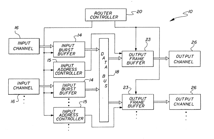
Fig. 3 shows a block diagram of an illustrative
embodiment of a bursted and non-bursted data router 10
constructed in accordance with the teachings of the
present invention. The router 10 incorporates the
advantageous teachings of copending U.S. Patent
Application Serial No. , filed by B. Clebowicz
et. al. on . The teachings of the copending
U.S. Patent Application describe a router which uses less
~ memory to deshuffle bursted input data and format and
- shuffle bursted output data than routers of the prior
art. The teachings of the present invention provide a
bursted and non-bursted data router 10 which also uses
less memory than conventional routers and which handles
both bursted and non-bursted data. The router 10
includes one input buffer 14 and one input address
controller 15 per input channel 16, a data bus 18, a
.~ ' , -~
: ~'
6 203 ~9`~5
router controller 20 and one output frame buffer 23 per
output channel 26. The router 10 operates under the
control of the router controller 20 by first storing each
input burst data or non-burst data received from the
appropriate input channel 16 in the associated input
buffer 14 during a burst period and then transferring
this data through the data bus 18 to the appropriate
output frame buffer 23 at the end of the routing cycle.
The input data is stored in the output frame buffer 23
in a time deshuffled and formatted order. The input
address controller 15 supplies an address offset to the
output frame buffer 23 on subsequent routing cycles to
allow for the storage of non-bursted data that was not
completed in a first routing cycle. Once storage is
complete, the bursted and non-bursted data is read out of
the output frame buffer 23 in a time shuffled and
formatted order for transmission on the appropriate
output channel 26.
During configuration of the router 10, the user
programs the router controller 20 including indicating
the input channel 16 for each burst and packet of data,
; the storage locations in the appropriate output frame
; buffer 23 for this data and the data input and output
rates. The router controller 20 may be implemented by a
sequencer based controller or other type of circuit
without departing from the scope of the present
invention. Thus, during the operation of the router 10,
the controller 20 provides the appropriate timing signals
such that the input bursts and non-burst packets are
received from the input channels 16 by the input buffers
14, stored in the output frame buffers' 23 memory
locations reserved during configuration and transmitted
; on the output channels 26. Those skilled in the art will
appreciate that a customer "black box" may be used to
provide the controller 20 with information for
2032955
controlling the deshuffling and shuffling of data as
required for a specific application.
Fig. 4 shows a block diagram of the input address
controller 15 of the router 10 of the present invention.
The controller 15 includes a packet length data memory
40, an offset counter 42 and a packet counter 44. The
packet length data memory 40 may be implemented by a
random access memory (RAM) or other memory device, and
the offset counter 42 and the packet counter 44 may both
0 be implemented by counters or other circuitry without
departing from the scope of the present invention.
During configuration of the router 10, the packet/burst
lengths are provided by the controller 20 and stored in
the packet length data memory 40 and the number of
packets/bursts is provided by the controller 20 to the
packet counter 44. During operation, the offset counter
42 increments after each bit received by the input buffer
14 by counting transitions on the bit clock input signal
provided by the controller 20. When the offset counter
reaches the current packet/burst length provided by the
packet length data memory 40, a transition is made on the
rollover signal which is sent to the packet counter 44.
The packet counter 44 then increments the current
packet/burst number which is provided to the packet
length data memory 40 such that the current packet/burst
length changes to the new value. When the packet counter
44 rolls over, the counter 44 resets to zero and a new
input frame begins starting with packet zero.
The offset counter 42 provides the offset value as
an output and the packet counter 44 provides the current
packet/burst number as an output. In the case of burst
storage, at the end of a burst period the offset value
will always be zero because a full burst is always stored
in one burst period. ~owever, at the end of a burst
~5 period for non-burst storage, the offset value will not
~ .
Z03Z955
be zero if a full packet was not stored during the burst
period. The offset value will instead indicate where the
storage of the packet data left off. Thus, the offset
value and current packet/burst number can be used by the
5 output frame buffers 23 to provide storage of the input
data in the proper locations in the output frame buffers
23 as described more fully below.
Fig. 5 shows a block diagram of the output frame
buffer 23 of the router 10 of the present invention. The
10 output frame buffer 23 contains a lookup table 30, a
memory buffer 32 and an adder 34. In the preferred
embodiment, the lookup table 30 is a RAM. Those skilled
in the art will recognize that a read only memory (ROM)
or other type of storage device may be utilized for the
15 lookup table 30 without departing from the scope of the
present invention. The memory buffer 32 may be
implemented with a RAM or other type of storage device
without departing f rom the scope of the present
invention. Also, the adder 34 may be a discrete adder
20 circuit or a processor based adder without departing from
the scope of the present invention. Input burst and non-
burst da'a is received by the memory buffer 32 from the
data bus 18 and is stored in a deshuffled order in the
memory buffer 32. The adder 34 provides the storage
25 memory buffer address to the memory buffer 32 as the sum
of the starting memory buffer address from the lookup
table 30 and the offset value provided by the offset
counter 42. For outputting the data, the lookup table 30
provides starting memory buffer addresses c~orresponding
30 to a shuffled order for the output data. The router
- controller 20 controls the loading of the lookup table 30
with the appropriate starting memory buffer addresses and
with providing the proper timing for inputting and
outputting the burst and non-burst data with the proper
35 format.
9 2032955
For the storage of burst or non-burst data in the
memory buffer 32, the channel number provided by the
router controller 20 and the current packet/burst number
provided by the packet counter 44 will be input to the
lookup table 30 which in turn will provide the
appropriate starting memory buffer address for storage of
the input data. The offset value provided by the offset
counter 44 is then added to the starting memory buffer
address by the adder 36 to provide the storage memory
buffer address to the memory buffer 32. For the start of
storage of either burst or non-burst data the offset
value will be zero and storage will begin in the memory
buffer at the starting memory buffer address. However,
for non-burst data where a full packet was not stored
during a burst period, the offset value will provide the
proper offset for resumption of storage of the non-burst
data during the next routing cycle. Where the end of a
packet is reached during a routing cycle, the current
packet/burst number will automatically increment to the
next packet number and the offset counter 44 will reset
- the offset value to zero. Thus, storage will then
continue with data from the next packet stored at the
proper starting memory buffer address. Those skilled in
the art will appreciate that the storage memory buffer
address provided to the memory buffer 32 may be used to
provide the address for the storage of each bit of data
in the memory buffer 32 or it may be used for providing
only the starting address at the beginning of each
routing cycle with the memory buffer 32 or other
circuitry providing subsequent addresses without
departing from the scope of the present invention.
Thus, the present invention has been described
herein with reference to a particular embodiment for a
particular application. Those having ordinary skill in
the art and access to the present teachings will
lo 20~Z955
recognize additional modifications applications and
embodiments within the scope thereof. For example, those
skilled in the art and with access to the teachings of
the present invention may design data routers 10 with the
number of input channels 16 and output channels 26
required for a particular application. In addition, the
design of the router controller 20 may allow for
deshuffling, formatting and shuffling of the input and
output data including providing proper burst sizes and
data rates as appropriate for a particular application
without departing from the scope of the present
invention. Clearly, the bursted and non~bursted data
router 10 of the present invention is not for use solely
in satellite systems, but may be utilized in other types
of communication systems.
It is therefore intended by the appended claims to
cover any and all such applications, modifications and
embodiments within the scope of the present invention.
.