Note: Descriptions are shown in the official language in which they were submitted.
20332~6
OPTICAL SEMICONDUCTOR DEVICE
FIELD OF THE INVENTION
This invention relates to an optical
semiconductor device, and more partlcularly to, an
optical semiconductor device applicable to an optical
modulator, an integrated type optical modulator, an
optical detector, etc.
BACKGROUND OF THE INVENTION
In accordance with the development of optical
communication systems in recent years, optical
modulators which operate at an ultra-high speed and by
a low voltage, and are small in size and easily
integrated with other devices, optical detectors which
operate at a high speed, etc. are highly required to be
put into practical use. In optical semiconductor
modulators, an optical modulator which utilizes an
effect of increasing light absorption loss in an
optical waveguide by applying a voltage to the optical
waveguide (Franz-Keldysh effect or Quantum confined
Stark effect) has advantages in that, if a device
capacitance is decreased, it operates with a several
tens GHz modulation bandwidth, and it can be integrated
with a DFB laser, etc. For instance, a 20 GHz optical
modulator using a InGaAlAs/InAlAs multiple quantum well
structure is described in "a preliminary lecture paper
`i. ~:=,
2 2033~46
C-474 of the spring national conference, 1989 in the
Institute of Electronics Informations and
Communications
Engineers" by Wakita et al. This modulator is an
absorption type modulator utilizaing the shift of an
absorption peak induced by an electric field generated
by a reverse bias voltage applied to a semiconductor
PIN structure, and comprises an n-InAlAs cladding
layer, a multiple quantum well layer and a p-InAlAs
cladding layer successively grown on an n-InP substrate
by MBE method. A modulation frequency band ~ f of this
modulator is almost determined by a device capacitance
C, and is defined by a below equation.
~ f = 1/~CR
The device capacitance C is expressed by a sum
of a junction capacitance Cj of a pn junction in the
stripe-optical waveguide, an interconnection
capacitance Ci of an interconnection connecting a
stripe-electrode to a bonding pad, and a pad
capacitance Cp at the bonding pad.
In this modulator, the device capacitance is as
low as 0.2pF to provide an ultra-high speed modulation,
because it has a structure of a low capacitance having
a polyimide burying layer under the bonding pad. Even
in this structure, however, the junction capacitance Cj
which is inherent to a modulator is less than a half of
the whole device capacitance C, and the remaining is
203324~
the interconnection and pad capacitances Ci and Cp
which are unnecessary for the device and is produced
among the n-InP substrate, the interconnection, and the
electrode. Considering the switching characteristics
of this modulator, a large decrease of the junction
capacitance Cj is difficult, because this modulator has
a device length of approximately 100~m. In addition,
the decrease of the interconnection and pad
capacitances Ci and Cp is also difficult, because a
conductive substrate such as the n-InP substrate is
used.
For this reason, a conventional optical
modulator has a modulation band of 20 to 25 GHz at
most, so that it can not be applied to an ultra-high
speed optical modulator having a modulation band of
more than 50 GHz.
Another conventional optical modulator is
described in "IOOC '89, Technical digest 20PDB-5, 1989"
by Soda et al. This optical modulator is integrated
with a DFB laser on an n-InP substrate, and is a
modulator utilizing light absorption of Franz-Keldysh
effect and having burying layers of semi-insulating InP
on the both sides of an optical waveguide for the
modulator and the DFB laser. Even in this integrated
modulator, a polyimide layer is provided under an
electrode pad to decrease a large parasitic
capacitance, because a large capacitance is generated
4 203324fi
due to the use of the conductive substrate. As a
result, a device capacitance is approximately 0.55pF,
and a modulation band is approximately 10 GHz.
As described above, a limitation occurs in
decreasing a device capacitance, because a conductive
substrate is used. A limitation also occurs in
expanding a modulation frequency bandwidth, as
explained to be approximately 25 GHz in the former
modulator and approximately 10 GHz in the latter
integrated type modulator, because a thickness of the
semi-insulating layer between the electrode provided on
the conductive substrate and the other electrode
provided on the stripe-mesa portion and the semi-
insulating layer is only 2 to 3~m on the both sides of
the stripe-mesa portion, so that it is difficult to
decrease the device capacitance to less than 0.5pF.
Although the device capacitance is more decreased by
increasing the thickness, another limitation occurs in
fabricating the devices due to the increase of a mesa
height.
In order to overcome these disadvantages, an
absorption type optical modulator using a semi-
insulating InP substrate is proposed on pages 270 to
272 of "IEEE PHOTONICS TECHNOLOGY LETTERS, Vol 1, No.9,
September 1989" by Lin et al. This optical modulator
comprises a lower undoped InP cladding layer, an
undoped InGaAsP absorption layer, an upper undoped InP
2033~ 16
cladding layer, a p-InP cladding layer, and a p-InGaAsP
cap layer successively provided on the semi-insulating
InP substrate, and has a ridge type optical waveguide
formed by removing portions of the p-InGaAs cap layer,
the p-InP cladding layer, and the upper undoped InP
cladding layer by etching. The optical modulator
further comprises a p-electrode provided on the p-
InGaAsP cap layer, and an n-electrode provided on the
undoped InGaAsP absorption layer.
In this optical modulator, it is considered that
a resistance of the n-side semiconductor layers is
large, and a serial resistance of this device is large,
although a device capacitance is as low as 10fF, when
an electric field is applied to this device. In this
case, a disadvantage occurs in that high speed
operation is difficult to be realized due to the large
resistance, in spite of the small device capacitance.
Otherwise, if the undoped layers becomes n-
layers in this optical modulator, the serial resistance
and the expansion of a depletion layer are considered
to be deviated in run-to-run operation. Thus, the
reproducibility of a modulation frequency bandwidth and
an operation voltage is lowered to result in the low
practicability.
SUMMARY OF THE INVENTION
Accordingly, it is an object of this invention
6 20332~6
to provide an optical semiconductor device such as an
optical modulator, an integrated type optical
modulator, an optical detector, etc. by reducing an
interconnection capacitance and a bonding pad
capacitance.
It is a further object of this invention to
provide an optical semiconductor device such as an
optical modulator, an integrated type optical
modulator, an optical detector having a wide bandwidth
property and a high practicability.
According to this invention, an optical
semiconductor device, comprises: a stripe-mesa
structure provided on a semi-insulating semiconductor
substrate, the stripe-mesa structure including at least
a first conduction type cladding layer, an undoped
light absorption layer, a second conduction type
cladding layer, and a second conduction type cap layer;
semi-insulating burying layers provided on both sides
of the stripe-mesa structure; and means for applying a
predetermined electric field to the undoped light
absorption layer.
In this invention, a semi-insulating
semiconductor substrate is used, and an optical
waveguide of a PIN structure is buried on its both
sides with semi-insulating layers, such that a
capacitance of portions having no connection with
operation of an optical semiconductor device such as an
203324~
optical modulator, an integrated type optical
modulator, an optical detector, etc. is decreased as
much as possible to decrease a total capacitance of the
device. This provides an optical semiconductor device
having a property of a wide bandwidth.
In general, a capacitance C is expressed by a
below equation.
C = S~O S/d
where ~s is a specific inductivity, ~ O is a
dielectric constant of vacuum, S is an area of each
electrode (or a pn junction area), and d is a distance
between electrodes (or a depletion thickness). As
described in the conventional optical modulator, a
total capacitance Ct of a device is expressed by a
below equation.
Ct = Cj + Ci + Cp
where Cj is a junction capacitance, Ci is an
interconnection capacitance, and Cp is a bonding pad
capacitance. The junction capacitance Cj has an effect
on a static characteristic of an optical modulator.
Therefore, the optical modulator is designed to provide
no deterioration of the static characteristic, such
that an optical waveguide width is 2 ~m, an optical
waveguide length is 100 ~m, and a depletion layer
thickness is 0.3 ~m. Thus, the junction capacitance Cj
of approximately 74 fF is obtained. The
interconnection and pad capacitances Ci and Cp are
203324~
desired to be decreased for a wide bandwidth property
of the optical modulator.
In this invention, the distance a between the
electrodes is as long as approximately 100 ~m, so that
the interconnection and pad capacitances Ci and Cp are
decreased to be one-tenth of those in the conventional
optical modulator using a conductive substrate and a
dielectric burying layer such as polyimide, etc.
provided only under a bonding pad (d is 2 to 3~m and
10 S is equal to or nearly 3), and one-thirtyth of those
in the conventional optical modulator using a semi-
insulating burying layer of a semiconductor provided
only under a bonding pad (d is 2 to 3~ m, and ~3 is
equal to or nearly 12). Consequently, the total
capacitance Ct of the device is determined almost by
the junction capacitance Cj, so that an optical
semiconductor device having a wide bandwidth property
is obtained.
An optical waveguide of a PIN structure provided
on asemi-insulating substrate and buried with semi-
insulating layers is similar in structure to a
semiconductor laser. Therefore, an optical modulator
according to the invention is easily integrated with a
semiconductor laser to provide an integrated type
optical modulator operating at an ultra-high speed.
A structure of an optical modulator according to
the invention can be used as a waveguide type optical
203324fi
,<~ ,
detector, if a light absorption layer is composed of a
material having a bandgap wavelength which is longer
than a wavelength of a light source, and photocurrent
induced by light absorbed in the light absorption layer
is detected by p-and n-electrodes.
BRIEF DESCRIPTION OF THE DRAWINGS
This invention will be explained in more detail
in conjunction with appended drawings, wherein:
Fig. 1 is a schematic view of an optical
modulator in a first preferred embodiment according to
the invention;
Figs. 2A to 2E are schematic cross-sectional
views showing steps of fabricating the optical
modulator in the first preferred embodiment;
Fig. 3 is a schematic view of an optical
modulator in a second preferred embodiment according to
the invention;
Figs. 4A to 4D are schematic cross-sectional
views showing steps of fabricating the optical
modulator in the second preferred embodiment;
Figs. 5A to 5C are schematic cross-sectional
views showing an integrated type optical modulator in a
first preferred embodiment according to the invention;
Fig. 6 is a schematic view showing an optical
modulator in a third preferred embodiment according to
the invention;
,() 20332~16
Figs. 7A to 7C are schematic cross-sectional
views showing steps of fabricating the optical
modulator in the third preferred embodiment;
Figs. 8A and 8B, 9A and 9B, and 10A and 1OB are
schematic cross-sectional views showing steps of
fabricating semi-insulating substrates having buffer
layers of a first conduction type;
Fig. 11 is a schematic view showing an optical
modulator in a fourth preferred embodiment according to
the invention;
Figs 12A to 12C are schematic cross-sectional
views showing steps of fabricating the optical
modulator in the fourth preferred embodiment; and
Fig. 13 is a schematic view showing an optical
detector in a first preferred embodiment according to
the invention.
DESCRIPTION OF THE PREFERRED EMBODIMENTS
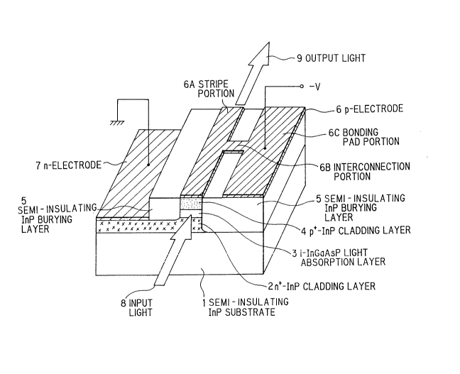
Fig. 1 shows an optical modulator in the first
preferred embodiment according to the invention. The
optical modulator comprises a semi-insulating InP
substrate 1, an n+-InP cladding layer 2, an i-InGaAs
light absorption layer 3, a p+-InP cladding layer 4,
semi-insulating InP burying layers 5, a p-electrode 6,
and an n-electrode 7. The p-electrode 6 has a stripe
porion 6A, an interconnection portion 6B, and a bonding
pad portion 6C.
~ 1 20332~
In this optical modulator, an incident light 8
is modulated to be supplied as an output light 9
dependent on a light absorption coefficient changing
based on an electric field generated by a voltage -V
applied across the p- and n-electrodes 6 and 7.
In the optical modulator of the first preferred
embodiment, though an optical waveguide of a double-
hetero structure using a InGaAsP/InP system material is
explained,the material and the structure may be
replaced by an InGaAs/InAlAs system material, a
GaAs/AlGaAs system material, etc. and by a multiple
quantum well structure, etc.
The fabrication steps of the optical modulator
will be explained in Figs. 2A to 2E.
An n+-InP cladding layer 2 having a thickness of
0.5 ~m, an i-InGaAsP light absorption layer 3 having a
bandgap wavelength of 1.475 ~m and a thickness of 0.3
~m, and a p+-Inp cladding layer 4 having a thickness of
1.2 ~m are successively grown on a semi-insulating InP
substrate 1 by MOVPE method. Then, a stripe-mask 10 of
SiO2 having a stripe-width of 2 ~m is formed on the p+-
Inp cladding layer 4 to provide an optical waveguide by
ordinal photolithography method, and a resist mask 11
is provided on the stripe-mask 10 and on one side of
the p+-InP cladding layer 4 relative to the strip-mask
10, as shown in Fig. 2A.
The p+-InP cladding layer 4 is removed on the
20332~6
other side having no resist mask to provide a thinned
p+-InP cladding layer 4 having a thickness of 0.5~ m by
etching, as shown in Fig. 2B.
The resist mask 11 is removed, and etching is
carried out to provide a three-dimensional optical
waveguide by use of the SiO2 stripe-mask 10. At this
time, a depth of the etching is controlled to be
approximately 1.6~ m, so that the n-InP cladding layer
2 is exposed on one side of the stripe-mask 10, and the
semi-insulating InP substrate 1 is exposed on the other
side of the stripe-mask 10, as shown in Fig. ZC.
The SiO2 stripe-mask 10 is used for a selective
epitaxial mask to bury the stripe-mesa portion with Fe-
doped semi-insulating InP burying layers 5 on the both
sides of the stripe-mesa portion, as shown in Fig. 2D.
The SiO2 stripe-mask 10 is removed, and a p-
electrode 6 is provided on the semi-insulating InP
burying layer 5 which is directly in contact with the
semi-insulating InP substrate 1. Finally, the semi-
insulating InP burying layer 5 which is in contact with
the n+-InPcladding layer 2is etchedto expose the n+-
InP buffer layer 2, and an n-electrode 7 is provided on
the exposed n+-InP cladding layer 2, as shown in Fig.
2E.
In the optical modulator thus fabricated, a
distance between the p-and n-electrodes 6 and 7 is
approximately 100~ m, the substrate 1 is polished to be
'~ 233~2~6
approximately 100 ~m in thickness, and a device length
is made to be100~m by cleaved facets. The p-electrode
6 has an area of 100 ~m x 2 ~m on the stripe-mesa
portion, that of 10 ~m x 20 ~m on the interconnection
portion, and that of 100~m x 100~m on the bonding pad
portion, such that a capacitance is decreased due to
the decrease of a total area based on the separation of
the above three portions.
In operation, a static characteristic of the
optical modulator will be first explained. Here, it is
assumed that a wavelength of the incident light 8 is
1.5~ m used for optical communication. When no reverse
bias voltage is applied across the p- and n-electrodes
6 and 7, the incident light 8 supplied to the optical
modulator is supplied therefrom as the output light 9
without any modulation. In this case, a loss of light
transmitted through the optical modulator is as low as
approximately 1.5 dB in accordance with the parameters
that the device length is 100 ~m, and a wavelength
detuning between the incident light 8 and a bandgap
of the optical waveguide layer is 75 ~m. When an
electric field is applied to the i-InGaAsP light
absorption layer 3 by applying a reverse bias voltage -
V across the p- and n- electrodes 6 and 7, no output
light 9 is obtained, because the light is absorbed in
the i- InGaAsP light absorption layer 3 by Franz-
Keldysh effect. In this case, a satisfactory result
2033~46
that a light extinction ratio is more than 10 dB is
obtained, when the reverse bias voltage is -3V.
Next, a modulation characteristic will be
explained. As described before, the modulation
frequency bandwidth ~f is determined by the below
equation.
Af = 1~ CR
In this preferred embodiment, if it is assumed
that a specific inductivity of a semiconductor is 12.5,
the junction capacity Cj is 74 fF, and the
interconnection and pad capacitances Ci and Cp are
totally 12 fF. Thus, the total device capacitance is
86 fF. As a result, a device capacitance determining a
modulation speed becomes one-fifth to tenth as compared
to that of the conventional optical modulator.
Consequently, the modulation frequency bandwidth Af of
74 GHz is obtained to provide an optical modulation
having an ultra high speed modulation property.
Fig. 3 shows an optical modulator in the second
preferred embodiment according to the invention. The
fabrication steps of this optical modulator will be
explained in Figs. 4A to 4D.
An n+-InP cladding layer 22 having a thickness
of 1.0 ~m, an i-InGaAsP light absorption layer 23
having a bandgap wavelength of 1.475~ m and a thickness
of 0.3 ~m, and a p+-InP cladding layer 24 having a
thickness of 1.2 ~m are successively grown on a semi-
- 15
2033246
insulating InP substrate 21 by MOVPE method, and a
stripe-mask 31 of SiO2 having a width of 2 ~n is formed
on the p+-InP cladding layer 24 to provide an optical
waveguide by ordinal photolithography method. Then, a
three-dimensional optical waveguide is provided by
etching using the SiO2 stripe-mask 31, as shown in Fig.
4A. At this time, a depth of the etching is
approximately 1.81~m, so that the n+-InP cladding layer
22 is exposed.
The stripe-mesa structure is buried on the both
sides with semi-insulating InP burying layers 25 by use
of the SiO2 stripe-mask 31. Then, the SiO2 is removed,
and a stripe-mask 32 of SiO2 having a width of 20 ~m is
provided to cover the stripe-mesa. The semi-insulating
InP burying layers 25 and a small upper skin portion of
the exposed n+-InP cladding layer 22 are etched to
provide a relatively wide stripe-mesa structure by use
of the SiO2 stripe-mask 32, as shown in Fig. 4B.
A mask 33 of SiO2 including the SiO2 mask 32 is
provided on the relatively wide stripe-mesa structure
and on the n+-InP cladding layer 22, such that one side
of the cladding layer 22 is covered with the mask 33,
and the other side thereof is exposed. Then, the other
side of the cladding layer 22 is etched by use of the
SiO2 mask 33, as shown in Fig. 4C.
The SiO2 mask 33 is removed, and a p-electrode
26 is provided on the exposed p+-InP cladding layer 24
16 2033246
of the stripe-mesa structure, and on the semi-
insulating burying layer 25 and the semi-insulating InP
substance 21 of the side having no n+-InP cladding
layer 22 via a passivation film 28 of SiO2. Finally,
an n-electrode 27 is provided on the n+-InP cladding
layer 22 which is on the side opposite to the p-
electrode 26, as shown in Fig. 4D. The p-electrode 26
has a stripe-portion 26A, an interconnection portion
26B, and a bondingpad portion 26c, as shown in Fig. 3.
In the optical modulator thus fabricated, the
semi-insulating InP substrate 21 is polished to be
approximately 100~ m in thickness, and a device length
is made to be 100 ~ m by cleaved facets. The p-
electrode 26 has an area of 100 ~m x 2 ~m on the
stripe-mesa portion, that of 10 ~m x 20 ~m on the
interconnection portion, and that of 100~m x 100~m on
the pad portion.
In operation of the optical modulator in the
second preferred embodiment, the same static
characteristic as in the first preferred embodiment is
obtained, because the composition and the layer
thickness of the i-InGaAsP light absorption layer 23
are the same as those in the first preferred
embodiment. That is, a transmission loss between an
incident light 29 having a wavelength of1.55 ~m and an
output light 30 is as low as approximately 1.5 dB, and
a light extinction ratio is more than 10 dB, when a
17 2 0 3 3 2 ~ ~
reverse bias voltage of -3V is applied across the p-
and n-electrodes 26 and 27.
On the other hand, a modulation frequency
bandwidth Af of 69 GHz which is a little narrower than
the value in the first preferred embodiment is
obtained, because the device capacitance is increased
to be 92 fF to a small extent as compared to the value
in the first preferred embodiment due to the structure
difference of the interconnection and the pad portions
of the p-electrode 26. This difference can be
compensated by changing a polishing thickness of a
substrate and/or an area of an electrode bonding pad
portion. Consequently, an ultra-high speed optical
modulator having a modulation frequency band of more
than 50 GHz is easily obtained even in the second
preferred embodiment.
In the optical modulators of the first and
second preferred embodiments, a device length, an
optical waveguide width, an electrode bonding pad
portion area, etc. may be changed. An n-side cladding
layer may be composed of an InP layer and an InGaAsP
layer, one layer of which is used for an etching-stop
layer, and an InGaAsP cap layer may be provided on a p-
side InP cladding layer. Further, the semi-insulating
InP burying layers provided on the both sides of the
stripe-mesa structure may be replaced to provide the
same advantage for an optical modulator by dielectric
18 20332~6
material layers such as polyimide, etc.
Figs. 5A to 5C show an integrated type optical
modulator in the first preferred embodiment according
to the invention, wherein Fig. 5A is a cross-sectional
view along a direction of light transmission, and Figs.
5B and 5C are cross-sectional vlews along lines B-B and
C-C in Fig. 5A, respectively.
First, the fabrication steps of this integrated
type optical modulator will be briefly explained.
An n+-InGaAsP cladding layer 42 having a bandgap
wavelength of 1.2 l~m and a thickness of 0.5 ~ m, and an
i-InGaAsP active layer having a bandgap wavelength of
1.55 m and a thickness of 0.3 l~m are grown on a semi-
insulating InP substrate 41 having a grating 41 A at a
region of a semiconductor laser by MOVPE method, and
the i-InGaAsP active layer 42 is left only on the
grating to expose the n+-InGaAsP cladding layer 42 on a
region of an optical modulator having no grating by
etching using a SiO2 mask (not shown). Then, an i-
InGaAsP light absorption layer 44 having a bandgap
wavelength of 1.475 1~ m and a thickness of 0.3 ~m is
selectively grown on the exposed n+-InGaAsP cladding
layer 42. As a result, an optical cascaded connection
is obtained between the i-InGaAsP active layer 43 and
the i-InGaAsP light absorption layer 44. Then, the
SiO2 mask is removed, and a p+-InP cladding layer 45
having a thickness of 1.3~m is grown on the cascaded
19 2033~ 6
connection layer. The steps as explained in Figs. 2A
to 2D are applied to the fabrication process after the
above steps in this preferred embodiment. That is, a
stripe-mesa structure is formed by two etching steps,
such that the semi-insulating InP substrate 41 is
exposed on one side of the stripe-mesa structure, and
the n+-InGaAsP cladding layer 42 is exposed on the
other side of the stripe-mesa structure. Then, the
stripe-mesa structure is buried on the both sides with
semi-insulating InP burying layers 46, and a groove 52
having a depth of 1 ~m and a length of 10~ m is
provided to provide an electric separation between the
optical modulator and the semiconductor laser.
Finally, p-and n-electrodes 47 and 48 for the
semiconductor laser, and p- and n-electrodes 49 and 50
for the optical modulator are independently provided,
respectively. The substrate 41 is polished to be
approximately 100~ m in thickness, and a device length
is made to be 400 ~ m including 300 ~ m for the
semiconductor laser and 100 ~m for the optical
modulator. The p-electrode 49 has an area of 100 ~m x
2~m for the stripe-mesa portion, that of 10~m x 20~ m
for the interconnection portion, and that of 100~ m x
100~m for the pad portion.
In operation, when a forward bias is applied to
the laser diode, the stimulated emission occurs, so
that a output light 51 is supplied through the light
20 2033246
absorption layer 44 which is cascade-connected to the
active layer 43. A threshold current of the laser
dlode is 50 mA, a lasing wavelength is 1.55~m, and a
power of the output light 51 is 5mW, when the current
is 100mA. When a reverse bias voltage -V is applied
across the p-and n-electrodes 49 and 50, the light
which is propagated through the light absorption layer
44 is absorbed by the Franz-Keldysh effect to provide
light modulation. Operation of an optical modulator
has been already explained in Fig. 1. Therefore, it is
not explained here. Even in this integrated type
optical modulator, a modulation frequency bandwidth of
more than 50 GHz is obtained to provide an ultra-high
speed modulation. Materials, a structure and a
fabrication method of this integrated type optical
modulator may be changed. For instance, an anti-
reflection film and a high reflection film are provided
on an output facet and a reflection facet,
respectively, to provide a high output device.
The optical modulators as shown in Figs. 1 and 3
may be used as an optical detector. In such an
application, the i-InGaAsP light absorption is designed
to include a composition having a bandgap of, for
instance, 1.67 ~m which is larger than a wavelength of
a light source, so that photocurrent induced by light
which is absorbed in the light absorption layer is
detected by the p- and n-electrodes to realize a
2 1 2 0 3 3 ~ ~ 6
waveguide type optical detector. A structure and a
fabrication process of this optical detector are the
same as those explained in Figs. 1 to 4. In this case,
a device capacitance is decreased to be as low as 90fF.
Consequently, an optical detector having an ultra-wide
bandwidth property is obtained.
Fig. 6 shows an optical modulator in the third
preferred embodiment according to the invention. This
optical modulator is fabricated as shown in Figs. 7A to
7D, and comprises a semi-insulating InP substrate 61,
an n-InGaAsP buffer layer 64 having a composition
corresponding to a bandgap wavelength of a 1.1 u m and a
thickness of 3 ~ m included partially in the upper
portion of the substrate 61, a stripe-mesa structure 69
having a width of 1.5 ~,m and including an n-InP lower
cladding layer 65 having a thickness of 0.5 l~m, an
undoped InGaAsP light absorption layer 66 having an
thickness of 0.3 1~ m and a composition of a 1.4 1~ m
wavelength, a p-InP upper cladding layer 67 having a
thickness of 1.5 l~m and a p+-InGaAs cap layer 68 having
a thickness of 0.5 llm~ Fe-doped semi-insulating InP
burying layers 70 provided on the both sides of the
mesa structure 69 thereby buried, a p-electrode 71
provided on the semi-insulating layer 70 and on the
mesa structure 69, and an n-electrode 72 provided on
the exposed portion of the buffer layer 64. Anti-
reflection films are provided on both facets
22 203324~
corresponding to light input and output planes to
suppress light reflection thereon, and a device length
is 300~m.
This optical modulator is fabricated as shown in
5 Figs. 7A to 7D.
In Fig. 7A, a stripe-groove 62 having a depth of
3 ~m is formed on a semi-insulatong InP substrate 61 by
chemical etching using an etching mask 63 of SiO2, and
the groove 62 is buried to be flat relative to the
substrate 61 with an n-InGaAsP buffer layer 64
selectively by hydride VPE method.
In Fig. 7B, the etching mask 63 is removed, and
an n-InP lower cladding layer 65,an undoped i-InGaAsP
light absorption layer 66, a p-InP upper cladding layer
67, and a p+-InGaAs cap layer 68 are grown on the
substrate 61 buried with the buffer layer 64 by MO-VPE
method.
In Fig. 7C, a stripe-mesa structure 69 is formed
to be positioned over the edge of the stripe-buffer
layer 64 by photolithography and etching, such that a
width of the stripe-mesa structure 69 is 1.5 ~m, and
the high-resistance substrate 61 is exposed on one
side, while the buffer layer 64 is exposed on the other
side. Then, the stripe-mesa structure 69 is buried on
the both sides with Fe-doped semi-insulating InP
burying layers 70.
In Fig. 7D, a portion of the semi-insulating
23 20332~ ~
layer 70 which is positioned on the buffer layer 64 is
removed by use of etchant of,for instance, HcQ for
etching only InP selectively. Then, a p-electrode 71
of Ti/Pt/Au is provided on the cap layer 68 and on the
semi-insulating burying layer 70 by sputtiring method,
and an n-electrode 72 of AuGeNi is provided on the
exposed portion of the buffer layer 64 by thermal VDE
method. Finally, anti-reflection films of SiNx are
provided on both cleaved facets of the device by
sputtering method.
The optical modulator thus fabricated has a
device capacitance of 0.25pF, and a modulation
frequency bandwidth of 26 GHz is obtained, when an
incident light having a wavelength of 1.55~m is
supplied to the device. These performances are
improved as twice as those in the conventional optical
modulator.
In this preferred embodiment, InGaAsP may be
replaced in the buffer layer 64 by n-InP. In the above
described fabrication method, the semi-insulating
substrate 61 and the buffer layer 64 are exposed on the
both sides of the stripe-mesa structure 69 by only one
mesa etching step, and photolithography is easily
carried out at the time of the mesa etching. As a
result, yield and uniformity are improved as twice as
those in the conventional optical modulator.
Figs. 8A and 8B, 9A and 9B, and 1OA and 1OB show
24 2033246
methods for providing a semi-insulating substance
having a flat surface and a stripe-buffer layer of a
first conduction type provided partially in the upper
portion of the substrate.
In Fig. 8A, a groove 73 having a depth of 3~m is
formed on a semi-insulating substrate 61 which is then
covered on its entire surface by a buffer layer 64 of
n-InGaAsP having a thickness of approximately 3~m.
Thereafter, a photoresist 74 (for instance, AZ-series
of Hexist Inc.) is applied on the n-InGaAsP buffer
layer 64 to provide a substantially flat surface by
spin-coating.
In Fig. 8B, the photoresist 74 and the buffer
layer 64 are etched at an uniform velocity by RIBE
(reactive ion beam etching). This uniform velocity
etching is realized by adjusting a mixing ratio of
mixture gas consisting of Ar, 2 and HCl which is used
as reactive gas for the etching. When the semi-
insulating substrate 61 is exposed at a region except
for the groove 73, the etching is finished. If
residual photoresist exists on the buffer layer 64, the
photoresist is removed. The substrate thus obtained is
easy to be controlled in following fabrication steps to
provide better yield and interlayer-uniforminity,
because the flatness degree of the surface is high.
In Fig. 9A, an amorphous Si layer 75 is formed
partially on a semi-inslating substrate 61. The semi-
25 203321 6
insulating substrate 61 having the amorphous Si layer
75 is then covered by a SiN film 76.
In Fig. 9B, a thermal treatment is carried out
at a temperature of approximately 800C to diffuse Si
into the substrate 61. Then, the SiN film 76 and the
amorphous Si layer 75 are removed. The surface of the
substrate thus obtained is completely flat, so that the
formation of a stripe-mesa structure becomes much easy.
Further, the fabrication of a diffraction grating
necessary for the integration with DFB laser, etc.
becomes easy. In the above embodiment, the n-buffer
layer 64 may be replaced by a p-buffer layer. For the
p-buffer layer, impurities such as Zn, Cd, etc. are
diffused into the semi-insulating substrate. In this
case, the conduction types of the other semiconductor
layers are necessary to be reverse.
In Fig. 1 OA, an n-InP buffer layer 64 having a
thickness of approximately 3um is provided on the
entire surface of a semi-insulating substrate 61.
In Fig. 1 OB, ions such as H+, B+, etc. for
increasing a resistance of a semiconductor are injected
at a region having no necessity of the provision of a
buffer layer into the semi-insulating substrate 61 by a
depth of more than a thickness of the buffer layer 64.
AS a result, the n-buffer layer 64 is partially formed
in the upper portion of the substrate 61. A thickness
of the buffer layer 64 can be larger than those
-- 26 2033246
obtained in Figs. 8B and 9B, because ion such as H+ and
B+ is injected deeper than Si+. This provides a large
freedom in designing a buffer layer.
Fig. 11 shows an optical modulator in the fourth
preferred embodiment according to the invention, and
Figs. 12A to 12C show the fabrication method of the
optical modulator.
The optical modulator comprises a semi-
insulating InP substrate 101, a stripe-mesa structure
106 including an n+-InP cladding layer 102, an i-
InGaAsP light absorption layer 103, a p-InP cladding
layer 104, and a p+-InGaAs cap layer 105, semi-
insulating InP burying layers 107 provided on the both
sides of the stripe-mesa structure 106, a p-electrode
108, an n-electrode 109, a dielectric layer 110, and a
beneath layer electrode 112. The p-electrode 108 has a
stripe-portn 121, an interconnection portion 114 of an
air-bridge structure, and a bonding pad 115A, and the
n-electrode 109 has a bonding pad 115B.
In fabricating this optical modulator, an n+-InP
cladding layer 102 having a thickness of 2.0~m and a
carrier concentration of 5 x 1o17cm~3, an undoped
InGaAsP light absorption layer 103 having a thickness
of 0.3~m and a bandgap wavelength of 1.475~m, a p+-InP
cladding layer 104 having a thickness of 2.0~m and a
carrier concentration of 5 x 1017cm 3, and a p+-InGaAs
cap layer 105 having a thickness of 0.3~m and a carrier
27 2033246
concentration of 1 x 1019cm 3 are grown successively on
a Fe-doped semi-insulating InP substrate 101 by organic
metal vapour phase epitaxy (MOVPE) method. Next, a
stripe-SiO2 mask having a width of 2~m is provided on
the cap layer 105 by ordinal photolithography method,
and a stripe-mesa structure 106 is formed to expose the
cladding layer 102 by etching using the stripe-SiO2
mask. Then, this stripe-SiO2 mask is used for
selectively burying the stripe-mesa structure on the
both sides with Fe-doped semi-insulating InP burying
layers 107. Thereafter, a stripe-mesa structure having
a width of 10~m including the stripe-mesa structure 106
and the burying layers 107 is formed to expose the
cladding layer 102 on one side and the high-resistance
InP substrate 101 on the other side by selective
etching using ordinal photolithography method. Next, a
p-electrode 108 of AuZn is provided on the cap layer
105, and an n-electrode 109 of AuGeNi is provided on
the cladding layer 102, respectively, as shown in 12A.
A lower resist 111 having a thickness of 2~m is
patterned to provide air-gap for the air-bridge
interconnection stuructre, and a beneath layer
electrode 112 of Ti/Au having respective thicknesses
O
500A/500A, on which an Au-plating electrode is
provided, is provided by vapor deposition in vacuum.
Then, an upper resist 113 which is patterned on the
beneath layer electrode 112 is used for a mask, so that
28 2o33246
a selective Au-plating layer 120 is provided, as shown
in Fig. 12B.
The upper resist 113 is removed by 2 plasma,
and a predetermined portion of the beneath layer
electrode 112 is removed. Thus, the lower resist 111
is removed to provide an interconnection part 114 for
the air-bridge structure and a bonding pad 115, as
shown in 12C. Then, the semi-insulating InP substrate
101 is polished to be approximately 1001~m in thickness,
and a length of the devide is made to be 1OOllm by
cleaved facets. The p-electrode has an area of 1 on~l m x
2~m at the stripe-portion 121, and that of 50~1m x 501,m
at the pad portion 115, and the interconnection portion
114 has a width of 10~m, a length of 501~m, and a height
of 2~m at the air-bridge structure.
In operation of this optical modulator, a static
characteristic will be first discussed. Here, it is
assumed that a wavelength of an incident light is
1.55~m used for optical communication. When no reverse
bias voltage is applied across the p- and n-electrodes
108 and 109, the incident light is transmitted through
the device as an output light without any modulation.
In this case, a transmission loss is as low as
approximately 1.5dB, because a wavelength detuning
between the incident light and the bandgap of the light
absorption layer is 75~m.
When a reverse bias voltage is applied across
2033246
the p-and n-electrodes 108 and 109 to apply an
electric field to the i-InGaAsP light absorption layer
103, an incident light is absorbed in the i-InGaAsP
light absorption layer 103 during the transmission
through the device by Franz-Keldysh effect, so that no
output light is supplied therefrom. In this case, a
light extinction ratio is more than 10 dB which is a
satisfactory property by a voltage of -3V.
Next, a modulation characteristic will be
explained. As described before, a frequency bandwidth
Af of an optical modulator using a field effect is
determined by a device capacitance C, as defined below.
~f = 1/( ~ CR)
In this preferred embodiment, if a calculation
is carried out in the assumption that a specific
dielectric coefficient of the semiconductor is 12.5, a
jenction capacitance Cj is 74fF, and an interconnection
capacitance Ci and a pad capacitance Cp are tolally
3fF. Thus, a total capacitance of this device
determining a modulation speed is 77fF which is one
fifth to nineth as compared to the conventional optical
modulator, and a modulation frequency bandwidth of 83
GHz is obtained to provide an optical modulator having
an ultra-high speed modulation property.
Fig. 13 shows an optical detector in a preferred
embodiment according to the invention. Parts of this
optical detector is indicated by like referrence
30 20332~6
numerals as used in Fig. 11. The only difference
therebetween is that the light absoprtion layer 116 is
composed of InGaAs having a lattice matching property
relative to InP. The same fabrication method as shown
in Figs. 12A to 12C is adopted to fabricate this
optical detector.
In this optical detector, when a wavelength of
an incident light is 1.55~m, the incident light is
effectively absorbed in the light absorption layer 116
of InGaAs, because a bandgap wavelength of the light
absorption layer 116 is 1.67~m which is on a wavelength
side longer than that of the incident light.
Photocurrent induced by absorbed light is detected by
the p-and n-electrodes 108 and 109. Thus, this device
functions as a waveguide type optical detector. In
this case, if a device length and a thickness of the
InGaAs light absorption layer 116 are the same as those
in the aforementiond first preferred embodiment, a
device capacitance can be less than 0.1 pF to provide
an optical detector having an ultra-wide bandwidth
property.
In the preferred embodiments, n-and p-layers may
be replaced by opposite conduction type layers,
respectively. The light absorption layer may be
replaced by a multi-quantum well structure. Materials
are not limited to InGaAsP/InP, but materials such as
InGaAs/InAlAs, AlGaAs/GaAs, AlGaInP/GaInP/GaAs, etc.
31 2~33246
which are used in ordinal semiconductor lasers and
semiconductor hererojunction detectors may be used.
The Fe-doped semi-insulating InP layer may be replaced
by a semi-insulating semiconductor layer doped with
5 dopant such as Co, Ti, etc., or by a semi-insulating
dielectric material such as polyimide. Although it is
considered that stress is applied to a semiconductor
layer, because a thermal expansion coefficient of
polyimide is different from that of a semiconductor, a
predetermined reliability is obtained in accordance
with the decrease of stress by decreasing a volume of
polyimide as a result of narrowing a width of a groove.
Polyimide is effectively used in an optical modulator
and an optical detector, although a semiconductor is
preferably used in a semiconductor laser which
generally produces heat.
Although the invention has been described with
respect to specific embodiment for complete and clear
disclosure, the appended claims are not to be thus
limited but are to be construed as embodying all
modification and alternative constructions that may
occur to one skilled in the art which fairly fall
within the basic theaching herein set forth.