Note: Descriptions are shown in the official language in which they were submitted.
2a3333~
PCT/US90/02~9
WO ~/139~
F.T.F~CTRONIc ~':;TIT.T. C~MF~A UTIT I7ING ~MI~GF~
COMPR~SSION AND DIGITAL STORAG~
Technical Field
The present invention pertains in general
to the field of electronic still imaging and, more
particularly, to an electronic camera incorporating
digital processing of image signals derived from an
electronic image sensor and digital storage of the
processed signals in a removable storage medium.
Backaro~nd Art
An electronic still camera employing
non-volatile storage of digital image signals is
described in U.S. Patent No. 4,489,351. Analog
color information from three charge-coupled device
(CCD) image sensors is converted into a digital bit
stream and transmitted through a peripheral memory
control unit to an integrated circuit memory. The
memory is one unit of many, e.g., twenty-four memory
units, recessed into a ~cassette" that is separably
attached through an electrical connector to the
camera body. In order to obtain a digital image of
high quality, many pi~els, and thus many bits of
digital information, need to be processed in a short
time. In an article entitled ~Possibilities of the
Digital Electronic Still Camera", by Sumihisa
Hashiguchi (~hashin Kogaku, pp. 110-111, February
1988), the author proposes a multi-layer image
processing integrated circuit including sensors,
analog-to-digital (A/D) converters, and 8-bit buffer
storage cells in respective layers. Since the
output signal from an individual pixel is
transferred "vertically" through an A/D converter to
an included storage cell, real-time throughput is
obtained without high speed operation. The stored
WO ~/139~ PCT/US90/025~r
2~3339
signals can be read out slowly for digital
recording, perhaps after compression, on a storage
drive incorporating a small floppy disk. (Another
e~ample of a digital-based electronic still camera
is shown in published UX Patent Application 2089169,
in which the camera loads the digital image signals
into a bubble memory cassette.)
A static random access memory (SRAM) card,
in the size, and form, of a credit card, is an
attractive storage alternative to the devices
described in the above-related disclosures. For
instance, published European Patent Application
289,944 shows a detachable SRAM module for use in a
digital electronic still camera. The module is
disclosed as a 32 M-bit (4 M-byte) SRAM integrated
circuit card, although such storage capacities in a
card are not commonly available at this time. A 512
K-byte SRAM card is presently available (Mitsubishi
Electronics America, Inc. is one supplier).
However, as pointed out in an article by Sumihisa
Hashiguchi (~Picture Recording and Electric Power
Consumption," Shashin Kogyo, pp. 94-95, April
1988), there is a significant problem with memory
volume. In the case; for e~ample, of recording 780
x 490 picture elements from a CCD image sensor, with
8 bits allocated to each picture element, 382,200
bytes are required for a single monochrome video
frame. This amounts to only one picture on a memory
card (of 512 K-bytes). This is a considerable
obstacle since still photographers are used to
taking many pictures, e.g., 24 or 36 pictures, with
one cassette of conventional film. Moreover, color
pictures would ordinarily require three times the
storage capacity of monochrome pictures.
Dynamic random access memory (DRAM) offers
20333`39
PCr/USgO/02569
WO 90/13964
.
more storage in a reasonable volume, but power
consumption quickly becomes formidable as storage
capacity increases. The Hashiguchi article,
consequently, calls for the development of new
5 techniques of storage based on the compression of
picture information by a factor of 10 or 100. As
Hashiguchi points out, several picture compression
techniques are available at present. For esample,
the aforementioned European Patent Application
10 289,944 suggests an embodiment in which a signal
processor is adapted to accomplish data compression,
such as the Hadamard transform, cosine transform or
orthogonal transform, and coding on the video
signal, which in turn is transferred to and stored
1~ in the detachable SRAM card. (It is also of
interest that U.S. Patent 4,131,919, which issued on
December 26, 1978, proposes the use of source and/or
channel encoding schemes to more efficiently record
digital still image signals on magnetic tape.)
20 Adaptive differential pulse code modulation is
another known compression algorithm for encoding
still images.
The fundamental structure for in-camera
digital processing is ordinarily based on a
25 conventional analog camera, with digital processing
techniques being applied to the functional analog
blocks, such as color separation, white balance,
gamma correction, and so on. This conventional
transposition extends to real-time processing in
30 that in-camera digital processing seeks, insofar as
possible, to emulate real-time analog processing
rates by rapidly accessing the imager, processing
the resultant image signals, and writing the
processed image signals to memory within normal
35 video frame rates. (...albeit, that in the
WO-~/139~ PCT/US90/02
aforementioned Shashin Rogaku article of Feb. 1988,
in U.S. Patent No. 4,489,351, and in UK Patent
Application 2089169, a buffer or temporary memory is
provided to allow transmission of the image data to
the recording device at a desired rate, which due to
device or other limitations is often less than the
image capture rate.) Nonetheless, as recognized by
the Hashiguchi article, the available techniques
neither adequately meet the requirement for
real-time processing as needed by an electronic
still camera nor the requirement for simply
including the compression hardware with the camera.
Disclosure of Invention
The problem with the available techniques
is their focus on real-time throughput. The present
invention departs from this focus by distinguishing
the input function of the camera from the processing
function so that, on the one hand, image signals
from a plurality of still images accumulate at a
rate commensurate with normal operation of the
camera while, on the other hand, the accumulated
image signals are digitally processed at a
throughput rate different than the accumulating
rate. The prior techniques tend, by nature of their
focus upon speed, not only to direct compression
choices to those capable of handling a data stream
at an e~tremely fast rate, such as differential
pulse code modulation (DPCM), but also tend to focus
processing upon one image at a time. By providing a
multi-image input buffer and separating digital
processing from input requirements, the digital
processor not only has more time to operate on
blocks of image signals, in particular transform
encoding the blocks of signals, but also obtains
such processing advantages without disturbing the
20~3339
WO ~/13~ PCT/US90/02569
"stacking up" of images in the input buffer. The
invention further utilizes a removable digital
storage means, such as a SRAM memory card, to store
the compressed image signals. With lO:l
compression, for esample, the byte requirement for a
picture can be reduced by a factor of ten and many
more images can be stored in the memory card.
Brief Description of the Drawings
The invention will be described in relation
to the drawings, in which:
Figure lA is a block diagram of an
electronic still camera employing digital processing
according to the invention;
Figure lB is a block diagram of an
exemplary form of image compression used in
connection with the invention;
Figure 2A is a functional sequence diagram
showing multi-image input buffering;
Figure 2B is a further functional sequence
diagram showing full utilization of the input buffer
and concomitant delay;
Figure 3 is a block diagram showing details
of a specific processing architecture for the
electronic still camera;
Figure 4A is a block diagram of an
electronic still player for use in reproducing
pictures taken with the camera of Figure lA; and
Figure 4B is a block diagram of an
exemplary form of image expansion used in connection
- 30 with the player of Fig. 4A.
Best Mode For CarrYin~ Out the Invention
Because electronic still cameras employing
charge-coupled device (CCD) sensors are well known,
the present description will be directed in
particular to elements forming part of, or
20~3339
PCT/US~/0256
WO ~/13~
cooperating more directly with, apparatus in
accordance with the present invention. Elements not
specifically shown or described herein may be
selected from those known in the art.
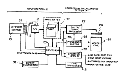
Referring initially to Figures lA and lB,
an electronic still camera is divided generally into
an input section 2 and a compression and recording
section 4. The input section 2 includes an e~posure
section 10 for directing image light from a subject
(not shown) toward an image sensor 12. Although not
shown, the e~posure section 10 includes conventional
optics for directing the image light thr~ugh a
diaphragm, which regulates the optical aperture, and
a shutter, which regulates e~posure time. The
sensor 12, which includes a two-dimensional array of
photosites corresponding to picture elements of the
image, is a conventional charge-coupled device (CCD)
using either well-known interline transfer or frame
transfer techniques. The sensor 12 is e~posed to
image light so that analog image charge information
is generated in respective photosites. The charge
information is applied to an output diode 14, which
converts the charge information to analog image
signals corresponding to respective picture
elements. The analog image signals are applied to
an A/D converter 16, which generates a digital image
signal from the analog input signal for each picture
element.
The digital signals are applied to an image
buffer 18, which is a random access memory (RAM)
with storage capacity for a plurality of still
images. The arrangement for allocating memory space
in the image buffer 18 to individual frames may
vary; for this description, however, the frames will
be allocated to specific, identifiable memory spaces
2Q~3333
WO 90/13964 PCI/US90/02569
-
such that a new frame can be directly written over
an old frame without affecting the other frames in
the buffer 18. This, as will be shown, becomes
convenient in unloading the buffer 18 and freeing
memory space for a new frame as soon as the older
ones are processed.
A control processor 20 generally controls
the input section 2 of the camera by initiating and
controlling e~posure (by operation of the diaphragm
and shutter (not shown) in the exposure section 10),
by generating the horizontal and vertical clocks
needed for driving the sensor 12 and for clocking
image information therefrom, and by enabling the A/D
converter 16 in conjunction with the image buffer 18
for each signal segment relating to a picture
element. (The control processor 20 would ordinarily
include a microprocessor coupled with a system
timing circuit.) Once a certain number of digital
image signals have been accumulated in the image
buffer 18, the stored signals are applied to a
digital signal processor 22, which controls the
throughput processing rate for the compression and
recording section 4 of the camera. The processor 22
applies a compression algorithm to the digital image
signals, and sends the compressed signals to a
removable memory card 24 via a connector 26. A
representative memory card is a 512 K-byte static
random access memory (SRAM) available from
Mitsubishi Corp.
Since the compression and related
processing ordinarily occurs over several steps, the
intermediate products of the processing algorithm
are stored in a processing buffer 28. (The
processing buffer 28 may also be configured as part
35 of the memory space of the image buffer 18.) The
2~)~3339
WO ~/13~ PCT/US90/0256
number of image signals needed in the image buffer
18 before digital processing can begin depends on
the type of processing, that is, for a block
transformation to begin, a block of signals
including at least a portion of the image signals
comprising a video frame must be available.
Consequently, in most circumstances, the compression
may commence as soon as the requisite block, e.g.,
of 16 x 16 picture elements, is present in the
buffer 18.
The input section 2 operates at a rate
commensurate with normal operation of the camera
while compression, which consumes more time, can be
relatively divorced from the input rate. The
exposure section 10 e~poses the sensor 12 to image
light for a time period dependent upon e~posure
requirements, for example, a time period between
1/1000 second and several seconds. The image charge
is then swept from the photosites in the sensor 12,
converted to a digital format, and written into the
image buffer 18 during a standard rate, which may,
for example, correspond to a standard video field or
frame rate. The repetition rate of the driving
signals provided by the control processor 20 to the
sensor 12, the A/D converter 16 and the buffer 18
are accordingly generated to achieve such a
transfer. The processing throughput rate of the
compression and recording section 4 is determined by
the character of an image, i.e., the amount of
detail versus redundant information, and the speed
of the digital signal processor 22, and may take up
to several seconds for an especially comple~ image.
One desirable consequence of this
architecture is that the processing algorithm
employed in the compression and recording section
2~`33 3g ~
WO ~/139~ PCT/US90/02~9
may be selected for quality treatment of the image
rather than for throughput speed. This, of course,
can put a delay between consecutive pictures which
may affect the user, depending on the time between
photographic events. This is a problem since it is
well known and understood in the field of still
video recording that a digital still camera should
provide a continuous shooting capability for a
successive sequence of images. For this reason, the
image buffer 18 shown in Figure l provides for
storage of a plurality of images, in effect allowing
a series of images to "stack up" at video rates.
The size of the buffer is established to hold enough
consecutive images to cover most picture-taking
situations. Figures 2A and 2B show the typical
functional sequence for a camera having buffer area
for three separate images. As each image is
captured (line D), the ne~t available buffer area is
loaded tline E) and image compression begins (line
F). Figure 2A illustrates a typical situation in
which the shutter release (line C) is actuated at
spaced times insufficient to load all three buffer
areas. In Figure 2B, the shutter release is
continuously held down (line C) and a burst of
exposures ensue. The three buffer areas are quickly
loaded (line E) and, responsive to a buffer full
signal (line H), the control processor 20 interrupts
the exposure section lO. No further image is then
captured until a buffer is freed. For example, in
lines E and F, after the first image is compressed
and transferred to the card 24, the first buffer
area is freed up and a fourth exposure is made.
An operation display panel 30 is connected
to the control processor 20 for displaying
information useful in operation of the camera. Such
'2~33339
WO ~/139~ PCT/US~/0256~
--10--
information might include typical photographic data,
such as shutter speed, aperture, e~posure bias,
color balance (auto, tungsten, fluorescent,
daylight), field/frame, low battery, low light,
exposure modes (aperture preferred, shutter
preferred), and so on. Moreover, other information
unique to this type of camera is displayed. For
instance, the memory card 24 would ordinarily
include a directory signifying the beginning and
ending of each stored image. This would show on the
display 30 as either (or both) the number of images
stored or the number of image spaces remaining, or
estimated to be remaining.
The control processor 20 also accesses a
card diagnostics memory 31 for generating important
information about the condition of the memory card
24. Specifically, the connector 26 is queried for
the presence of a card 24 and, if no card is
connected, a "no card" display is produced on the
operation display 30. Likewise, if a card is
present but it is full of images, a "card full"
display is produced. The card diagnostics memory 31
also provides a verification routine to check the
card 24 for faults or defects. For instance, a set
of code patterns (such as OlOlOl...and 101010...)
can be written into and read from the card to verify
memory locations. This is especially important
since compressed data is stored on the card 24 and
even one defective memory location can produce an
extensive visual artifact in the expanded picture.
If a card 24 fails the verification test, a
defective card display is produced on the
operation display 30.
Buffer diagnostics are maintained in a
memory 32 for producing certain information about
- 2 0 3! 3 3 3 9
WO ~/13~ PCT/US90/0250
--11--
the condition of the image buffer 18. Its principal
- purpose is to monitor the utilization of buffer
space and produce, as shown in line H of Figure 2B,
a ~buffer full" signal when no more buffer space is
available. A corresponding display is produced on
the display 30, which is important to the user as no
further image can be captured until a buffer area is
freed up. The digital signal processor 22 further
provides a signal indicative of the compression
operation on a line 30a to the operation display 30,
that is, a signal indicating that compression is
underway. A corresponding display, "compression
underway , is activated by the display 30.
The digital signal processor 22 compresses
each still video image stored in the image buffer 18
according to a known image compression algorithm
shown in Figure lB. The compression algorithm
begins with a discrete cosine transformation (block
33) of each successive block of the image data to
generate a corresponding block of cosine transform
coefficients. It is well-known that compression
techniques are greatly enhanced when applied to
image data which has been previously transformed in
accordance with a discrete cosine transform
algorithm. The cosine transform coefficients are
then rearranged in serial order by a block-to-serial
conversion step (block 34) described and illustrated
in U.S. Patent 4,772,956, "Dual Block Still Video
Compander Processor," issued Sept. 20, 1988 to Roche
et al, and which is assigned to the assignee of the
present invention and incorporated by reference into
the present patent application. The block-to-serial
conversion step consists of arranging the discrete
cosine transform coefficients in order of increasing
spatial frequency, which corresponds to a zig-zag
203~39
WO ~/13~ PCT/US~/0256
-12-
pattern illustrated in the Roche et al patent. The
resulting serial string of transform coefficients is
then subjected to thresholding, normalization, and
quantization (block 36) and minimum redundancy
S encoding (block 38).
Thresholding discards data words of
magnitudes less than a threshold number.
Normalization entails dividing each data word by a
divisor to yield a quotient. Quantization discards
the fractional bits in the quotient. Minimum
redundancy encoding is a technique well-known in the
prior art and employs two complimentary steps,
namely amplitude encoding and run length encoding.
Amplitude encoding (or ~Huffman Encodingn) assigns
to each of a finite set of possible amplitudes an
encoded bit pattern designed to require the smallest
number of bits for non-redundant representation.
Run length encoding represents any consecutive run
of zeros in the data as the smallest non-redundant
bit pattern required to count the number of zeros in
the run. The set of bit patterns representing each
of the possible word amplitudes and the set of bit
patterns representing each of the possible zero run
lengths may be selected in accordance with the
well-known principles and stored in look-up tables
for use during the compression process. This
compression technique greatly reduces the number of
bits required to represent a frame of still video
information, without reduction in image quality,
thereby greatly reducing the amount of storage that
must be allocated to each still frame in the SRAM
card 24.
The uncompressed still video data stored in
the image buffer 18 is organized in the manner of a
television picture, that is, in vertical columns and
2~3~339
PCr/USgO/0256g
WO ~/13~
-13-
horizontal rows of video data bytes (representing
the corresponding picture elements) divisible into
square blocks of bytes, each block comprising, e.g.,
16 columns and 16 rows of bytes. The control
processor 20 fetches a block of data each time the
digital signal processor 22 is about to execute the
compression algorithm. The compression process
eliminates many bits contained in each block of
video data, so that the compressed video data does
not emerge from the processor 22 as a standard-
length stream of bits, but as a variable number of
bits dependent upon the complexity of the picture
and the rules used for truncating bits. The memory
space, therefore, allocated for each image in the
SRAM card 24 can vary from image to image. The
processor 22, consequently, allocates memory space
in the SRAM card 24 after each compression sequence
for an image is completed so that the images may be
"packed" into the card as a continuum of compressed
image data. This means the storage capacity, in
terms of actual images, of the SRAM card is unknown
in the beginning, and then gradually is specified as
pictures are taken and the card is "filled". The
control processor 20 monitors the numbers of images,
furnishing a running total to the operation display
panel 30, and further triggers a special one more
picture" display when the remaining memory space is
sufficient for a predetermined number of, say one
more, pictures. Alternatively, a fixed "maximum"
space can be allocated in the SRAM card 24 for each
image; in this case, fewer images can be stored
although the total capacity is always known.
What has been described to this point
applies equally to monochrome or color pictures,
except that color pictures require additional
WO ~/139~ PCT/US90/02~4
-14-
processing. For instance, if a multi-spectral color
filter array (shown in broken line 39 in Figure lA)
overlies the image sensor 12, the various colors are
sorted out and processed differently for each
color. This would be accomplished by an additional
routine in the digital signal processor 22. Such
color filter array processing would precede the
discrete cosine transform block 33 (Fig. lB) so that
image compression can be done separately on each
color and three compressed frames would be stored in
the memory card 24 for each image.
~ igure 3 illustrates details of a specific
processing architecture in which an image buffer 39
combines the function of the image buffer 18 and the
processing buffer 28 shown in Figure lA. The analog
signals from the output diode 14 of the image sensor
12 are gamma-corrected in a conventional
linear-to-gamma correction circuit 74 and applied to
the A/D converter 16. The output of the A~D
converter 16 is connected to an 8 bit-to-32 bit
latching array 76 comprising latches 76a, 76b, 76c,
and 76d. In practice, the latching array 76
performs a double buffering operation to save time,
that is, the latched bytes are unloaded in pairs to
the processor 22 on a 32 bit-wide input data bus
22a, as follows. After latches 76a and 76b are
loaded with the first two bytes provided by the A/D
converter 16, the latched bytes are applied in
parallel to the data bus 22a. In the meantime, the
other two latches 76c and 76d are being loaded with
the next two bytes. When the latches 76c and 76d
are full, the latched bytes are applied in parallel
to the input data bus 22a while the other latches
76a and 76b are being loaded with new bytes.
In this architecture, therefore, the
2033339
PCT/US90/02569
WO ~/13~
digital signal processor 22 has the initial
function, prior to compression, of transferring the
paired input bytes to the image buffer 39, which
includes random access memories (RAMs) 78a, 78b,
78c, and 78d. In terms of allocating bytes to
storage, RAM 78a receives data from the latch 76a,
RAM 78b from latch 76b, and so on. The digital
signal processor 22 produces address words on an
address bus 22c connected to the RAMs 78a-78d. The
address word is held in an address latch 80 while a
portion of the address word is decoded in a decoder
82 for activating the appropriate chip enable ports
of the image buffer RAMs 78a-78d. As shown in
Figure 3, the buffer 39 is enabled in pairs of RAMs
lS 78a-78d to correspond to the paired bytes being
transferred from the latches 76a-76d.
The embodiment of Figure 3 includes no
resident non-volatile memory for the digital
processor 22. Consequently, the operating program
code for the camera is stored in a programmable read
only memory (PROM) 84 connected to the address and
data buses of the control processor 20. These bus
lines are also connected, through respective buffers
86 and 88, to the output address bus 22c and the
output data bus 22d of the digital processor 22.
The control processor 20 downloads portions of the
operating program from the PROM 84 to the image
buffer 39 as required for operation of the digital
processor 22. For instance, when a shutter release
73 is depressed and a line 73a is activated, the
control processor 20 downloads the data acquisition
code over the data bus 22d to a specified location
in the image buffer 39. The appropriate address
words are then applied to the address bus 22c by the
control processor 20 and the operating code is
2~33339
WO ~/139~ PCT/US90/02
written into volatile memory in the digital
processor 22. The processor 22 is then ready to
latch incoming image bytes into the latch array 76
and transfer paired bytes to the image buffer 39.
When all the image bytes of a still picture
are in the image buffer 39, the control processor 20
downloads the operating code for the discrete cosine
transform from the PROM 84 to a specified unused
memory space in the image buffer 39. The DCT code
is written into the volatile memory of the processor
22 and the discrete cosine transformation is
performed on blocks of image bytes in the image
buffer 39. After each block is transformed, the
transform coefficients are written back into the
image buffer 39. The control processor 20 ne~t
downloads the operating code for the block to serial
conversion in like manner, the conversion is
performed, and the serial string is written back
into the buffer. Then the code for thresholding,
normalization and quantization is downloaded in
similar fashion, the processing done and processed
data stored, and the code for minimum redundancy
encoding is downloaded and the amplitude and run
length encoding is done. With the image data now in
its finally compressed form, and instead of writing
the compressed data back into the buffer 39 one more
time, the compressed data is directly written into
the memory card 24. The above-related technique for
storing the operating code in the PROM 84 and
downloading sections thereof as needed conserves on
the need for fast, and therefore expensive,
non-volatile memory dedicated to the processor 22.
A simplified block diagram is shown in Fig.
4a of a still video player for reproducing a picture
or for making a hard copy print from the digital
2033339
PCT/US90/0250
WO 90/13g64
.
image signals stored in compressed format in the
memory card 24. With the card 24 inserted into a
connector 100, the digital signals are accessed and
processed in an e~pander 102. An e~pansion
algorithm, which is basically the inverse of the
compression algorithm of Fig. lB, is shown in Fig.
4B and implemented by the e~pander 102. The digital
image data is e~panded block-by-block and stored in
an image buffer 104 as a decompressed image. A
conventional thermal printer 106 is connected to the
buffer 104 for making a hard copy thermal print from
the decompressed image. In addition, the
decompressed image signals are converted to analog
form by a digital-to-analog (D/A) converter 108 and
displayed on a conventional CRT monitor 110.
The invention has been described in detail
with particular reference to a presently preferred
embodiment, but it will be understood that
variations and modifications can be effected within
the spirit and scope of the invention.