Note: Descriptions are shown in the official language in which they were submitted.
s~ ~ ~ '
PHASE LOCKED LOOP WITH D.C. MODULATION AND USE IN RECEIVER
Background of the Invention
Field of the Invention
The present invention relates generally to phase locked
oscillators and voltage controlled crystal oscillators. More particularly,
the present invention relates to a phase locked loop with D.C.
modulation, and uses of the D.C. modulated phase locked loop in such
electrical devices as single frequency transmitters and receivers, and
channelized transmitters and receivers.
Description of the Related Art
The frequency of radio frequency voltage controlled oscillators
(RF VCO) has been closely controlled by phase locking a feedback signal
from the RF VCO to a crystal controlled reference oscillator (XO). A
phase detector has been used to determine the phase difference between
the feedback signal and a crystal controlled reference frequency; and an
integrator has been used to summate the phase difference and to control
the frequency of the RF VCO oscillator in accordance with the summated
phase difference.
Improvements taught by the prior art over the basic phase
locked oscillator include the use of prescalers to provide a feedback
signal having a lower frequency than the RF VCO, thereby lowering the
required frequency of the controlling circuitry. Prior art improvements
over the basic circuitry also include the use of a dual modulus divider
to channelize the output frequency by dividing the feedback by higher
and lower dividing ratios in a technique known as pulse swallowing.
That is, channelizing is accomplished by swallowing, or removing, pulses
in the feedback path.
While phase locked oscillators have provided a frequency output
that drifts very little, a significant problem has been in trying to
frequency modulate the output on a D.C. basis.
One attempt at D.C. modulating the frequency output of ~a phase
locked oscillator has been to use a voltage controlled crystal oscillator
(VCXO) in place of a crystal controlled reference oscillator (XO), and to
simultaneously modulate the RF VCO as well as the VCXO. The problems
~~~~~~'~'~.
2
with this approach have been non-linearities in the VCXO, limited
frequency deviation, limited frequency response of modulation, and
significantly increased frequency drift as a function of both time and
temperature.
In stark contrast to the limitations of the prior art, the present
invention provides highly linear D.C. modulation of a RF VCO together
with very little frequency drift as well as almost unlimited deviation
and frequency response.
More particularly, the present invention provides both single
frequency and channelized phase locked loops that are capable of D.C.
modulation.
Summ.ary_ of the Irrvent;ion
In the present invention, a D.C. modulated phase locked RF VCO
includes a phase locked loop with a forward path. an RF VCO in the
forward path that produces an output, a feedback path that is connected
to the output, a crystal controlled reference oscillator, a phase detector
that is connected to the crystal controlled reference oscillator and that
is connected to both the feedback path and the forward path, and an
integrator in thE~ forward path that controls the frequency of the voltage
controlled oscillator in response to integrated differences in the phase
between said reference oscillator and the frequency in the feedback
path.
The means for D.C. modulating the RF VCO includes a dual
modulus divider that is interposed into the feedback path, and a
modulation oscillator that is connected to the dual rnodulus divider and
that causes the dual modulus divider to divide by a higher dividing
ratio for each cycle of the audio oscillator. Preferably, the modulation
oscillator is a voltage controlled audio oscillator (AF VCO).
Therefore, the dual rnodulus divider cooperates with the voltage
controlled .audio oscillator to remove one pulse from the feedback path
for each cycle of the audio oscillator. The RF VCO is then caused by the
loop to increase its output frequency to exactly compensate for these
removed pulses. The result is that the frequency of the audio frequency
oscillator is added to the frequency of the oscillator. D.C. modulation of
the output is therefore achieved by D.C. modulating the voltage input to
the voltage controlled audio frequency oscillator.
._ 3 ~ ~ ~ ~ ~ '
Optionally, RF VCO is D.C. modulated substantially
simultaneously with modulating of the feedback path in order to increase
the frequency response of the loop.
Further, the present invention includes means for synchronizing
the changing of dividing ratios in accordance with completion of dividing
at one of the ratios. In one embodiment, this means for synchronizing
includes first and second flip-flops, and an OR gate. In another
embodiment, this means for synchronizing includes a shift register, an OR
gate, an AND gate, and an inverter.
In the embodiment using the shift register, the combination of
the shift register with the voltage controlled audio oscillator and the
dual modulus divider provides a system in which a plurality of pulses
are removed from the feedback path for each cycle of the audio
oscillator.
lb Optionally, a prescaling divider is used in the feedback path to
reduce the frequency of the feedback signal prior to dividing the
feedback signal by the dual modulus divider. This addition allows a
higher frequency oscillator to be similarly controlled without exceeding
the frequency limitations of the dual modulus divider.
Further, the use of a prescaling divider reduces the required
frequency of the audio oscillator for any given desired range of
frequency modulation.
In another embodiment, suitable primarily for lower frequencies,
the dual modulus divider is omitted, and a pair of bi-stable
multivibrators, or flip-flops, are used to synchronize the modulation
oscillator with the pulses in the feedback path, and a resistor and a
diode are used to remove one pulse from the feedback path for each
cycle of the modulation oscillator, or even to effectively remove as many
as hundreds of pulses from the feedback path for each cycle of the
modulation oscillator.
In embodiments using a dual modulus divider, by changing the
normal state of the dual modulus divider to divide at the higher dividing
ratio, pulses are added to the feedback path rather than being removed.
The exceptionally low frequency drift of the present invention is
attributable to the inherent stability of the crystal controlled reference
oscillator, and the low frequency drift of the modulation oscillator which,
preferably, is in the audio frequency range.
' 4
The proliferation of uses for various frequency bands has
resulted in crowding of the bands, and in an accompanying need to
increase the number of channels in a given band. However, the
limitation in the number of channels that can be accomplished depends
to some measure upon the band width that must be allocated to expected
frequency drift over time and temperature.
Until recently, for military communication bands, a frequency
drift of +/- 0.003 percent was allowed, but now specifications have been
tightened to allow only +/- 0.002 percent.
Assuming a frequency drift of +/- 0.003 percent in the 2200 to
2400 Mhz band, and assuming the mid point of the band, this allowable
frequency drift could result in a drift of +/- 69 kHz or a total drift of
138 kHz.
The present invention provides both transmitters and receivers
in which not only are drift specifications of +/- 0.002 percent readily
attainable, but also the transmitters and receivers of the present
invention can be manufactured to hold the frequency drift within +/-
0.001 percent should this specification be further tightened.
Since the frequency drift of voltage controlled oscillators is a
smaller percentage with lower frequency designs, the frequency drift of
the RF VCO is reduced by dividing the feedback frequency by a larger
dividing ratio and using a lower modulation frequency, even though the
effect of each cycle of the modulation frequency, and the drift of the
modulation oscillator, is multiplied by the dividing ratio.
2b However, a reduced frequency in the feedback path results in a
lower frequency response of the system. The use of a shift register also
reduces the required frequency of the audio oscillator; but it does not
deteriorate the frequency response, as does the use of a prescaling
divider.
Without regard to frequency response, in preferred embodiments
the present invention provides almost instantaneous modulation of the
output in response to a modulation signal, since the forward path is
modulated as well as the feedback path. Therefore, while the time to
phase lock is dependent upon the frequency in the feedback path, the
36 time to D.C. modulate the output is almost instantaneous without regard
to the frequency in the feedback path.
Optionally, the present invention utilizes two separate means for
controlling the dual modulus divider. One of these controlling means is
5
the D.C. modulating means of the audio frequency voltage controlled
oscillator; and the other controlling means provides means for
channelizing the output.
That is, the dual modulus divider is controlled to remove pulses
in the feedback path to provide D.C. modulation of the output; and the
dual modulus divider is separately controlled to remove pulses in the
feedback path at a rate in which the output is shifted to a given
frequency channel.
The synchronizer of the present invention prevents interruption
of the control of the dividing ratios of the dual modulus divider by one
of the controlling means while the other controlling means is controlling
the dual modulus divider.
The D.C. modulated oscillator of the present invention is usable
in, and is a subcombination of, a radio frequency receiver of the present
invention.
The radio frequency receiver includes an input stage for
receiving a frequency modulated input signal; an oscillator for producing
a phase locked output signal; a demodulator, including the oscillator, and
being operatively connected to the input stage, for producing the D.C.
component of the frequency modulated input signal; and a modulator,
being operatively connected to the demodulator and to the oscillator, for
D.C. modulating the phase locked output in response to the D.C.
component.
The radio frequency receiver of the present invention is
channelized and/or includes any or all of the features of the D.C.
modulated oscillator of the present invention.
The apparatus and methods of the present invention are further
described in the following aspects of the invention.
In a first aspect of the present invention, an electrical device is
provided which comprises phase locking oscillator means, including a loop
with a forward path that includes a comparator and a variable frequency
oscillator that is operatively connected to the comparator, and with a
feedback path that feeds a feedback frequency from the variable
frequency oscillator back to an input of the comparator, for producing a
phase locked output; D.C. modulator means, being operatively connected
to the feedback path, for D.C. modulating the feedback frequency; and
the operative connection of the D.C. modulator means to the feedback
6
path comprises synchronizer means for synchronizing the D.C. modulating
with the feedback frequency.
In a second aspect of the present invention, an electrical device
is provided which comprises phase locking oscillator means, including a
loop with a forward path and a feedback path, and including a
comparator in the forward path that is operatively coupled to a control
input of a first variable frequency oscillator that supplies pulses to the
feedback path, for producing a phase locked output; the feedback path
extending between an output of the first variable frequency oscillator
and an input of the comparator; means, including a second variable
frequency oscillator, for changing the frequency of the pulses in the
feedback path as a function of the frequency of the second variable
frequency oscillator; and synchronizer means, including a synchronizer
that is operatively connected to the feedback path and to the second
variable frequency oscillator, for synchronizing the changing of the
frequency of the pulses in the feedback path.
In a third aspect of the present invention, an electrical device is
provided which comprises phase locking oscillator means, including a loop
with a forward path and a feedback path, and including a comparator in
the forward path that is operatively coupled to a control input of a first
variable frequency oscillator, for phase locking the forward and feedback
paths to an input frequency; the feedback path extending between an
output of the variable frequency oscillator and an input of the
comparator; and D.C. modulator means, including a resistor that is
interposed into the feedback path, and including a second variable
frequency oscillator that is operatively connected to the resistor, for
resistively preventing a change in signal level in the feedback path.
In a fourth aspect of the present invention, an electrical device
is provided which comprises reference frequency oscillator means for
supplying a reference frequency; phase locking oscillator means, being
connected to the reference frequency oscillator means, and including a
loop with a forward path and a feedback path, and including a
w comparator in the forward path that is operatively connected to a
control input of a variable frequency oscillator, for phase locking the
36 loop to the reference frequency; the feedback path extending between an
output of the variable frequency oscillator and an input of the
comparator; D.C. modulator means, being operatively connected to the
feedback path, for D.C. modulating the frequency in the feedback path;
7
and means, being operatively connected to the feedback path, for
channelizing the frequency of the phase locking oscillator means.
In a fifth aspect of the present invention, a method is provided
for controlling the output frequency of a loop with a forward path that
includes a comparator and a variable frequency oscillator that is
operatively connected to the comparator, and with a feedback path that
feeds a feedback frequency back from the variable frequency oscillator
to an input of the comparator, which method comprises D.C. modulating
the feedback path; phase locking the loop to an input frequency
substantially simultaneous to the D.C. modulating step; and synchronizing
the D.C. modulating step with the feedback frequency.
In a sixth aspect of the present invention, a method is provided
for controlling the output frequency of a loop that includes both a
forward path and a feedback path, the forward path including a
comparator that is connected to a control input of a variable frequency
oscillator, and the variable frequency oscillator supplying feedback
pulses through the feedback path to an input of the comparator, which
method comprises providing an input frequency; phase locking the loop to
the input frequency; generating modulation frequencies; changing the
pulses in the feedback path as a function of the modulation frequencies;
and synchronizing the changing step with the feedback pulses.
In a seventh aspect of the present invention, a method is
provided for controlling the output frequency of a loop that includes
both a forward path and a feedback path, the forward path including a
comparator that is connected to a control input of a variable frequency
oscillator, and the variable frequency oscillator supplying a feedback
frequency through the feedback path to an input of the comparator,
which method comprises providing a modulating frequency; using the
modulating frequency to D.C. modulate the frequency in the feedback
path; providing an input frequency; phase locking the loop to the input
frequency substantially simultaneously with the D.C. modulating step; and
the D.C. modulating step comprises resistively preventing a change in
signal level in the feedback path as a function of the modulating
frequency.
In an eighth aspect of the present invention, a method is
provided for controlling the output frequency of a loop that includes
both a forward path and a feedback path, the forward path including a
comparator that is connected to a control input of a variable frequency
7/1
oscillator, and the variable frequency oscillator supplying a feedback
frequency through the feedback path to an input of the comparator,
which method comprises generating modulation frequencies; providing a
reference frequency; phase locking the forward and feedback paths to the
reference frequency; using the modulation frequencies to D.C. modulate
the frequency in the feedback path as a function of the modulation
frequencies; and channelizing the output frequency.
In a ninth aspect of the present invention, signal processing
apparatus is provided which comprises input stage means for receiving a
frequency modulated input signal; an I.F. stage including a local mixer,
and including both a local oscillator and an output conductor that are
operatively connected to the local mixer; phase locking oscillator means,
including a loop with a forward path that includes a comparator and a
variable frequency oscillator, and with a feedback path that feeds a
feedback frequency from the variable frequency oscillator back to an
input of the comparator, for producing a phase locked output;
demodulator means, including both the I.F. stage and the phase locking
oscillator means, and including both the I.F. stage and the phase locking
oscillator means being operatively connected to the input stage means,
for producing the D.C. component of the frequency modulated input signal
in the output conductor; D.C. modulator means including a modulation
oscillator that produces modulation frequencies, and being operatively
connected to the output conductor and to the feedback path, for D.C.
modulating the phase locked output in response to the D.C. component;
and the operative connection of the modulation oscillator to the feedback
path comprises synchronizer means, being operatively connected to the
modulation oscillator and to the feedback path, for synchronizing the
D.C. modulating with the feedback frequency.
In a tenth aspect of the present invention, a method is provided
for processing electrical frequencies, which method comprises receiving a
frequency modulated input; generating a phase locked output by the
steps of providing a reference frequency, using the reference frequency
to generate an output frequency in a forward path, using the output
frequency t.o provide a feedback frequency in a feedback path, comparing
the feedback frequency with the reference frequency, and using the
comparison to phase lock the output frequency; mixing the phase locked
output with the frequency modulated input to produce an I.F. input
7/2
signal; using the LF. input signal to produce a demodulated output of
the frequency modulated input; using the demodulated output to D.C.
modulate the feedback frequency; and synchronizing the D.C. modulating
step with the feedback frequency.
In an eleventh aspect of the present invention, signal processing
apparatus is provided which comprises input stage means for receiving a
frequency modulated signal; an I.F. stage including a local mixer, a local
oscillator that is operatively connected to the local mixer, and an output
conductor that is operatively connected to the local mixer; phase locking
oscillator means, including a forward path that includes a comparator
and a variable frequency oscillator that is operatively connected to the
comparator, and including a feedback path that feeds back a feedback
frequency from the variable frequency oscillator to an input of the
comparator, for producing a phase locked output; an rf mixer being
operatively connected to the input stage means, to the I.F. stage, and to
the phase locked output; D.C. modulator means, including a modulation
oscillator that is operatively connected to the output conductor and to
the feedback path, for D.C. modulating the feedback path as a function
of a signal in the output conductor; and the D.C. modulator means
comprises synchronizer means for synchronizing the D.C. modulating with
the feedback frequency.
Brief Description of the Drawings
FIGURE 1 is a schematic drawing of the most fundamental
implementation of a prior art device in which a voltage controlled
oscillator is phase locked to a reference oscillator by use of a phase
detector and an integrator.
FIGURE 2 is a schematic of the prior art device of FIGURE 1
with a prescaling divider and a dual modulus divider added thereto;
f
y.
FIGURE 3 is a schematic drawing oP a prior art device in which
an integrated chip provides several of the functions of the prior art
embodiment of FIGURE 2;
FIGURE 4 is a schematic drawing of the present invention in
which the feedback path of a voltage controlled oscillator is D.C.
modulated by use of a dual modulus divider, a synchronizer, and a
voltage controlled audio frequency oscillator;
FIGURE 5 is a schematic drawing of an embodiment of the
present invention in which a prescaling divider and D.C. modulation of
the forward path have been added to the FIGURE 4 embodiment;
FIGURE 6 is a schematic drawing of the present invention in
which the synchronizer includes two flip-flops and an OR gate, some of
the components of FIGURES 4 and 5 are included in an integrated chip,
and the dual modulus divider provides channelization as well as
cooperating with the audio frequency oscillator to provide D.C.
modulation;
FIGURE 7 is a schematic drawing of the present invention in
which a shift register is added to the FIGURE 6 embodiment to remove a
plurality of pulses from the feedback path for each cycle of the
modulation oscillator;
FIGURE 8 is a schematic drawing of the present invention in
which pulses are removed from the feedback path by a resistor and a
diode rather than by a dual modulus divider as in FIGURES 4-7;
FIGURE 9 is a schematic drawing of the present invention in
which a resistor and a diode are used in conjunction with a dual
modulus divider to achieve extremely wide frequency modulation of a
phase locked output.
FIGURE 10 is a channelized radio frequency receiver of the
present invention in which the D.C. modulated oscillator of FIGURE 7 is
used together with an input stage and a demodulator stage;
FIGURE 11 is a schematic drawing of the integrated chip which
is used in the embodiments of FIGURES 3, 6, 7, and 9; and
FIGURE 12 is a schematic drawing of the integrated chip which
is used in the embodiment of FIGURE 8.
Description of the Preferred Embodiments
Referring now to FIGURE 1, in the most basic configuration of the
prior art, a phase locked oscillator 10 includes a phase locked loop 12
ii
9
with both a forward path 14 and a feedback path 16. The Forward path
14 includes a forward path conductor 18, and both an integrator 20 and
a variable frequency oscillator, or voltage controlled oscillator, 22 that
are interposed into the conductor 18. The voltage controlled oscillator
22 includes both a control input 21 and an output 23; and connections
in the forward path 14 included the control input 21 of the voltage
controlled oscillator 22 being connected to the integrator 20 by the
forward path conductor 18.
Also, the phase locked oscillator 10 includes a crystal controlled
reference oscillator, or reference frequency oscillator, 24 and a phase
detector, or comparator, 26. An input 25 of the phase detector 26 is
connected to the crystal controlled reference oscillator 24, an output 27
of the phase detector 26 is connected to the forward path 14, and an
input 29 of the phase detector 26 is connected to the feedback path 16
by a feedback conductor 28.
The output 23 of the variable frequency oscillator 22 is
connected to an output conductor 30; and the output conductor 30 is
connected to the feedback conductor 28. Thus, the output conductor 30,
feeds back the output frequency of the variable frequency oscillator 22
as a feedback signal through the feedback conductor 28 to the input 29
of the phase detector 26. The phase detector 26 performs a time
comparison between the leading edge of the phase of the feedback signal
and the leading edge of the reference frequency that is supplied by the
crystal controlled reference oscillator 24, and supplies this difference to
the integrator 20.
The integrator 20 then controls the frequency of the voltage
controlled oscillator 22 by supplying voltages thereto that are in
accordance with integrated time differences between the leading edges of
the phases of the feedback signal and the reference frequency. The
effect is that the frequency of the output is phase locked to the
frequency of the crystal controlled reference oscillator 24.
Referring now to FIGURE 2, a phase locked oscillator 32 includes
like-named and like-numbered components as recited for FIGURE 1, and
in addition, the FIGURE 2 embodiment includes a dual modulus divider 34
and a prescaling divider 36.
When the prescaling divider 36 is included in the circuitry of
FIGURE 2, but the dual modulus divider 34 is omitted, the output is
divided by some number, perhaps sixteen, so that a feedback signal,
. 9/1
having generally the form of a square wave, is produced whose frequency
is lower than that of the output. This reduction in the frequency of the
feedback signal allows the use of a crystal controlled reference oscillator
24 having a frequency that is less, in this example one-sixteenth, of
6 the output.
In operation, assuming a dividing ratio of sixteen to one, a
reduction in frequency of one cycle in the feedback path 16 requires an
increase in frequency of sixteen Hertz in the output conductor 30 to
"A ~ 4 ~ ..i.
ES 'l9 S.J -
phase lock the feedback path 16 to the crystal controlled reference
frequency.
when the prescaling divider 36 is omitted from the schematic of
FIGURE 2, but the dual modulus divider 34 is included, the output
5 frequency is divided, selectively, by two different dividing ratios, such
as 40 and 41.
The dividing ratios of the dual modulus divider 34 are controlled
by a signal in a modulus control conductor 38 by a modulus controller
which will be shown and described in more detail in conjunction with
10 another drawing.
By using the dual modulus divider 34. the frequency of the
output can be channelized, and yet the frequerrc~~ of the output wlll be
closely controlled by the crystal controlled reference frequency, thereby
avoiding frequency drift fn the output, except for t;he small drift of the
crystal (not shown) in the crystal controlled reference oscillator 24. An
example of the use of the dual modulus divider t,o achieve channelization
is included with the discussion of FIGURE 3.
Referring now to FIGiJRE 3, in a phase locked oscillator 40 the
prior art embodiment of FIGURE 2 is constructed using an integrated chip
42. Preferably, the integrated chip 42 is of the type built by Motorola
which is numbered 45L52 by the manufacturer, and which is shown in
FIGURE 11.
The integrated chip 42 includes a reference oscillator 44 that
cooperates with a crystal 46 t.o form the crystal controlled reference
oscillator 24 of FIGURE 2; and the chip 42 includes the phase detector
26 of FIGURE 2.
The integrated chip 42 further includes a. variable modulus
divider 48 that controls the number of tunes that the dual modulus
divider 34 divides by the lower dividing ratio, and divides by the higher
dividing ratio; and the integrated chip 42 includes a modulus controller
50 that controls the change from the lower dividing ratio to the higher
dividing ratio to correspond to completion of any given dividing step.
In the FIGURE 3 embodiment, the integrator 20 of FIGURE 2
consists, in simplified form, of an operational amplifier 52 and a
capacitor 54.
While the prescaling divider 36 of FIGURE 2 is not included in
FIGURE 3, it could be included if desired, and the operation of the
circulty would be as described for FIGURE 2.
11
Channelization of the output of the voltage controlled oscillator
22 by the dual modulus divider 34 is accomplished as shown in the
following example.
To channelize a transmitter starting at 400 MHz with channel
steps of 100 kHz: the dual modulus divider 34, with dividing ratios of 40
and 41, divides the 400 MHz output by 40 for 100 times; and a
frequency of 100 kHz is fed back to the phase detector 26. With a
reference oscillator 44 having a reference frequency of 100 kHz, the
frequency of the voltage controlled oscillator 22 will be adjusted until
the output frequency in the output conductor 30 is equal to the product
of 40 times 100, times the reference frequency of the reference oscillator
24, or 40 x 100 x 100 kHz = 400 MHz.
To achieve the first channelized frequency above 400 MHz, the N
counter of the integrated chip 42 of FIGURE 3 is set to 99 so that the
dual modulus divider 34 divides by 40 for 99 times; and the A counter
is set to divide by 41 once.
When the dual modulus divider 34 divides the 400 MHz by 40 for
99 times, and by 41 for one time, for the loop 12 to phase lock, the
phase detector 26 and the integrator 20 must increase the frequency of
the voltage controlled oscillator 22 to be equal to [(40 x 99) + (41 x 1)]
x 100 kHz, or 400.1 MHz.
Therefore, reducing the number of times that the dual modulus
divider 34 divides by 40, and equally increasing the number of times
that the dual modulus divider 34 divides by 41, results in channelization
in steps of 100 kHz.
While a reference frequency of 100 kHz has been used in the
above examples for ease of computation, in a preferred embodiment a
reference frequency of 31,250 Hertz fs used.
Referring now to FIGURE 4, in a first embodiment of the present
invention, an electrical device, or D.C, modulated phase locked oscillator
60, includes like-named and like-numbered components as described in
conjunction with FIGURE 2, except that the prescaling divider 36 is
omitted, and except for additional components that will be described.
In addition to like-named and like-numbered components of
FIGURE 2, the electrical device 60 of FIGURE 4 includes a synchronizer
62 and a variable frequency oscillator, or voltage controlled oscillator,
64 which will be referred to herein as a modulation oscillator, and which
preferably is an audio oscillator.
.~ ~~, ~'. I
12
In operation, the modulation oscillator 64 and the synchronizer
62 cooperate to control the dual rnodulus divider 34, such that for each
cycle of the modulation oscillator 64, the dual modulus divider 34
divides by the higher dividing ratio.
If the dual modulus divider 34 has dividing ratios of 40 and 41, .
and if the modulation oscillator 64~ has an output frequency of lOQ
Hertz, then the dual modulus divider 34 will divide the feedback~signal
in the feedback conductor 28 by 40, except for 100 times in any given ,
second; and the dual modulus divider 34 will divide 1<he feedback signal
by 41 for 100 times each second. ,
Each time the dual rnodulus divider 34 divides by the higher
dividing ratio, one pulse will be removed from the feedback path 16, and
the phase detector 26 will cooperate with the integrator 20 and the
voltage controlled oscillator 22 to increase the output frequency by one
cycle. Or, as in the example of a modulation oscillator 64 operating at
one hundred Hertz, one hundred pulses will be removed from the
feedback path 16 each second; and the output frequency in the output
conductor 30 will be increased by one hundred hertz.
Since the modulation oscillator 64 is of the voltage controlled
20. type and is D.C. modu.lated, and since the phase detector 26 and the
integrator 20 cooperate to phase lock the feedback signal to the crystal
controlled reference frequency, the output frequency must increase to
keep the loop 12 phase locked, and the result is that the output
frequency is D.C. modulated. '
Since the output frequency is not only D.C. modulated, but also
is crystal referenced, the present invention provides means for producing
a crystal referenced output that is D.C. frequency modulated.
The D.C: frequency modulated output, being now crystal
referenced, has the inherent frequency stability of a crystal; and, since
the frequency of the modulation oscillator 64 is quite low, the frequency
drift of the modulation oscillator 64, being a function of frequency, is
also quite low. Therefore, the combined frequency drift of the crystal
controlled reference oscillator 24 and the modulation oscillator 64 is
extremely low.
Continuing to refer to FIGURE 4, the synchronizer 62 holds a
cycle received from the modulation oscillator 64 until it receives a
division completion signal from a conductor 66 that connects the dual
modulus divider 34 to the synchronizer 62. Then the synchronizer 62
'~ø,~~~3:_... _:,..
13
delivers a modulus control signal to a modulus control conductor 68 that
changes the dividing ratio of the dual modulus divider 34 from the lower
dividing ratio to the higher dividing ratio.
It should be understood that a phase locking oscillator 70 of the
FIGURE 4 embodiment includes the phase locked loop 12 with both the
forward path 14 and the feedback path 16, the voltage controlled
oscillator 22 and the integrator 20 in the forward path 14, the crystal
controlled reference oscillator 24. and the phase detector 26 that is
connected to the reference oscillator 24 and to both the forward path 14
and the feedback path 16.
Further, ft should be understood that a D.C. modulator 72 of
the FIGURE 4 embodiment includes the dual moclulus divider 34, the
synchronizer 62, and the modulation oscillator 64, all of which are
operatively connected to the feedback path 16.
Referring now to FIG11RE 5, in a second embodiment of the
present invention, an electrical device, or D.C. modulated phase locked
oscillator, 80 includes like-named and like-numbered components as
described in con,~unction with FIGURE 4. In addition, the embodiment of
FIGURE 5 includes the prescaling divider 36 of FIGURE 2, a summing
resistor 82, a summing resistor 84, a modulation conductor 86, arid a
modulation conductor 88.
The operation of t:he FIGiJRE 5 embodiment is similar to that
described for FICxURE 4. The primary difference is that both the forward
path 14 and the feedback path 16 are modulated. That is, both the
modulation oscillator 64 and the voltage controlled oscillator 22 are D.C.
modulated.
The modulation conductor 86 conducts a D.C. modulation signal
to the modulation oscillator 64: and the modulation conductor 88
conducts the modulation signal to the summing resistor 84.
The difference in the phase of the frequency of the feedback
signal in the feedback path 16 and the phase of the reference frequency
of the crystal controlled reference oscillator 24 produces an error signal
that is fed to the integrator 20, the integrator 20 feeds an integrated
error signal to the summing resistor 82, a modulation signal is fed to
the summing resistor 84, and the signals to the summing resistors 82 and
84 are algebraically added to control the frequency of the voltage
controlled oscillator 22.
61d f7
J ~ P :.;
.niTW n
14
If the feedback path 16 were not modulated so that only the
modulation signal oP the modulation conductor 88 were connected to the
voltage controlled oscillator 22, the phase locking of the loop 12 would
cancel the frequency modulation of the output. Therefore, the frequency
b of the output could be A.C. modulated only, and then only if the
modulation frequency were higher than the natural frequency of the loop
12.
If only the feedback path 16 i.s modulated, as in FIG11RE 4, D.C.
frequency modulation of the output is achieved, but the frequency
response is limited by the natural frequency of the loop 12.
Then, to achieve frequency modulation of the output, the phase
detector 26 must sense the difference in the frequency between the
feedback path 16 and the frequency of the crystal controlled reference
oscillator 24, the integrator 20 must integrate the pltnse differences, the
frequency of the voltage controlled oscillator 22 must be changed in
accordance with the integrated phase differences, and the phase detector
26 must phase lock the feedback path 16 to the reference frequency of
the crystal control)ed reference oscillator 24.
However, in the FIGURE 5 embodiment, both the forward path 14
and the feedback path 16 are modulated substantially simultaneously,
thereby achieving not only D.C. modulation of the output, but also
essentially unlirrfited frequency response.
Referring again to FIGURE 5, the inclusion of both the prescaling
divider 36 and the dual modulus divider 34 decreases the required
frequency of the crystal controlled reference oscillator 24, and decreases
the required frequency of the modulation oscillator f4. While reducing
the required frequency of the modulation oscillator 64 is advantageous in
that the frequency of the modulation oscillator 64 is lowered, and the
frequency drift thereof fs reduced, the phase locking time is increased as
the feedback frequency is decreased.
It should be understood that a phase locking oscillator 90 of the
FIGURE 5 embodiment includes the phase locked loop 12 with both the
forward path 14 and the feedback path 16, the voltage controlled
oscillator 22 and the integrator 20 in the forward path 14, the
prescaling divider 36 in the feedback path 16, the crystal controlled
reference oscillator 24, and the phase detector 26 that is connected to
the reference oscillator 24 and to both the forward path 14 and the
feedback path 16.
, , ~ ~i
~....
Further, it should be understood that a D.C. modulator 92 of the
FIGURE 5 embodiment includes the dual modulus divider 34, the
synchronizer 62, and the modulation oscillator 64, all of which are
operatively connected to the feedback path 16; and the modulator 92
5 further includes the summing resistors, 82 and 84, and the modulation
conductors, 86 and 88.
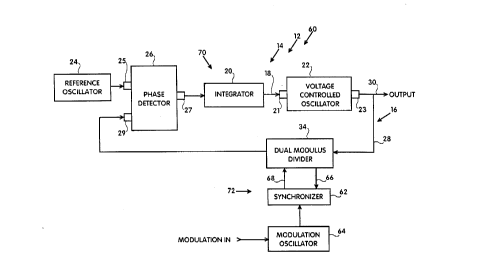
Referring now to FIGURE 6, in a third embodiment of the present
invention, an electrical device, or D.C. modulated phase locked oscillator,
100 includes like-named and like-numbered components as described in
10 conjunction with FIGURES 1-4.
The electrical device 100 of FIGURE 6 produces a crystal
referenced output that is D.C. modulated, as has been described for the
FIGURE 5 embodiment, and the device 100 provides substantially
simultaneous modulation of both the forward path 14 and the Feedback
15 path 16, also as described for the FIGURE 5 embodiment.
In addition, the electrical device 100 of FIGURE 6 provides
channelization of the output frequency as well as D.C. modulation of the
output frequency.
Both D.C. modulation and channelization of the output frequency .
are achieved by controlling the dual modulus divider 34 by two separate
means.
More particularly, channelization is achieved by controlling the
dual modulus divider 34 by the variable modulus divider 48 and the
modulus controller 50 in the integrated chip 42; and D.C. modulation is
achieved by controlling the dual modulus divider 34 by the modulation
oscillator 64.
The function of the synchronizer 62 of FIGURE 4 is achieved in
FIGURE 6 by a synchronizer 101 which consists of first and second flip-
flops, 102 and 104, and by an OR gate 106.
When a cycle, or pulse removing signal, is delivered to a clock
terminal 108 of the flip-flop 102 by the modulation oscillator 64, an
output terminal, or Q terminal, 110 is energized, thereby energizing an
input terminal, or D terminal, 112 of the flip-flop 104. The pulse
removing signal from the modulation oscillator 64 is held by the flip-
flop 102 until the flip-flop 102 is reset by a signal to a reset terminal
114.
~,
isn
Assuming that the dual modulus divider 34 has been dividing
the feedback signal in the feedback path 16 by one or the other of the
dividing ratios, when the dual modulus divider 34 has finished
16
performing a dividing operation which is done to achieve channelization,
a pulse in a conductor 116 is directed to a clock terminal 118 of the
flip-flop 104 and to the modulus controller 50 of the integrated chip 42.
With energizing of the clock terminal 118, a modz.tlus control
signal is sent from a Q terminal, or output terminal, 120 of the flip-flop
104 to the dual modules divider 34 via the OR gate 106 and a conductor
122, thereby changing the dividing ratio of the dual modules divider 34
from the lower dividing ratio to the higher dividing ratio for one
dividing cycle, and thereby removing one pulse from the feedback path
16.
Completion of the next dividing cycle sends a signal in the
conductor 116 to the modules controller 50; and the modules controller
50 sends a reset signal to a reset terminal 124 of the flip-flop 104 via
a conductor 126, and sends a modules control signal to the dual modules
divider 34 via the conductor 126, the OR gate 106, and the conductor
122.
Also, as a signal is sent from the Q terminal 120 of the flip-
flop 104 to the OR gate 106 and to the dual modules divider 34, a reset
signal is sent; from the Q terminal 120 of the flip-flop 104 to the reset
terminal 114 of the flip-flop 102, thereby resetting the flip-flop 102.
Thus, it can be seen f;hat; a synchronizer 62, consisting of the
flip-flops, 102 and 104, and the OR gate 106, cooperates with the
modules controller 50 to prevent; simultaneous control of the dual
modules divider 34 by the variable modules divider 48, which provides
channelization of the output frequency. and simultaneous control oP the
dual modules divider 34 by the modulation oscillator 64 which provides
D.C. modulation of the output frequency of the elect;rical device 100.
It should be understood that. in the FIGlIRE 6 embodiment, the
electrical device, or D.C. modulat;ed phase locked oscillator, 100 includes
a phase locking oscillator 128 for producing a phase locked output, and
a D.C, modulator 130 for D.C. modulating the output frequency of the
phase locking oscillator 128.
Also, it should be understood that the phase locking oscillator
128 of the FIGURE 6 embodiment includes the phase locked loop 12 with
both the forward path 14 and the feedback path 16, the voltage
controlled oscillator 22, the operational amplifier 52 and the capacitor 54
which cooperate to provide the integrator 20, the prescaling divider 36,
the crystal 46, and the integrated chip 42.
"...
17
The portions of the integrated chip 42 that are included in the
phase locking oscillator 128 are: the reference oscillator 44 which
cooperates with the crystal 46 to provide the crystal controlled reference
oscillator 24, the phase detector 26, the variable modulus divider 48,
and the modulus controller 50.
Finally, it should be understood that the modulator 130 of the
FIGURE 6 embodiment includes the dual modulus divider 34, the flip-
flops, 102 and 104, which cooperate with the OR gate 106 to function as
the synchronizer 62 of FIGURES 4 and 5, and the modulation oscillator
64, all of which are operatively connected to the feedback path 16. The
modulator 130 of FIGURE 6 also includes the summing resistors, 82 and
84, and the modulation conductors, 86 and 88.
As stated above, the dual modulus divider 34 is a part of the
modulator 130; but also, the dual modulus divider 34 is a part of the
phase locking oscillator 128 as the dual modulus divider 34 cooperates
with the variable modulus divider 48 and the modulus controller 50 to
provide channelizatfon of the phase locking oscillator 128.
Referring now to FIGURE 7, in a fourth embodiment of the
present invention, an electrical device, or D.C. modulated phase locked
oscillator, 140 includes a shift register 142 in a synchronizer 143 in
addition to the flip-flops, 102 and 104. Further, the synchronizer 143
of the FIGURE 7 embodiment includes the OR gate 106, an AND gate 144,
and an inverter 146.
More specifically, the shift register 142 includes the flip-flops,
102 and 104, for achieving the synchronizing functions, and any desired
number of flip-flops 148 which cooperate with each other to remove more
than one pulse from the feedback path 16 for each cycle of the
modulation oscillator 64.
Thus, the shift register 142 provides means for removing a
plurality of pulses from the feedback path 16 for each cycle of the
modulation oscillator 64. Therefore, the shift register 142 allows the
frequency of the modulation oscillator 64 to be relatively low for a
given range of frequency modulation of the output, and yet allows the
frequency of the crystal controlled reference oscillator 24 to remain
relatively high, thereby assuring rapid phase locking together with an
adequate range of frequency modulation.
Further, the shift register 142, in allowing the frequency of the
modulation amplifier to be quite low, keeps the frequency drift of the
d~-,
y ~3 ~~ Lt ._
~~~~~'
18
modulation oscillator 64 extremely low, so that the combined drift of the
modulation oscillator 64 and the crystal controlled reference oscillator 24
are only a fraction of prior art designs.
The operation of the electrical device, or D.C. modulated phase
locked oscillator, 140 of FIGURE 7 differs from the operation of the
FIGURE 6 embodiment primarily in the multiple pulse removing of the
shift register 142, and in circuitry that is added to inhibit a clock
terminal 150 of t;he shift register 142 when there is conflict between
control of the dual modulus divider 34 by the modulus controller 50, and
control of the dual modulus divider 34 by the shift register 142.
More particularly, the clock terminal 150 of the shift register
142 is inhibited by the AND gate 144 and the inverter 146 from
receiving a signal from the conductor 116, except when a signal provided
by the inverter i 46 in a conductor 152 is applied t.o the AND gate 144
simultaneously with a signal. in the conductor 116 from the dual modulus
divider 34.
It should be understood that, in the FIGiJRE 7 embodiment, the
D.C. modulated oscillator 140 includes a phase locking oscillator 154 for
producing a phase locked output, and a D.C. modu.lator 1.,56 for D.C.
modulating the output frequency of the phase locking oscillator 154.
Also, it should be understood that the phase locking oscillator
154 of the FIGURE 7 embodiment includes the phase locked loop 12 with
both the forward path 14 and the feedback path 16, the voltage
controlled oscillator 22, the operational amplifier 52 and the capacitor 54
which cooperate to provide the integrator 20, t;he crystal 46, and the
integrated chip 42.
Portions of the integrated chip 42 that are included in the
phase locking oscillator 154 are the reference oscillator 44 which
cooperates with the crystal 46 to provide the crystal controlled reference
oscillator 24, the phase detector 26, the variable modulus divider 48,
and the modulus controller ,50.
Further, it should be understood that the modulator 156 of the
FIGURE 7 embodiment includes the dual modulus divider 34, the shift
register 142 which cooperates with the OR gate 106, the AND gate 144,
and the inverter 146 to function as the synchronizer 62 of FIGURES 4
and b, and the modulation oscillator 64, all of which are operatively
connected to the feedback path 16. The modulator 156 of FIGURE 7 also
19
includes the summing resistors, 82 and 84, and the modulation
conductors, 86 and 88.
The dual modulus divider 34 functions as a part of the
modulator 156 to achieve D.C. modulation of the output frequency, and
also functions as a part of the phase locking oscillator 154 to provide
channelization of the phase locking oscillator 154.
Referring now to FIGURE 8, an electrical device, or D.C.
modulated phase locked oscillator, 160 includes components generally as
named, numbered, and described in conjunction with the embodiment of
FIGURE 6.
However, the electrical device 160 of FIGURE 8 does not include
the prescaling divider 36, the dual modulus divider 34, the flip-flop 104,
the integrated chip 42, or the OR gate 106 of the FIGURE 6 embodiment.
Instead, the electrical device 160 of FIGURE 8 includes an
integrated chip 162, a flip-flop 164, a resistor 166, and a diode 168.
The integrated chip 162 is of the type manufactured by Motorola under
the number 45151 which is shown in FIGURE 12. The integrated chip
162 includes the reference oscillator 44, the phase detector 26, and the
variable modulus divider 48, all of which function as described for the
integrated chip 42. The flip-flop 164 includes a D input terminal 170, a
Q output terminal 172, a Not-Q output terminal 174, and a clock
terminal 176.
The flip-flops 102 and 164 and the modulus controller 50
cooperate to function as a synchronizer 62 for the embodiment of FIGURE
8, as shown by the following description.
In operation, when the flip-flop 164 is in the unclocked state,
the Not-Q output terminal 174 is "high", and the diode 168 prevents
this "high" from reaching a feedback conductor 178, so that all pulses
from the output conductor 30 are fed back to the integrated chip 162.
However, when the modulation oscillator 64 produces a pulse, the
flip-flop 102 is clocked, thereby producing a "high" at the output
terminal 110 which is delivered to the input terminal 170 of the flip-
flop 164. When the next pulse from the output conductor 30 and the
feedback conductor 28 is applied to the clock terminal 176 of the flip-
flop 164, the flip-flop 164 fs clocked to the state wherein the Q output
terminal 172 is "high" and the Not-Q output terminal 174 is "low". With
the Not-~ output terminal 174 "low", the pulse delivered to the feedback
conductor 28 is pulled down by the resistor 166 and the connection of
19/1
the conductor 178 to the "low" of the Not-Q output terminal 174 via the
diode 168.
A
20 ~ ~~'
At substantially the same time, the flip-flop 164, being clocked
by the output pulse at the clock terminal 176, delivers a "high" from the
output terminal 172 to the reset terminal 114 of the flip-flop 102,
thereby resetting the flip-flop 102 for receiving the next pulse from the
modulation oscillator 64.
Therefore, for each pulse of the modulation oscillator 64, one
pulse is removed from the feedback path 16. That is, one pulse is
dissipated, or prevented from reaching, the integrated chip 162; and the
phase detector 26 cooperates with the integrator 20 to increase the
output frequency of the voltage controlled oscillator 22 to increase the
output frequency by one Hertz.
It should be understood that the electrical device 160 includes a
phase locking oscillator 180 and a D.C. modulator 182. The phase
locking oscillator 180 includes the voltage controlled oscillator 22, the
crystal controlled reference oscillator 24, the phase detector 26, and the
variable modulus divider 48. The D.C. modulator 182 includes the
modulation oscillator 64, the flip-flops 102 and 164, the resistor 166,
the diode 168, and the resistors 82 and 84. Further, the flip-flops, 102
and 164, cooperate with the diode 168 and the resistor 166 to provide a
synchronizer 184.
Referring now to FIGURE 9, an electrical device, or D.C.
modulated phase locked oscillator, 190 includes components generally as
named, numbered, and described in conjunction with the embodiment of
FIGURE 6.
However, the electrical device 190 of FIGURE 9 does not include
the OR gate 106 of the FIGURE 6 embodiment. Instead, the electrical
device 190 of FIGURE 9 includes the resistor 166 and the diode 168 of
FIGURE 8.
The flip-flops 102 and 104 and the modulus controller 50
cooperate to function as a synchronizer 62 for the embodiment of FIGURE
9, as shown by the following description.
In operation, when the flip-flop 104 is in the unclocked state,
the diode 168 blocks current flow to the output terminal 120; and the
circuitry functions as described for FIGURE 6.
However, when the modulation oscillator 64 produces a pulse, the
flip-flop 102 is clocked, producing a "high" at the output terminal 110
and energizing the input terminal 112 of the flip-flop 104. Then, when
the dual modulus divider 34 finishes a division by one of the dual
~, ~~ ~ '~ 1'
. 20/1
dividing ratios, it delivers a pulse to the conductor 116, clocking the
flip-flop 104.
With the flip-flop 104 clocked, a "high" is produced at the
output terminal 120 of the flip-flop 104; and this high at the output
' 21
terminal 120 is used to reset flip-flop 102 in preparation for another
pulse from the modulation oscillator 64.
In addition, this high from the output terminal 120 is delivered
to the conductor 178, making the conductor 178 "high". With the output
terminal 120 connected to the conductor 178 through the diode 168, and
with the resistor 166 being interposed between the conductors 178 and
116, the conductor 178 is kept "high" as the conductor 116 goes "low"
between pulses.
The result is, by preventing a "low" in the conductor 178
between two pulses delivered to the conductor 116 by the dual modulus
divider 34, two pulses are combined into one; and in effect, one pulse is
removed from the feedback path 16 in the conductor 178.
Removing one pulse from the conductor 178 effectively removes a
number of pulses from the feedback path 16 that is equal to the
dividing ratio of the prescaling divider 36 times the lower dividing ratio
of the dual modulus divider 34.
For instance, if the prescaling divider 36 has a dividing ratio of
16, and if the lower dividing ratio of the dual modulus divider 34 is 20,
then each pulse of the modulation oscillator 64 removes 16 times 20, or
320 pulses from the feedback path 16. Therefore, to increase the output
of the voltage controlled oscillator 22 by 10 MHz, the required frequency
of the modulation oscillator 64 would be 31,250 Hertz.
Notice that in this manner extremely wide frequency deviations
can be achieved. This is, of course, at the expense of increased drift
since the modulation oscillator drift is multiplied by the ratio shown
above, that is, 320. In the example shown, a typical drift of 30 kHz at
the output could be caused by the drift of the modulation oscillator 64
when multiplied by 320. This drift is still well within the drift allowed
from transmitters which would use this wider deviation capability.
The electrical device 190 of FIGURE 9 provides a much greater
frequency deviation for a given frequency of the modulation oscillator 64
than does the electrical device 140 of FIGURE 7, since a counter or a
shift register, such as the shift register 142, removes only a small
number of plurality of pulses from the feedback path 16 for each pulse
of the modulation oscillator 64. More specifically, if the shift register
142 removes 10 pulses from the feedback path 16 for each cycle of the
modulation oscillator 64, the electrical device 190, in removing 320
pulses from the feedback path 16 for each cycle of the modulation
s,
,~ ~ ,
22
oscillator 64, removes 32 times as many pulses from the feedback path
16 for each cycle of the modulation oscillator 64.
Further, as previously noted, since the frequency drift of a
voltage controlled oscillator, such as the modulation oscillator 64, is
smaller, as a percentage of output frequency, for lower frequencies, the
total drift of the D.C. modulated oscillator 190 as described herein is
less when a plurality of pulses are removed from the feedback path 16
for each cycle of the modulation oscillator 64, and the frequency of the
modulation oscillator 64 is reduced.
The pulse removal, or pulse combining, as described in
conjunction with FIGURE 9, must be prohibited when the dual modulus
divider 34 is in the higher mode to prevent an incorrect output
frequency. To prevent the pulse removing function from removing a
pulse resulting from division at the higher dividing ratio, the conductor
126 is connected to the flip-flop 104 in addition to being connected to
the dual modulus divider 34. This connection of the conductor 126 to
the flip-flop 104 provides synchronization of the modulating and dividing
functions as described previously.
It should be understood that the electrical device 190 of FIGURE
9 includes a phase locking oscillator 192 and a D.C. modulator 194. The
phase locking oscillator 192 includes the voltage controlled oscillator 22,
the crystal controlled reference oscillator 24, the phase detector 26, the
variable modulus divider 48, and the modulus controller 50. The D.C.
modulator 194 includes the modulation oscillator 64, the flip-flops 102
and 104, the resistor 166, the diode 168, and the resistors 82 and 84.
A synchronizer 196 of the FIGURE 9 embodiment includes the flip-flops,
102 and 104, the resistor 166, and the diode 168. The synchronizer 196
cooperates with the modulus control conductor 126 to provide the
synchronizing function, as described previously.
Referring again to FIGURE 6, if the dual modulus divider 34 were
set so that the normal state were to divide at the higher dividing ratio,
' rather than normally to divide at the lower dividing ratio, then, in
effect, one pulse would be added to the feedback path 16, rather than
removed therefrom.
That is, if the dual modulus divider 34 were dividing by a
dividing ratio of 21, and then dividing at the ratio of 20 once per
second, the frequency in the feedback path 16, as supplied to the phase
detector 26, would be increased by one pulse per second; and the phase
u.
.~..
22/1
detector 26 and the integrator 20 would cooperate with the voltage
controlled oscillator 22 to reduce the output frequency by one Hertz.
Of course, to obtain an increase in the output frequency as a
function of the frequency of the modulation oscillator 64, with the
A
r3 F~ ~~ ce ~s
y ..? ,-'
E"
23
dividing ratios inverted as noted above, would require providing an
inverted I).C. modulation voltage t:o the modulation oscillator 64, while
continuing to supply an uninverted D.C. modulation voltage to the
resistor 84.
It is important to notice that D.C. modulation of a phase locked
loop is achieved in the present invention by either removing pulses from
the feedback path 16 or adding pulses to the feedback path 16.
Removal of pulses is achieved by increasing the dividing ratio of
the dual modules divider 34 once for each cycle of the rn.odulation
oscillator 64 as shown in FIGURE 6, by increasing the dividing rat3.o a
plurality of times for each cycle of the modulation oscillator 64 as
shown in F1GIJRE 7, by removing a very large number of pulses from the
feedback path 16 when both the 1>rescaling dividor 36 is included and
one output pulse is eliminated, as shown in FIGURE 9, or by removing
16 many pulses from the feedback path 16 by eliminating one output pulse
from a circuit In which either the dual modules divider 34 or the
prescaling divider 36 is included.
Removal of pulses, or elimination of pulses, is achieved by
preventing a "high" from passing though the resistor 166 of FIGURE 8,
thereby removing a pulse by dissipating it through the resistor 166 to a
"low" of the Not-Q output terminal 174.
Also, removal of pulses is achieved by preventing a "low" from
appearing in the conductor 178 of FI<JURE 9 by placing a "high" in the
conductor 178 from the output terminal 120, through the diode 168, and
into the conductor 178, while isolating the "high" in the conductor 178
from a "low" in the conductor 116 by the resistor 166 for one cycle.
Or, stated more broadly, the use of the resistor 166 and the
diode 168 prevents a change in the signal level in the feedback path 16.
In FIGURES 4 and 5, the synchronizer 62 is shown symbolically.
In the FIGURE 6 embodiment, the synchronizer 62 includes the flip-flops
102 and 104, the OR gate 106, and the modules controller 50 of the
integrated chip 42. In the FiGIJRE 7 embodiment, the synchronizer 62
includes the flip-flops 102 and 104, the OR gate 106, the AND gate 144,
the inverter 146, and the modules controller 50. In the FIGURE 8
embodiment. the synchronizer 62 includes the flip-flops 102 and 164.
And, in the FIGURE 9 embodiment, the synchronizer 62 includes the flip-
flops 102 and 104, and the modules controller 50.
",~
' 24
Referring now to FIGURE 10, a radio frequency receiver, or signal
processing apparatus, 200 comprises an input stage 202 an I.F. stage
203, a demodulator 204 that includes both the I.F. stage 203, an rf
mixer 210, and the phase locking oscillator 128 of FIGURE 6, and the
6 modulator 130 of FIGURE 6.
The input stage 202 includes an rf preselector 206 and an rf
amplifier 208; and the I.F. stage 203 includes an I.F. amplifier/filter 212,
a local mixer 214, and a local oscillator 216.
More particularly, the input stage 202 is connected to a first
input 213 of the rf mixer 210, the phase locking oscillator 128 is
connected to a second input 215 of the rf mixer 210, and the I.F.
amplifier/filter 212 of the I.F. stage 203 is connected to an output 217
of the rf mixer 210.
In operation, the input stage 202 receives and amplifies an rf
input signal that is frequency modulated; the phase locking oscillator
128 generates a phase locked signal, that is, a signal that is phase
locked to a crystal controlled reference frequency; the amplified rf signal
is mixed with the phase locked signal in the rf mixer 210, and
demodulated in the LF. stage 203 to produce a demodulated output signal
in an output conductor 218. That is, the D.C. modulator 130 uses the
output signal in the output conductor 218 to D.C. modulate the phase
locked signal. Therefore, the signal in the output conductor 218 is the
demodulated output.
The rf input signal may be in the 2200 to 2400 MHz range, the
D.C. modulated phase locked oscillator 100 may have an output frequency
in the range of 1700-1900 MHz, and the local oscillator 216 may have a
frequency of 500 MHz. However, these frequencies are given merely as
an example. In actual practice, the input frequencies may be in any
range of rf frequencies, or even in frequencies that are below the rf
range, and that are connected to the receiver 200 by other means, such
as electrical connection or light waves.
For purposes of understanding the claims, it should be recognized
that the signal processing apparatus 200 of FIGURE 10 includes the
electrical device 100 of FIGURE 6.
More particularly, it should be recognized that the circuitry of
the radio frequency receiver 200 includes the phase locking oscillator
128 and the D.C. modulator 130, both of FIGURE 6.
A
' 24/1
Referring again to FIGURE 4, for purposes of understanding the
claims, the following should be observed: The output 27 of the phase
detector 26 controls the integrator 20, the integrator 20 controls the
VCO 22, and the VCO 22 produces the output frequency in the output
conductor 30. Because of this forward progression of control, as opposed
to feedback of the output signal from the output conductor 30 to the
input 29 of the phase detector 26, as used in the appended claims, the
forward path 14 of the phase locked loop 12 includes: the phase detector
26, the integrator 20, the forward path conductor 18, the VCO 22, and
the output conductor 30.
In like manner, since the output signal feeds back from the
output conductor 30 to the input 29 of the phase detector 26 as a
feedback signal, as used in the appended claims, the feedback path 16
includes the feedback conductor 28 and the dual modulus divider 34.
Since the phase detector 26 provides an output which is a
function of the difference between the phase angle of the feedback
signal to the input 29 and the reference frequency in the input 25, the
phase detector 26 is a part of the forward path 14.
It follows that the electrical components of the other
embodiments of the present Invention can be understood to be a part oP
the forward path 14, to be a part of the feedback path 16, or to be a
part of neither one, in accordance with the flow of signal from the phase
detector 26 toward the output conductor 30, or the flow of signal from
the output conductor 30 back to the phase detector 26.
For instance, it is evident that the prescaling divider 36 of
FIGURE 5 is in the feedback path 16. In like manner, referring to
FIGURE 6, the output conductor 30, the prescaling divider 36, the dual
modulus divider 34, and the A and N counters of the variable modulus
divider 48 of the integrated chip 42 are a part of the feedback path 16.
However, it is obvious that the reference oscillator 44 of the integrated
chip 42 is not a part of the forward path 14, nor a part of the feedback
path 16; because it is outside the loop l2.Further, it should be
recognized that each of the electrical devices 60, 80, 140, 160, and 190
of FIGURES 4, 6, 7, 8, and 9 includes a phase locking oscillator 70, 90,
154, 180, or 192, respectively, for producing a phase locked output; and
each of the electrical devices 60, 80, 140, 160, and 190 of FIGURES 4, 5,
7, 8, and 9 includes a modulator 72, 92, 156, 182, or 194, respectively,
i.
v i
24/2
for D.C. modulating the output of the phase locking oscillator 70, 90,
154, 180, or 192, respectively.
A
25
Therefore, any of the oscillators and modulators of FIGURES 4, 6,
7, 8, or 9, or any other components that provide the same functions, can
be substituted for the phase locking oscillator 128 and the D.C.
modulator 130 which are shown in FIGURE 10.
While the present invention has been described with particular
components, it should be understood that the scope of the present
invention is to be determined by the terminology used in the claims, and
by the functions recited therein, without regard to more specifically
described components in the detailed description.
Further, while examples have been given for frequencies, it
should be understood that the present invention will function as
described, and is useful in the gigahertz range, in the megahertz range,
in the kilohertz range, and below the kilohertz range. For this reason,
frequency limiting terms, such as radio frequency, are not needed, nor
16 included, in the claims.
While specific apparatus and method have been disclosed in the
preceding description, it should be understood that these specifics have
been given for the purpose of disclosing the principles of the present
invention and that many variations thereof will become apparent to
those who are versed in the art. Therefore, the scope of the present
invention is to be determined by the appended claims.
Industrial Applicability
The present invention is applicable to phase locked oscillators,
voltage controlled crystal oscillators, single frequency transmitters and
receivers, channelized transmitters and receivers, telemetry and video
transmitters such as are used for commercial, consumer, and military
products, and to all such electrical devices in which low frequency drift,
inclusion of a maximum number of channels within a limited frequency
range, large frequency deviations, and/or rapid synchronization to
modulation frequencies are/is required, whether the output frequencies be
in the gigahertz range, in the megahertz range, in the kilohertz range, or
even lower than the kilohertz range.