Note: Descriptions are shown in the official language in which they were submitted.
Z034356
Background of the Invention
This invention relates to idling systems for
operating a device at a reduced speed when no load is
applied to the device. More particularly, this
invention relates to an idling system for use with a
device that also has a speed control system.
Speed control systems that cause devices such
as power producing, transferring and absorbing machines
to operate at a fixed speed when a load is electrically
connected to the machine are well known in the art.
Such speed control systems are commonly referred to as
~speed governors~. Such speed governors typically are
either of the mechanical type or of the electronic
type.
~5 Various types of mechanical qovernors are
well known in the art. When a load is typically
applied to a power producing device such as an internal
combustion engine having a simple mechanical governor,
the speed or RPM of the engine decreases significantly
below the no load speed. To reduce speed droop upon
loading, the sensitivity of mechanical governors may be
increased. However, as the mechanical sensitivity of
the governor is increased, the engine and control
mechanism tend to become unstable.
Electronic speed governors are also well
known in the art. Such electronic devices permit more
accurate control of engine speed and minimize engine
- speed droop with load while at the same time decreasing
engine instability.
Electronic speed controllers or governors are
known which operate the device at a fixed speed or RPM
when a load i8 applied, but cause the device to be
operated at a different or lower speed as soon as the
load i8 electrically disconnected from the device. The
problem with such idlers is that continuous cycling may
.. ..
-: ~- ,. . ..
,.
..... .
''' ^
.... .. .
203A356
occur between the higher governed speed and the idle
speed if the load is intermittently applied to the
device for brief periods of time. For example, in the
construction industry a generator device may be used to
power a drill or other construction equipment. The
drill or other equipment may be used intermittently by
the worker; it may be operated for a few seconds or a
few minutes, then stopped for a few seconds, and then
operated again. Since the generator that powers the
drill or load is constantly operating, it will cycle
between the governed speed and the lower idle speed if
the idler takes over as soon as the load is
disconnected from the generator.
Summarv of the Invention
~5 An idling system is disclosed for use with
devices that power loads, where the device also has a
speed control means such as a governor for adjusting
the speed of the device, and where the device also has
a load sensing means that senses whether a load is
~ applied to the device.
The idling system includes a disable means
for outputting a disable signal to the speed control
means. The disable signal disables the speed control
means after a predetermined time delay period when the
load sensing means senses that no load is then applied
to the device. The idling system also includes a time
delay means for delaying the outputting of the disable
signal to the speed control means for a predetermined
time delay period 80 that the device may be started and
to minimize cycling between the governed speed and the
idle speed. An activation means may also be included
for activating the speed control means by disabling the
disable means when the load sensing means senses that a
load is then applied to the device.
:
203~356
In a first embodiment, the time delay means
includes an input means for receiving a periodic signal
representative of at least one revolution of the device
and a first capacitor that is charged by the periodic
S signal. The disable means includes a first switch that
is activated when the first capacitor is charged and
which outputs the disable signal.
Also in a first embodiment, the activation
means includes a full wave rectifier that rectifies a
~0 load sensing signal generated by said load sensing
means, a second capacitor that is charged by the
rectified load sensing signal, and a second switch that
is activated when the second capacitor is charged. The
first capacitor thereafter discharges to deactivate the
~5 first switch, thereby preventing the disable means from
outputting the disable signal to the speed control
means. The first embodiment of the idling system may
also include a conditioning means for conditioning the
load sensing signal, and a resistor connected to the
first capacitor that enables the first capacitor to
fully discharge after the device stops operating.
In a second embodiment, the disable means
includes an AND gate whose inputs are the inverted load
sensing signal and the output from the time delay
means. In the second embodiment, the time delay means
lncludes first and second pluralities of frequency
dividers which frequency divide down a clock signal and
output a positive-going, frequency divided signal after
a time delay period to the AND gate. When both the
inverted load 8ensing signal is high-indicating that no
load is applied-and the output signal from the time
delay means is high, the AND gate outputs a disable
signal to disable the engine's speed control means.
The second embodiment also includes a
8tarting means for disabling the disable means during
. . .
.. -: .. . . . , -........... , .
,: . , : ..;
. . ..
_4- X03~3S6
engine starting, thereby allowing the engine to reach a
predetermined minimum RP~I before the idling system is
operable. The starting means includes a counter that
counts engine revolutions and outputs a low speed
signal when the speed of the device is below the
predetermined minimum speed. The starting means also
includes an OR gate that has the low speed signal and
the load sensing signal as inputs.
It is a feature and advantage of the present
invention to provide an idling system for use with
devices such as internal combustion engines which have
electronic governors.
It is another feature and advantage of the
present invention to provide an idling system with a
time delay to reduce cycling of the device speed
between the higher governed speed and the lower idle
speed.
It is yet another feature and advantage of
the present invention to provide a low cost idling
8ystem which may be retrofit onto a device having an
electronic governor.
It is yet another feature and advantage of
the present invention to provide an idling system which
automatlcally begins operation after engine start-up
without manual intervention.
These and others features and advantages of
the pre~ent invention will be apparent to those skilled
in the art from the following detailed description and
the drawings of the preferred embodiments, in which:
30Brief Description of the Drawinq
FIG. 1 is a schematic drawing of a first
embodiment of the present invention.
FIG. 2 is a flow diagram of a second
embodiment of the present invention.
-5- 2~343~
FIGS. 3A and 3s together comprise a schematic
diagram of the second embodiment of the present
invention. FIG. 3A is the left hand side of the
schematic, and FIG.3B is the right hand side.
Detailed Descri tion of the Preferred Embodiment
P
The idling system according to the present
invention is described herein in connection with
internal combustion engines. However, the present
description is for illustrative purposes only, and the
idling system of the present invention may also be used
with various types of power producing, transferring and
absorbing devices. For example, it may also be used to
regulate or control the speed of electric motors,
electric generators, clutches, brakes, and continuous
variable transmissions.
The idling system according to the present
invention is designed to be used with devices having a
speed controller or electronic governor. One suitable
governor i8 disclosed in U.S. Patent No. 4,875,448
issued October 24, 1989 to Richard A. Dykstra and
assigned to Briggs & Stratton Corporation, the assignee
of the present invention.
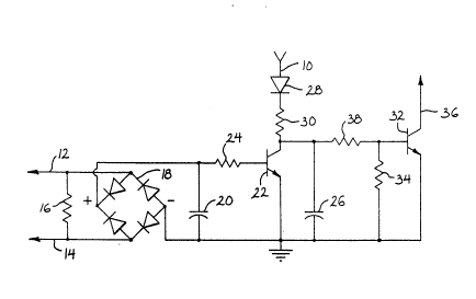
Referring now to FIG. 1, a periodic square
wave signal is input to the idling system by input
means 10. The periodic signal is preferably related to
the speed of the device, and may represent one or more
revolutions of the device. The periodic signal may be
derived from a timer in the device's electronic speed
control circuit. If the idling system of the present
invention is used with the governor disclosed in U.S.
Patent No. 4,875,448, the periodic signal input to
input means 10 may correspond to the output from timer
1 (not shown) of the '448 patent. Alternatively, the
.::
- ,, -~
-6- 2034356
input periodic signal may be derived from an alternator
winding if an alternator is used on the internal
combustion engine, or from an alternator powered by an
internal combustion engine. Other sources of the-input
periodic signal may be used.
In FIG. 1, leads 12 and 14 are connected to a
load sensing toroid coil (not shown) which is wound
around the generator's power lead wire if the idling
system is used in a generator. The purpose of the load
sensing toroid is to sense whether a load is applied to
t~e device. If a load is so applied, a load sensing
voltage signal is developed across the load sensing
toroid. Resistor 16 connected across the toroid acts
as a filter to help limit electrical noise across the
toroid. The diode bridge 18, along with second
capacitor 20, develop a DC voltage to bias on second
transistor switch 22 through resistor 24.
When no load is sensed by the load sensing
means or when the engine is being started, periodic
signals input by input means 10 pass through diode 28
and resistor 30 and charge first capacitor 26 since the
second switch, transistor 22, is then off. When
capacitor 26 becomes sufficiently charged, first switch
32 begins to conduct. The turning on of the disable
means, transistor 32, causes a disable signal to be
generated on line 36 connected to the power
semiconductor device of the speed controller. If the
speed controller is the one described in U.S. Patent
No. 4,875,448, the po~er semiconductor device
corresponds to power transistor 58 (not shown) which
controls the engine throttle positioner, solenoid 59
~not shown) as described in the '448 patent.
In the alternative, the disable signal could
be used to reset the counters in an electronic
governor, or it could turn on a solenoid to override a
mechanical governor.
.
--7--
~03~3S6
The fact that the idling system according to
the present invention uses the power transistor and
throttle positioner solenoid of the device's electronic
governor enables the idling system to be sold without
those components. This reduces the overall cost of the
idling system, and allows the idling system to be
retrofit onto devices having a suitable speed control
circuit.
Also, the embodiment depicted in FIG. 1 is an
~ automatic idling system in that it is engaged without
manual operator intervention. That is, no manual
switch is needed to activate the idling system after
the engine is cranked as is required in other idling
systems.
The disable signal generated by transistor 32
along line 36 is a low voltage signal which is lower
than the voltage signal applied to the speed
controller's power semiconductor device. Other types
of disable signals could be used. The low voltage
signal causes the control voltage signal of the speed
controller's power semiconductor device to be reduced
to the value of the collector-emitter voltage of
transistor 32. As a result, the speed controller's
throttle positioner is de-energized, and a throttle
return spring (not shown) brings the device down to a
low idle speed since the power semiconductor device's
control voltage then becomes too low to sustain
conduction through the power semiconductor device.
The time delay means, including input means
10 and first capacitor 26, delays the outputting of the
di~able signal. The time delay means preferably
imposes a five to fifteen second delay between the time
that the engine i8 first cranked or the load is
disconnected from the device and the outputting of the
disable signal which disables the device's speed
',;. !. ' ' ' ' ' ' '
. ~,. - ' '
,
', , - '- ' ' , ' "' "'.
' ' ~,.,, "
'' ''' ' :''.
': ': ' ' . ": ' ''
-8- 2034~S6
controller. This time delay increases the chance that
the engine will start by allowing the engine to operate
at speeds higher than the idle speed during starting.
When the engine is running, this time delay lessens the
number of cyclings between the higher governed speed
and the idle speed caused by the intermittent
application and disconnection of the load to the
device.
When a load is applied to the device, an
activation means activates the speed controller by
disabling the disable means. The activation means
includes diode bridge 18, second capacitor 20, second
transistor switch 22, and resistor 24.
When a load is applied, the load sensing
voltage signal is rectified by full wave bridge
rectiier 18 and charges second capacitor 20. When the
voltage becomes sufficiently high the rectified and
filtered load sensing signal is applied to the base of
second transistor 22 through resistor 24, thereby
activating or turning on transistor 22. When second
transistor 22 is activated by being turned on, first
capacitor 26, which had been charged through diode 28
and resistor 30 by the periodic signal, discharges
immediately through the collector-emitter junction of
transi~tor 22. The base-emitter junction of first
transistor 32 then becomes too low to sustain
conduction, and the first switch, transistor 32, is
turned off.
The turning off of first transistor 32
dlsables the di~able means consisting of first switch
32, causing the outputt~ng of the disable signal to
cease. When first transistor 32 is activated by being
turned on, it outputs the disable signal to the
devlce's speed control means.
9 2034356
The cessation of the disable signal allows
the speed contoller's power semiconductor device to be
activated, causing the speed controller to operate the
engine at its fixed, higher governed speed.
When the load is thereafter removed from the
engine, first capacitor 26 must once again charge
before first transistor 32 is able to conduct, so that
a brief time delay of five to fifteen seconds occurs
before the engine returns to its lower idle speed.
Resistor 34 allows capacitor 26 to become completely
discharged after operation of the device has stopped,
thus completely resetting the idling system.
FIG. 2 is a flow diagram of a second
embodiment of the present invention. As can be seen
from FIGS. 2, 3A and 3B, the second embodiment employs
digital circuitry whereas the first embodiment depicted
in FIG. 1 uses analog components. However, the second
embodiment uses a load sensing means similar to that
discussed in connection with FIG. 1, as long as the
load sensing means used with the second embodiment
outputs a 5 volt DC load sensing signal when a load is
present.
The operation of the second embodiment will
be discussed in connection with FIG. 2. In FIG. 2, a 1
MHz input signal i~ input via input 40 to a first
plurality of frequency dividers 42. Although it is
a88umed that a 1 MHz input clock signal is used, a wide
range o alternate input frequencies could be used.
The clock signal may be input from the timer in the
eng1ne's speed controller, or from any other oscillator
8uch as a readily available, inexpensive, accurate
crystal oscillator.
The first plurality of frequency dividers 42,
whlch correspond to the row of flip flops on the left
hand side of FIG. 3A, divide the 1 MHz input clock
'
- . . ,; ' ' ' ,, ' , ' .
., ~ . . . : ~
- 1 o- 2034356
signal by 4,096 to yield a 244 Hz signal. The 244 Hz
signal is output to a second plurality of frequency
dividers 44, corresponding to the row of flip flops in
FIG. 3B. Although the second embodiment of the present
invention uses flip flops as divide-by-two frequency
dividers, it is apparent that other types of frequency
dividers could be used. Indeed, the frequency dividers
could be eliminated altogether if the input clock
signal had a low enough frequency so that the timing
delay pulse signal of appropriate duration would be
output without further frequency division.
In FIG. 2, the second plurality of frequency
dividers 44 divides the 244 Hz output from frequency
dividers 42 by 4,050 to yield an 8.3 second delay
lS pulse. That is, the output from frequency dividers 44
will go to its low state for 8.3 seconds and thereafter
to its high state. The output from frequency dividers
44 i8 input to AND gate 46 via line 48. The other
input of AND gate 46 is obtained from the output of
load sensing means 50, which output is inverted by
inverter 52. The inverted load sensing signal is input
to AND gate 46 via line 54. Another multiple input
gate such as a NAND, OR or NOR gate could be used in
place of AND gate 46 with suitable changes in the
circuit.
AND gate 46 outputs a disable signal via line
56 to electronic governor 62 only when both of its
inputs are positive-going pulses. The inputs to AND
gate 46 are both positive only when no load is sensed
by load sensing means 50 and when the timing delay
signal has ended. In other words, when no load is
sensed by load sensing means 50, the electronic
governor 62 will not be disabled until an 8.3 second
time delay period has passed. The delay period
minimizes cycling between the lower idle speed and the
. .
-
- 1 1 - 2034356
higher governed speed when a load is intermittently
applied to the device. No such cycling will occur
until 8.3 seconds have passed.
The delay period of 8.3 seconds was chosen
S for illustrative purposes; other delay periods could be
used and still be within the scope of the present
invention. However, the desired range of time delay
periods is typically between about five and fifteen
seconds. The length of the time delay period could be
changed by choosing a different frequency clock signal
and/or a different number or combination of frequency
dividers 42 and 44.
The second embodiment also includes a
starting means consisting of a counter 64 and an OR
gate 66. The function of the starting means is to
disable the load sensing means 50 while the engine
speed is less than a predetermined number of
revolutions per minute. In the second embodiment,
counter 64 determines whether the time between
successive ignition pulses is greater than 65
milli8econds. A time period of 65 milliseconds between
successive ignition pulses corresponds to an engine
speed of 915 RPM. In effect, the starting means
disables the load sensing means and the disable means
when the engine speed i8 less than about 915 RPM,
thereby allowing the engine to reach this predetermined
~peed before the idling system is operable. Other
predetermined minimum engine speeds could be chosen by
varying the desired time, as determined by counter 64,
between successive ignition pulses.
When the engine is being started, no load is
preeent. Thus, the idling system would normally be
operable to di~able the electronic governor 62 and
return the engine speed to idle speed after an 8.3
8econd delay. However, the starting means is used in
..; . , .
, ,., : : :, -
..
.' ' '; , . :
.... - . . ...
-12-
Z0343~6
place of the time delay period during engine
starting. When the time period between successive
ignition pulses is greater than 65 milliseconds,
counter 64 outputs a positive-going pulse to the input
of OR gate 66 as depicted in FIG. 2. Holding this
input of OR gate 66 high effectively disables the load
sensing means 50 and the disable means as discussed
below.
The positive-going pulse input to OR gate 66
causes second reset 68 to reset the second plurality of
frequency dividers 44. The resetting of frequency
dividers 44 causes the output transmitted along line 48
to the input of AND gate 46 to go low, causing the
output of AND gate 46 along line 56 to governor 62 to
be zero. Thus, governor 62 is operable so that the
engine runs at the higher governed speed until the
engine reaches the predetermined minimum RPM, and the
idling system is then inoperable.
After the minimum engine RPM is reached,
counter 64 outputs a negative-going signal to the input
of OR gate 66, so that the output of 0~ gate 66 and the
r4setting of frequency dividers 44 via second reset 68
depends exclusively on whether a load is sensed by load
sensing means SO. If a load is sensed by load sensing
means 50, the output of OR gate 66 goes positive,
causing reset 68 to reset frequency dividers 44. The
resetting of dividers 44 causes the dividers to output
a negative-going pulse to AND gate 46. AND gate 46
then cannot output a disable signal, thus allowing the
governor 62 to control the engine speed when a load is
present.
When no load is present and when the engine
speed exceeds the minimum engine RPM, load sensing
mean~ 50 and counter 64 both output negative-going
pulses to OR gate 66, 80 that the output of OR gate 66
., .
-13- 203~356
is negative-going. The second reset 68 does not reset
frequency dividers 44. Thus, counters which comprise
frequency dividers 44 will count down, causing the
output of the time delay means to go positive after the
time delay period. The AND gate 46 then outputs a
disable signal via line 56 to electronic governor 62
since the AND gate also receives the positive, inverted
load sensing signal as an input. The electronic
governor will then be disabled, and the engine will
return to its lower idling speed.
The first plurality of frequency dividers 42
is reset by a first reset 70. Reset 70 outputs a
positive-going 4 millisecond pulse every other engine
revolution to reset frequency dividers 42.
As with the first embodiment depicted in FIG.
~5 1, the disable signal output by AND gate 46 could be
used to ground the base of the governor's power
transistor, to reset the counters in the electronic
governor, or to turn on a solenoid to override a
mechanical governor.
FIGS. 3A and 3B together comprise a schematic
diagram of the second embodiment of the present
invention. The schematic depicted in FIGS. 3A and 3B
correspond to the flow chart depicted in FIG. 2
diRcu~sed above. In FIG. 3A, the first plurality of
frequency dividers 42 is comprised of flip flops 42a.
Each of flip flops 42a is a model 4013 dual type D CMOS
flip flop such as that manufactured by Motorola under
Part No. MC14013B. Each of the devices 42a actually
consist~ of two flip flops or divide-by-two frequency
dividers.
Similarly, the second plurality of frequency
dividers 44 depicted in FIG. 3B consists of a plurality
of flip flop frequency dividers 44a, each of which is a
model 4013 device like dividers 42a.
,
.. : ' ' - ,,, . : I
,~
.
...... ," .,.,., ,,,, ., ,, ~ ..... ..... . .
-14- Z034356
Counter 64 (FIG. 3A) used to generate the 915
RPM reference signal is also a model 4013 flip flop
except that counter 64 is connected such that only one
of the flip flops is utilized.
Although the idling system of the present
invention may be used with a wide variety of devices,
it is particularly suitable for generators powered by
internal combustion engines having a rating of up to 24
horsepower. It may be used with larger generators as
well. It is particularly suitable for use with small
generators used in the construction industry to power
tools such as drills and the like.
Although preferred embodiments of the present
invention have been shown and described, other
alternate embodiments will be apparent to those skilled
in the art and are within the intended scope of the
present invention. Thus, the present invention is to
be limited only by the following claims.
,"~
.
, .. . ~,. ~