Note: Descriptions are shown in the official language in which they were submitted.
r
-1-
15XZ03254
APPRATOS AND METHOD READING DATA FROM
A SOLID STATE X-RAY DETECTOR
The present invention relates to X-ray systems utilizing
a solid state multiple element X-ray detector for producing an
image; and more particularly, to techniques for reading the
signals from the detector elements and processing the signals.
Conventional fluoroscopy equipment includes a source for
projecting an X-ray beam through an object to be analyzed, such
as a medical patient. After the beam passes through the
patient, an image intensifier typically converted the X-ray
radiation into a visible light image, and a video camera
produced an analog video signal from the visible image for
display on a monitor. Because an analog video signal was
produced, much of the image processing for automatic brightness
control and image enhancement Was performed in the analog
domain.
Recently, high resolution solid state X-ray detectors
have been proposed, which comprise a two dimensional array of
3,000 to 4,000 photo diode detector elements in each dimension.
Each element produces an electrical signal which corresponds to
the brightness of a picture element in the X-ray image
projected onto the detector. The signal from each each
~~~~~ 6~~
-2- 15XZ03254
detector element is read out individually and digitized for
further image processing, storage and display.
The high resolution provided by such a large array of
detector elements may be beneficial to the analysis of the
patient in many certain circumstances. However, in situations
where a high degree of resolution is not required, the
processing of the incumbent large amount of data from the array
significantly increases the image processing time above that
which is reasonably required. Furthermore, certain X-ray
systems may not require a detector with such a high degree of
resolution in which case a smaller matrix detector would be
satisfactory. However, in this instance it may be cost
effective to still utilize the larger matrix detector, rather
than develop a different size detector for each piece of X-ray
equipment having a different resolution requirement. In both
these cases when the detector produces a higher resolution
image than is required, a technique for reducing the amount of
data is desirable.
A problem inherent in conventional photo diode detector
arrays is that the biasing charge placed on the photo diode may
be partially discharged by transistor current leakage and by a
mechanism commonly known as "dark current". The charge
depletion due to the effects of dark current and current
leakage produces an offset of the image signal. Since the
amount of charge removed'by these currents is not constant, the
~0~~~~~~.
_3_ 15XZ03254
signal offset varies, adding a element of uncertainty to the
detector output.
The amount of charge removed from the photo diode by
these currents in part is a function of the length of time from
photo diode biasing until detector element c!:arge sensing. As
a consequence, it is desirable to minimize the time required to
read out the elements of the detector array in order to
minimize the effect of these currents. This presents a trade-
off in that it is also desirable to increase the readout time
in order to reduce the bandwidth of the image signal processing
circuit and reduce the electrical noise added to the detector
signal by the circuit.
Summary of the Invention
A solid state image sensor is formed by a two dimensional
array of photodetectors arranged in m columns and n rows, where
m and n are integers. For high resolution image sensing, the
array can have approximately 4000 photodetectors in each column
and row. The photodetectors in each column are connected to a
common column output line by a separate switch means. The
switch means for the photodetectors in each row are activated
by a signal on a common row select line.
The image data sensed by each photodetector is read out
by activating the row select lines in a given sequence.
-4' 15XZ03254
Initially, a group of one or more row select lines near the
middle of the array are activated to apply signals from the
associated photodetectors to the column output lines. Then a
similar group of row select lines on one side of the middle are
activated to couple signals from its associated photodetectors
to the column output lines. Another similar group of one or
more row select lines on the other side of the array middle is
activated to apply signals from its corresponding
photodetectors to the column output lines. In the preferred
embodiment, signals from the remaining rows of photodetectors
are readout by alternately activating row groups on opposite
sides of the middle of the array.
When the groups consist of a plurality of rows the
signals from photodetectors in several rows along each column
are combined into the signal on the column output line. This
produces a data reduction along one dimension of the array and
of the image being sensed, In order to achieve symmetry in the
data reduction to avoid image distortion, circuitry external to
the image sensor combines the signals from a plurality of
column output lines. Ideally the number of such output line
signals to combine is chosen so that the image following data
reduction has the same aspect ratio as the image prior to data
reduction.
-5- 15XZ03254
An object of the present invention is to provide a
technique for reducing the amount of picture elements in an
image.
Another object is to provide a method for reading image
data from the central portion of the array and then
progressively reading the image data outward from the array
center. Such an outward scan reduces the deterioration of the
central image portion due to effects that are a function of the
elapsed time between image exposure and readout.
A further object is to provide a technique and apparatus
for varying the degree of image data reduction depending upon
the amount of image resolution required in the resultant image.
FIGURE 1 is a block diagram of an X-ray fluoroscopy
system utilizing the present invention;
FIGURE 2 is a schematic diagram of the image detector
array in the system of Figure 1;
FIGURE 3 is a schematic diagram of an alternative image
detector array for the system of Figure 1;
FIGURE 4 illustrates a digital data reduction circuit for
processing the picture elements from the detector array; and
FIGURE 5 is an alternative analog data reduction
circuit.
_6_ 15XZ03254
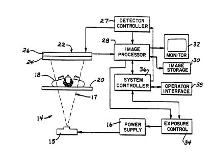
With initial reference to Figure 1, an X-ray apparatus 14
includes an X-ray tube 15 Which, when excited by a power supply
16, emits an X-ray beam 17. As illustrated, the X-ray beam is
directed toward a patient 18 lying on an X-ray transmissive
table 20. The portion of the beam Which is transmitted through
the table and the patient impinges upon an X-ray detector
designated 22. The X-ray detector 22 comprises a scintillator
24 that converts the X-ray photons to lower e:.~yy photons in
the visible spectrum. Contiguous with the scincillator 24 is a
photodetector array 26, which converts the lig'.-.~ photons into
an electrical signal. A detector controller 27 contains
electronics for operating the detector array to acquire an
image and to read out the signal from each photodetector
element.
The output signal from the photodetector array 26 is
coupled to an image processor 28 that includes circuitry for
processing and enhancing the X-ray image signal. The processed
image then is displayed on a video monitor 32 and may be
archived in an image storage devise 30. The image processor 28
additionally produces a brightness control signal which is
applied to an exposure control circuit 34 to regulate the power
supply 16 and thereby the X-ray exposure.
-7- 15XZ03254
The overall operation of the X-ray apparatus 14 is
governed by a system controller 36 which receives commands from
the X-ray technician via an operator interface panel 38.
Figure 2 illustrates the circuitry of the photodetector '
array 26, which is formed by a matrix of detector elements 40.
i
The detector elements 40 are arranged on an amorphous silicon
wafer in a conventional two-dimensional array of m columns and
n, rows, where m and n are integers. For example, a typical i
high resolution X-ray detector is a square array of 3,000 to
4,000 rows and columns of elements.
Each detector element 40 includes a photo diode 42 and a
thin film transistor 44. The photo diodes 42 are fabricated
from a large wafer area ensuring that the photo diode will
intercept a sizeable portion of the light produced by the
scintillator 24. Each photo diode 42 also has a relatively
large capacitance that allows it to store the electrical charge
resulting from the photon excitation.
The cathode of the photo diodes 42 in each column of the
array is connected by the source-drain conduction path of the
associated transistor 44 to a common column signal line (48'1
through 48'm~ for the column. For,example the photo diodes 42
in column 1 are coupled to the first signal line 48-1, The
anodes of the diodes in each row are connected in common to a
source of a negative bias voltage (-V). The gate electrodes of
the transistors 44 in each row are connected to a common row
N0344'~~
_8._ 15XZ03254
select line (46-1 through 46'°,~ such as line 46'1 for row 1.
The row select lines and the column signal lines are coupled to
the detector controller 27 and the column signal lines also are
connected to the image processor 28.
In order to acquire an X-ray image using the detector
illustrated in Figure 2, the apparatus 14 performs the
following sequence of operations. Initially, the detector
controller 27 connects all the column signal lines 48'1 through
48'm to ground, and applies a positive voltage (Von) to all the
row select lines 46-1 through 46'n. The positive voltage
applied to the row select lines turns on the transistor 44 in
each detector element 40 placing a positive charge on the
reverse biased photo diodes 42. Once the photo diodes have
been fully charged, the detector controller 27 applies a
negative voltage (-Voff), which is more negative than the
negative supply voltage (-V), to the row select lines 46'1
through 46'n. This negative biasing of the row select lines
turns off the transistor 44 in each detector ele.~.,ent 40.
Then the detector 22 is exposed to a pulse of X-ray
photons produced in a conventional manner by the system
exciting tube 15 to generate a beam 17 of X-ray photons. The
X-ray photons are converted to lower energy photons by the
scintillator 24. When these lower energy photons strike the
photo diodes 42 in the detector 26, the diodes conduct
electricity and discharge~a portion of their positive charge.
a
~~~44~11
15XZ03254
The amount of the positive charge removed from a given photo
diode 42 depends upon the amount of lower energy photons which
strikes it, which in turn depends upon the intensity of the X-
ray energy that strikes region of the scintillator 24 adjacent
to the photo diode. Therefore, the amount of charge removed
from the photo diode 42 in each detector element 40 is a
function of the X-ray intensity striking the corresponding
region of the X-ray detector 22.
After the termination of the X-ray exposure, the residual
charge in each photo diode 42 is sensed. To do so, the column
signal line 48'1 through 48-m for each detector array column is
simultaneously connected to separate sensing circuits in the
image processor 28. Any of several types of sensing circuits
can be incorporated into the image processor 28. Fe:- example,
the sensing circuit can measure the voltage across the photo
diode, and therefore the amount of charge remaining on the
photo diode. Alternatively, the sensing circuit can connect
the associated column signal line 48'1 through 48-m to ground
potential and measure the amount of charge that is r~~.~:ired to
replace the charge removed by the X-ray exposure.
For maximum image resolutiop, the photo diode charges
are sensed a row at a time by the detector controller 27
sequentially applying the positive voltage Von to each of the
row select lines 46-1 through 46-n. When a row select line is
positively biased, the detector array transistors 44 connected
~~~z~~~~~~
-10-
15XZ03254
to that row select line are turned on thereby coupling the
associated photo diodes 42 in the selected row to their column
signal lines 48-1 through 48-'".
In order to decrease the amount of time required to read
out the signal from each detector element in the array, the
rows of detector elements can be divided into two groups, as
illustrated in Figure 3. In this example for a detector array
26 with n rows, the detector elements 40' in row 1 through row
n/2 are connected to a first group of column signal lines 47.
Similarly, the detector elements 40" in row (n/2)+1 through row
n are connected to a second group of column signal lines 49.
In this example, the detector elements 40' in the top half of
the array can be read out simultaneously with the detector
elements 40" in the bottom half in the array. It should be
noted that this alternative embodiment of the detector array 26
requires twice the number of signal sensing circuits. However,
the time required to sense the charge in the detector elements
is decreased by a factor of two; or alternatively, the sensing
time can be the same as with the previous embodiment allowing
the bandwidth of the sensing circuits to be reduced. In
addition, the subdivision of the detector array reduces the
electrical noise and capacitance seen by the sensing circuits.
As noted above, in applications where the full resolution
of the detector array 26 is not required, it is advantageous to
reduce the amount of image data. With the X-ray detector 22,
-11- 15XZ03254
the detector elements can be combined along the rows a.nd the
columns in order to reduce the number of picture elements.
With a two-dimensional image, the data reduction must occur
equally in both dimensions in order to avoid distorting the
resultant image. To produce a variety of fields of view, image
matrix sizes and image acquisition rates, the present system is
able to subdivide the image into two-dimensional groups of q
by p detector elements where p and q are an integers. The q
by p groups have the same aspect ratio as the entire array.
For the exemplary square array p and q are equal, having a
common value in the range from 1 to 4 for example. This
results in subdivision groups having 1, 4, 9 or 16 detector
elements.
In a variation of the present concept, the detector array
does not comprise a square matrix of detector elements. For
example, there may be more columns of detector elements than
rows in the array, such as in imagers for an NTSC standard
video camera. Although a non-square detector array is used,
the image processing may require a square array of image data.
In such a case, the signals from the detector elements in the
extra columns either are not used~or are combined it~~ a square
matrix of image elements. When this is done, the non-square
detector array becomes equivalent to a square one insofar as
the present concept is concerned. With this variation, the
variables m and n may not represent the number of columns and
~~s~~~~~
-12- 15XZ03254
rows of detector elements in the actual detector array but
rather m and n correspond to the number of columns and rows in
the equivalent square array.
Referring again to Figure 2, the charge signals from
adjacent detector elements 40 can easily be combined along a
column by simultaneously applying the positive voltage Von to a
group of row select lines 46-1 through 46-n. In this case, if
the sensing circuits measure the voltage from the photo diodes
42 on the column signal lines 48'1 through 48-m, the output of
each sensing circuit will correspond to the average of the
signals from the selected group of detector elements in the
corresponding array column. On the other hand, if the sensor
circuits measure the current required to replace the charge
removed from the photo diodes 42, the output of each sensing
circuit will correspond to the sum of the signals from the
selected group of detector elements in the column.
While signals from the detector elements 40 in several
rows can be combined by simultaneously selecting several rows
in the array, combining the signals from detector elements in
adjacent columns (i.e. along the other dimension of the array)
must be accomplished by external circuitry. With reference to
Figure 4, a sensing circuit 50 is'incorporated into the image
processor 28 to combine the signals from multiple columns.
This circuit 50 allows detector elements to be sensed
individually or combined.into 2, 3 or 4 columns. The portion
r,.~~~~f~~
-13- 15X203254
of the sensing circuit 50 for the first twelve columns of
detector elements 40 is illustrated in Figure 4. Replicas of
this circuit portion are provided for each group of twelve
adjacent array columns.
The sensing circuit comprises a series of modules 51, 52,
53 and 54, with each module processing the output signals from
three columns of the array. The first module 51 is coupled to
the column signal lines 48'1, 48'5 and 48'9 for columns 1, 5,
and 9 of the detector array 26; and module 52 is coupled to the
column signal lines 48'2, 48'6 and 48'1 for columns 2, 6 and
10. Similarly, the third module 53 receives the detector array
column signal lines 48'3, 48'~ and 48'11 for columns 3,7 and 11;
and the fourth illustrated module 54 is coupled to column
signal lines 48'4, 48'8 and 48'12 for columns 4,8 and 12 of the
detector array.
The internal circuitry of each module 51-54 is identical
and the circuitry for the first module 51 shall be described in
detail. The column signal lines 48'1, 48'9 and 48'5 for
columns 1,5 and 9 are each coupled to the input of a separate
integrator 56. The output from each integrator 56 is connected
to a sample and hold circuit in an analog to digital converter
(ADC) 58, which samples the output of the integrator and
converts the output into a digital form. The separate
digitized outputs are stored in three sets of data buffers 60.
The digital output from each set of data buffers 60 in the
~4 ~ ,5 ~~ Lk f
-14- 15XZ03254
module 51 are connected to separate inputs of a four-to-one
multiplexes 62 (MLJX A). The data lines for the fourth input to
multiplexes 62 are all coupled to ground potential to provide
an input representing the number zero.
The multiplexers 62 for each of the four illustrated
modules 51, 52, 53 and 54 are designated as MUX A, MUX B, MC1X C
and MUX D, respectively. The outputs from the four
multiplexers 62 in modules 51-54 are coupled to inputs of an
adder circuit 64 to produce the sum of the multiplexes outputs,
as indicated by the arithmetic expression A+B+C+D within the
adder block. Therefore, the output from the adder circuit 64
represents the summation of the signals from each of the module
multiplexers 62; and the combination of the image signals from
a group of detector array columns..
Although not illustrated in Figure 4, the multiplexers 62
in the sensing circuit 50 receive control signals from the
detector controller 27 directing each multiplexes to couple one
of the input lines to its output line. Depending upon the
control signal applied to the four multiplexers A, B, C and D
in each in a group of four modules 51-54, the output signals
from 1, 2, 3 or 4 columns of detector elements 40 can be
combined into the output from the adder 64 for that group of
modules.
To select a single column, the associated mult'_plexer 62
is directed to couple the corresponding input line to its
~~y.~~ 9~~~
-15-~ 15XZ03254
output line and each of the other multiplexers for the group of
four modules 51-54 is directed to couple the grounded fourth
input to their respective output lines. This action produces a
summation in adder 64 of the selected column signal with zero
signals from the other multiplexers 62. For example to select
i
only the second column, multiplexes B is directed to couple its
first input to its output and multiplexers A, C and D are
directed to couple their fourth inputs to their outputs. I
Thereafter, a different set of directions can be sent to the
multiplexes 62 to sequentially access the signals from each of
the other column signal lines from the detector array. Since
i
each column is being addressed individually by the technique,
no reduction of the image data occurs.
To achieve the maximum amount of data reduction available
from this circuit, the image data on four signal lines of the t
I
detector array 26 are combined by sensing circuit 50. For
example, when the signals for columns 1-4 are to be combined,
the four multiplexers 62 are all directed to couple their first ~
input to their outputs. This action applies the signals from
column signal lines 1, 2, 3 and 4 to the inputs of adder 64
where they are summed and sent to, the adder's output. Then,
I
sequentially, each adjacent group of four columns of the
detector array 26 can be processed by changing the directions
sent to the multiplexers so that the signals from other module I
buffers 60 are sequentially combined by the adder 64.
-16- 15XZ03254
From the above description, one skilled in the art can
easily understand how to utilize the sensing circuit 50 and
direct the multiplexers 62 to produce a data reduction by
combining detector elements in pairs or trios of adjacent array
columns.
The circuit disclosed in Figure 4 employes a separate
analog-to-digital converter 58 for each column signal line 48-1
through 48-m from the detector array 26. This has the
advantage of enabling the use of converters with relatively
slow digitization rates, but requires a relatively large number
of converters. As an alternative, the data may be combined
before digitizing, thus reducing the number of analog to
digital converters. However, in this alternative, faster
converters will have to be utilized, and the potential for the
introduction of electronic noise in the analog combining
circuitry is increased.
An example of such a alternative sensing circuit 70 is
shown in Figure S. As with the original embodiment of a
sensing circuit 50 in Figure 4, the alternative circuit 70 is
illustrated for twelve columns of the detector array with the
understanding that replicas of this circuit portion are
provided for each group of twelve adjacent array columns. This
portion of the signal sensing circuit 70 is formed by four
modules 71, 72, 73 and 74 as denoted by the dashed lines in the
drawing. Each module 72-74 receives three of the column signal
17 15XZ03254
lines which are coupled to separate integrators 76. The output
from the three integrators 76 within a module are coupled to
separate inputs of an analog four-to-one multiplexer 77. The
fourth input of the analog multiplexer 77 is coupled to ground
potential to provide a zero potential input. Each multiplexer
77 can set its output to any of the three input signals from
the detector array or to the grounded input. The outputs from
the four module multiplexers MUX A, MLJX B, MtJX C and MUX D then
are combined in a summing amplifier 78. The summation of the
signals from the four modules 71-74 is digitized by an
analog-to-digital converter (ADC) 80, and the result is stored
in a digital buffer 82. Figure 5 also shows the detector
controller 27, which provides control signals to the sensing
circuit 70 as illustrated.
The multiplexers 77 within each module 71-74 are directed
in a similar manner to that described with respect to the
operation of sensing circuit 50 in Figure 4, to individually
access each column signal line or combine pairs, trios, or
quartets of column signal lines in order to achieve the desired
degree of data reduction.
When the X-ray system is aligned with the patient, the
area of the patient's body which is of primary interest
typically is placed at the center of the X-ray system's field
of view. Therefore, the central picture elements of the X-ray
image will be of primary. importance to the medical personnel
-18- 15XZ03254
using the system. To ensure the best image quality of the
center of the image, the present invention minimizes the time
which elapses from pre-charging the photo diodes until the rows
of picture elements at the center of the detector array 26 are
scanned for charge readout. This is accomplished by sensing
the central rows first and sequentially selecting rows on
alternate sides of the center which are progressively farther
and farther from the center of the array. This minimizes the
elapsed time for the central image elements.
The tables in the Appendix contain the sequence in which the
detector element rows are selected for each of the two
embodiments of the detector array illustrated in Figures 2 and
3 and for different degrees of data reduction.
With respect to the photodetector array illustrated in
Figure 2, for example, Table I illustrates the sequence in
which the detector controller 27 activates each of the row
select lines 46'1 through 46'n to read out the charge on
individual photo diodes 42. As illustrated in the table during
the first readout period, the detector controller 27 applies
the positive voltage (Von) to the row select line, designated
n/2, at the center of the detector array. This enables the
charge in each of the photo diodes of this central row to be
read out on their corresponding column signal line 48'1 through
48'm. Since no data reduction is occurring in this example,
only one row at a time is selected by the detector controller
r
x
15XZ03254
-19-
27. After sufficient time has elapsed for the sensing circuits
in the image processor 28 to measure the remaining charge on
each of the diodes, the detector controller 27 applies the
negative voltage minus Voff to the central row select line n/2.
Then the detector controller selects one of the row
select lines which is immediately adjacent to the central one,
which is designated row (n/2)+1, by applying a positive voltage
Von to the next row select line. Once the charges in the photo
diodes for that row have been sensed, the detector controller
applies the -Voff voltage to the (n/2)+1 row select line.
Then, the detector controller 27 chooses the row select line on
the other side of the central row, Which line is designated as
(n/2)-1, and in a similar manner, energizes that line to sense
the charges on the row's photo diodes.
As seen in Table I the next two rows selected designated
(n/2)+2 and (n/2)-2 are two rows removed from the center of the
array. This sequence of row selection continues until finally
the first and last rows have been selected for charge sensing.
When the data reduction technique is to be applied during
the readout of the photodetector charges, a plurality of row
select lines are turned on simultaneously depending upon the
degree of data reduction desired.
As shown in Table II, the data is reduced by selecting
two rows of the detector array 26 during each readout period.
During the first readout period, the detector controller 27
-20-
15X203254
chooses the central row (n/2) and one of the adjacent rows
(n/2)-1 of the detector array 26. Since when two rows are
selected, two photo diodes in each column of the array will
have their charges applied to the corresponding signal lines 48
so that the signal on each of these lines 48 represents the
charge in two photodetector sites 42. As each pair of rows is
being read out, the sensing circuit in Figure 4 is operated to
combine the signals from pairs of adjacent columns of the
detector array 26 as previously described. These combined
signals are further processed for display on monitor 32 and
storage in device 30 (see Figure 1).
At the completion of the first readout period of the data
reduction technique illustrated in Table II, another pair of
adjacent rows on one side of the middle of the photodetector
array 26 are selected and their charges similarly read out in a
combined manner. In the third readout period, the next
adjacent pair of rows on the opposite of the middle of the
photodetector array 26 are chosen by the detector controller 27
activating their row select lines. The readout process
continues with the detector controller 27 selecting adjacent
pairs of photodetector array row's alternating on either side of
the middle of the array and moving farther and farther away
from the middle. Eventually, the first and second rows will be
chosen and their charges,read out, followed by ~-;~e ultimate and
penultimate rows in the final readout period. As illustrated
1. .x.
-21- 15XZ03254
by the comparison of Tables I and II, the data reduction
technique in the latter example, in which pairs of rows are
read out simultaneously, has hal:E the number of readout periods
as in the Table I example in which each photodetector array
site is read out individually.
Similar data reduction techniques occur in the examples
depicted in Tables III and IV. Table III relates to a readout
scheme in which the data is reduced through the simultaneous
readout of trios of rows and similarly combining trios of
columns in the sensing circuit 50 illustrated in Figure 4. The
data may be reduced even more by the technique depicted in
Figure 4 in which quartets of rows are simultaneously read out
by simultaneously activating four row select lines 46 during
each readout period.
Tables V through VIII depict the readout techniques
utilized with the photodetector array illustrated in Figure 3
where each column of photodetector elements 40 is divided in
half with the upper group of photo elements being connected to
a separate column signal line from the lower group of detector
elements. With this photodetector array structure, when the
detector elements are to be read out individually, a row in the
upper half and a row in the lower half of the array is read
simultaneously. As depicted in Table V during the first
readout period, the two rows (n/2) and (n/2)+1 at the center of
the array are selected by the detector controller 27. During
'22- 15XZ03254
the next readout period, the next adjacent rows (n/2)-1 and
(n/2)+2 on either side of the array center are selected. The
selection continues until the first and last rows are selected
during the final readout period.
When the data read out of the detector array in Figure 3
is to be reduced, two rows in both the top and bottom sections
of the array can be read during each readout period. The row
readout for this data reduction technique is illustrated in
Table VI. Similarly, when the data in this detector array is
to be reduced further, three rows in both the upper and lower
sections of the detector array 26 are simultaneously read by
the detector controller 27 activating six row select lines
during each readout period as depicted in Table VII. Table
VIII provides the readout scheme when the data from the
detector array in Figure 3 is to be reduc=d even further. In
this case, eight rows are activated simultaneously by the
detector controller 27 with four of those rows being in the
upper half and the other four in the lower half of the detector
array 26.
-23-
15XZ03254
Row selection sequence to sense individual X-ray detector
elements in the embodiment in Figure 2.
Readout Row
pAriod Selected
1 (n/2)
2 (n/2) +1
3 (n/2) -1
4 (n/2) +2
(n/2) -2
n-1 1
n n
Row selection sequence to sense X-ray detector elements
grouped by pairs of rows in the embodiment in Figure 2.
Readout Rows
1 (n/2) and (n/2) -1
2 (n/2)+1 and (n/2)+2
3 (n/2) -2 and (n/2) -3
4 (n/2)+3 and (n/2)+4
(n/2)-1 ~ 2 and 1
(n/2) n-1 and n
-24-
15XZ03254
Row selection sequence to sense X-ray detector elements
grouped by Trios of rows in the embodiment in Figure 2.
Readout Rows
1 (n/2), (n/2)-1 (n/2)-2
and
2 (n/2) +1, (n/2) +2 (n/2)
and +3
3 (n/2)-3, (n/2)-4 (n/2)-5
and
4 (n/2)+4, (n/2)+5 (n/2)+6
and
(n/3) -1 3, 2 and 1
(n/3) n-2, n-1 and n
Row selection sequence to sense X-ray detector elements
grouped by quartets of rows in the embodiment in Figure 2.
Readout Rows
1 (n/2) , (n/2) -1, (n/2) -2 (n/2>
and -3
2 (n/2)+1, (n/2)+2, (n/2)+3 (n/2)+4
and
3 (n/2) -4, (n/2) -5, (n/2) -6 (n/2)
and -7
4 (n/2) +5, (n/2) +6, (n/2) +7 (n/2)
and +S
(n/4)-1 4, 3, 2 and 1
(n/4) n-3, n-2, n-1 and n
-2g_
15XZ03254
Row selection sequence to sense X-ray detector elements
individually in the embodiment in Figure 3.
Readout Rows
~
i
~
od
(n/2) and (n/2)
+1
(n/2)-1 and (n/2)+2
(n/2)-2 and (n/2)+3
(n/2)-3 and (n/2)+4
(n/2)-1 2 and n-1
(n/2) 1 and n
Row selection sequence to sense X-ray detector elements
grouped by pairs of rows in the embodiment in Figure 3.
Readout Rows
ari nri Sel
1 (n/2) , (n/2) -l, (n/2) (n/2)
+1 and +2
(n/2) -2, (n/2) -3, (n/2) (n/2)
+3 and +4
(n/2) -4, (n/2) -5, (n/2) (n/2)
+5 and +6
(n/2)-6, (n/2)-7, (n/2)+7 (n/2)+8
and
(n/4)-1 4, 3, n-3 and n-2
(n/4) 2, 1, n-1 and n
2~3~4~1
-2fi-
15XZ03254
Row selection sequence to sense X-ray detector elements
grouped by trios of rows in the embodiment in Figure 3.
Readout Rows
period
S lp~~ d
1 (n/2), (n/2)-1, (n/2)-2, (n/2)+1, (n/2)+2 and (n/2)+3
2 (n/2) -3, (n/2) -4, (n/2) -5, (n/2) +4, (n/2) +5 and (n/2) +6
(n/2 ) -6, (n/2) -7, (n/2) -8, (n/2) +7, (n/2) +g and (n/2) +9
4 (n/2)-9, (n/2)-10, (n/2)-11, (n/2)+10, (n/2)+11 and (n/2)+12
(n/6) -1 6, 5, 4, n-5., n-4 and n-3
fn/6) 3, 2, 1, n-2, n-1 and n
Row selection sequence to sense X-ray detector elements
grouped by quartets of rows in the embodiment in Figure 3.
Each line of this table represents a different readout period.
Bow Selection for n/a
(n/2), (n/2)-1, (n/2)-2, (n/?)-3, (n/2)+1, (n/2)+2, (n/2)+3 and (n/2)+4
(n/2)-4, (n/2)-5, (n/2)-6, (n/2)-7, (n/2)+5, (n/2)+6, (n/2)+7 and (n/2)+8
~.6, 5,n-7,n-6 n-5 and
n-4
4,3,2, 1,n-3,n-2, n-1
and n