Note: Descriptions are shown in the official language in which they were submitted.
--`` 2~34481
SELF-ALIGNE~ GATE PROCESS FOR FABRICATING
. FIELD EMIT~ER ARRAYS
1 BACKGROUND
The present invention relates generally to field
emitter arrays, and more particularly to a process for
fabricating self-aligned micron-sized field emitter arrays.
Recently there has been considerable interest in
field emitter arrays for reasons discussed by H. F. Gray et
al. in "A Va~uum Field Effect Transistor Using Silicon
Fleld Emitter Arrays", IEDM, 1986, pages 776-779. Field
emitter arrays typically comprise a metal/insulator/metal
fllm sandwich with a cellular array of holes through the
upper metal and insulator layers, leaving the edges of the
upper metal layer (which serves as an accelerator
electrode) effectively exposed to the upper surface of the
lower metal layer ~whlch ~erves as an emitter electrode).
A number of conically-shaped electron emitter elements are
mounted on tho lowor metal layer and extend upwardly
therefrom such that thelr respective tips are located in
respoctlve holes in the uppor metal layer. If appropriate
voltages are applled between the emitter electrode,
_/,
203~481
1 accelerator electrode, and an anode located above the
accelerator electrode, electrons are caused to flow from
the respective cone tips to the anode. Further details
regarding these devices may be found in the papers by C. A.
Spindt, "A Thin-Film Field-Emission Cathode", ~ournal of
Applied Physics, Vol. 39, No. 7, June 1986, pages
3S04-3505, C. A. Spindt et al., ~Physical Properties of
Thin-Film Field Emission Cathodes with Molybdenum Cones",
Journal of AD~lied Phvsics, Vol. 47, No. 12, December 1976,
pages 5248-5263, and C. A. Spindt et al., "Recent Progress
in Low-Voltage Field-Emission Cathode Development", ~ournal
de Physioue, Vol. 45, No. C-9, December 1984, pages
269-278, and in U.S. Patent No. 3,453,478 to K. R.
Shoulders et al. and U.S. Patents Nos. 3,665,241 and
3,755,704 to C. A. Spindt et al. Additional patents
disclosing methods for fabricating field emitter array
devices are U.S. Patent No. 3,921,022 to J. D. Levine, U.S.
Patent No. 3,998,678 to S. Fukase et al., U.S. Patent
4,008,412 to I. Yuito et al., U.S. Patent No. 4,307,507 to
H. F. Gray et al., and U.S. Patent No. 4,513,308 to R. F.
Greene et al.
In the conventional approaches to fabrication of
$ield emitter arrays, precise alignment and hole size
control has been very difficult to achieve, because of the
very 6mall geometries and tolerances in the devices.
Typically, in order to obtain precise alignment, it has
been necessary to employ a difficult~and time-consuming
ma~k 6tep to insure proper alignment and formation.
Accordingly, it would be advantageous to have a
proce~fi of fabricating field emitter arrays that was
selr-aligning and that is les~ difricult and costly to
implement.
2034481
SUMMARY OF THE INVENTION
In order to provide for an improved process by which
to form field emitter arrays, the present invention
fabricates the arrays in accordance with the following
process steps. Substantially conical field emitter
elements are formed on a surface of a substrate, after
which a layer of oxide is deposited on the substrate
surface and over the field emitter elements. A layer of
metal is then deposited over the layer of oxide to form a
gate metal layer. A layer of photoresist is then deposited
over the gate metal layer.
The layer of photoresist is then plasma etched in an
oxygen atmosphere to cause portions of the photoresist
above respective field emitter elements to be removed and
thereby provide self-aligned holes in the photoresist over
each of the field emitter elements. The exposed gate metal
layer above the field emitter elements is then etched using
the layer of photoresist as a mask. The photoresist layer
is removed, and the layer of oxide is etched to expose the
field emitter elements.
In addition, further processing may be performed to
provide a second oxide layer and an anode metal layer in
field emission triode devices.
Other aspects of this invention are as follows:
A process for fabricating a field emitter array,
said process comprising the steps of;
forming substantially conical field emitter elements
on a surface of a substrate;
depositing a layer of oxide over said substrate
sur~ace and said field emitter elements;
depositing a layer of metal over said layer of oxide
to form a gate metal layer;
depositlng a layer of photoresist over said gate
metal layer;
2034481
3a
plasma etching said layer of photoresist in an
oxygen atmosphere to cause portions of photoresist above
respective field emitter elements to be removed and
thereby expose respective portions of said gate metal
layer above respective tip regions of said field emitter
elements;
etching the exposed portions of said gate metal
layer using said layer of photoresist as a mask;
removing said layer of photoresist; and
etching the exposed portions of said layer of oxide
to expose said field emitter elements.
A process for fabricating a field emitter array, said
process comprising the steps of;
forming substantially conical field emitter elements
on a surface of a substrate;
depositing a first layer of metal on said substrate
surface and over said field emitter elements;
depositing a layer of oxide over said first layer of
metal;
depositing a second layer of metal over said layer
of oxide to form a gate metal layer;
depositing a layer of photoresist over said gate
metal layer;
plasma etching said layer of photoresist in an
oxygen atmosphere to cause portions of photoresist above
respective field emitter elements to be removed and
thereby expose respective portions of said gate metal
layer above respective tip regions of said field emitter
elements;
etching the exposed portions of said gate metal
layer using the layer of photoresist as a mask;
removing said layer of photoresist; and
etching the exposed portions of said layer of oxide
to expose said field emitter elements.
.~
... .
2034481
3b
A process for fabricating a field emitter triode
array, said process comprising the steps of:
forming substantially conical field emitter elements
on a surface of a substrate;
depositing a first layer of oxide over said
substrate surface and said field emitter elements;
depositing a layer of metal over said layer of oxide
to form a gate metal layer;
depositing a first layer of photoresist over said
gate metal layer;
plasma etching said first layer of photoresist in an
oxygen atmosphere to cause portions of photoresist above
respective field emitter elements to be removed and
thereby expose respective portions of said gate metal
layer above respective tip regions of said field emitter
elements;
etching the exposed portions of said gate metal
layer using said first layer of photoresist as a mask;
removing said first layer of photoresist;
depositing a second layer of oxide over said gate
metal layer and over respective portions of said first
oxide layer not covered by said gate metal layer;
depositing a layer of metal over said second layer
of oxide to form an anode metal layer;
depositing a second layer of photoresist over said
anode metal layer;
plasma etching said second layer of photoresist in
an oxygen atmosphere to cause portions of photoresist in
said second layer above respective field emitter elements
to be removed and thereby expose respective portions of
said anode metal layer above respective tip regions of
said field emitter elements;
etching the exposed portions of said anode metal
layer using said second layer of photoresist as a mask;
and
203~48~
etching the exposed portions of said first and
second layers of oxide to expose said field emitter
elements.
BRIEF DESCRIPTION OF THE DRAWINGS
The various features and advantages of the present
invention may be more readily understood with reference
to the following detailed description taken in
conjunction with the accompanying drawings, wherein like
reference numerals designate like structural elements,
and in which:
FIGS. 1 through 8 illustrate a preferred process of
fabricating a field emitter array in accordance with the
principles of the present invention; and
FIGS. 9 and lo illustrate additional processing
steps employed in fabricating a field emission triode.
; . ,
~: ::: :: . :
-.:.: ~ . :
-
~0~481
1 DETAILED DESCRIPTION
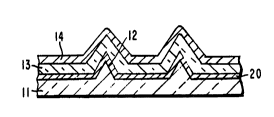
Referring to the drawings, FIGS. 1 and 2 show side
and top views, respectively, of a substrate 11 having field
emitter elements 12 formed on a surface of the substrate.
The substrate 11 and the field emitter elements 12 may be
of polysilicon, for example. The substrate 11 is
fabricated in a conventional manner to provide an array of
emitter elements thereon, with FIG. 2 showing a typical
field emitter array. Typically, the substrate 11 and the
field emitter elements 12 have a metal layer 20 disposed
thereover. This metal layer 20 may be of molybdenum, for
example. The metal layer 20 is typically deposited over
elements 12 and substrate 11 to a thickness of from about
250A to about 2000A, for example. It should be understood,
however, that the metal layer 20 may be eliminated in some
applications.
Referring to FIG. 3, a layer of oxide 13 is deposited
over the surface of the substrate 11 and the field emitter
elements 12 (or the metal layer 20 if it is employed). The
oxide layer 13 is typically formed using a chemical vapor
deposition process. The oxide layer 13 is deposited to a
thickness of from about 5000A to about 15000A, for
example. A gate metal layer 14, comprising a layer of
chromium and a layer of gold, for example, is then
deposited over the layer of oxide 13. The chromium layer
may have a thickness of from about 300A to about loooA,
while the gold layer may have a thickness of from about
2000A to about 5000A, for example.
With reference to FIG. 4, a layer of photoresist 15
is then deposited over the gate motal layer 14. The layer
of photoresist 15 is typically deposited using a
conventional spin-on procodure employing Hoechst AZ 1370
photorosist spun on at 4000 RPM for about 20 seconds, for
oxample.
,
:
: .
203~81
1 The structure of FIG. 4 is then processed to cause
portions of the layer of photoresist 15 above respective
field emitter elements 12 to be remo~ed, as shown in FIG.
5, and thereby expose respective portions of the gate metal
layer 14 above respective tip regions of the field emitter
elements 12. This may be accomplished by plasma etching
the layer of photoresist 15 in an oxygen environment. The
plasma etching operation may be carried out in a plasma
discharge stripping and etching system Model No. PDS/PDE-
301 manufactured by LFE Corporation, Waltham,
Massachusetts, for example. As a specific example for
illustrative purposes, in performing such a plasma etching
process on a field emitter array structure having the
aforementioned specific parameters, the aforementioned
plasma discharge system may be initially evacuated to a
pressure of about 0.1 torr, after which a regulated flow of
oxygen gas may be passed through the system at a flow rate
of about 240 cc per minute and at a pressure of about 3
torr before commencement of the plasma discharge. A plasma
di~charge is then established in the system for a
predetermined time to achieve the desired photoresist
removal. As a specific example for illustrative purposes,
when a single 2-inch wafer having a field emitter array
~tructure formed thereon with the aforementioned parameter
values is processed in the aforementioned system at a
plasma discharge power setting of about 250 watts, a plasma
etchlng duration of about 2 minutes has achieved the
de~ired photoresist removal.
As a re6ult of the plasma etching step,
preci~ely-aligned openings 16 are formed directly over
re~pective field emitter elements 12 of the array. The
size of the openings 16 may be controlled by appropriately
controlling process parameters, including time and power
setting of the pla~m~ discharge apparatus and/or the
initial thickne~s o~ the layer of photoresist 15.
.,., .. , ,,.. , ; ", ~ .. .. ,. .;, --
.
~..... 7 :
':'.: :. , ':
,:: - ' ', ' ~' " ,:~'
:' ' ; . '
:' ' ' :-' ' '' '
:: ' ' . . .:
203~81
1 With reference to FIG. 6, the field emitter elements
12 that have been exposed via openings 16 in the preceding
- step are then etched by means of a conventional etching
procedure, for example, using the layer of photoresist 15
as a mask. For example, a mixture of water and potassium
iodide may be employed for a time duration of from about 1
minute to about 5 minutes to etch the gold, for example,
and potassium permanganate for about 7 seconds, and oxalic
for about 7 seconds may be employed to etch the chromium,
for example.
Referring to FIGS. 7 and 8, the layer of photoresist
15 is then removed, and the layer of oxide 13 is etched
using a conventional etching procedure using buffered
hydrogen fluoride, for example, to expose the field emitter
elements 12. This results in a self-aligned cathode
structure as shown in FIG. 8.
With reference to FIGS. 9 and lO, additional
processing steps are illustrated that enable fabrication of
a self-aligned anode structure above the field emission
cathode structure fabricated pursuant to the process of
FIGS. 1-8. ~o fabricate the anode structure after the
photoresist layer 15 is removed as shown in FIG. 7, a
second layer of oxide 17 is deposited on top of the gate
metal layer 14, after which an additional layer of metal
18, which may serve as an anode metal layer in the
resultant device, is deposited over the second layer of
oxide 17.
Next, the Qtructure of FIG. 9 is processed in a
manner described above with respect to FIGS. 4-8. In
particular, a layer Or photoresist i9 applied to the top
~urrace Or the anode metal layer 18 and is then plasma
etched to remove portions of the layer of photoresist above
the elements 12. The anode metal layer 18 is then etched
using the layer of photore~i~t as a ma~k. The layer o~
3s photoresist i5 then removed, and the first and second oxide
layers 13,17 are etched to expose the field emitter
elements 12, resulting in the structure shown in FIG. 10.
203~8~
1 It is to be understood that the above-described
embodiments are merely illustrative of some of the many
specific embodiments utilizing the principles of the
present invention. Clearly, numerous and other
arrangements can be readily devised by those skilled in the
art without depart.ing from the 6cope of the invention. For
example, metal may be used instead of polysilicon to form
the substrate and the emitter element6. Also, dry etching
of the oxide and metal layers may be employed where
anisotropic etching is critical. In addition, the gate
metal layer may be comprised of metal alloys other than
chromium and gold, such as by molybdenum, for example.
..
: ,
.
: . . ..
'