Note: Descriptions are shown in the official language in which they were submitted.
- NE-298
2034634
,
TITLE OF THE INVENTION
2 "Spread Packet Communication System"
3 BACKGROUND OF THE INVENTION
4 The present invention relates generally to satellite packet
s communications systems, and more specifically to a spread packet
6 communication system.
7 The slotted and unslotted ALOHA packet communication systems
8 are well known. In these systems, very small aperture terminal (VSAT)
9 stations randomly transmit their data packets in burst form via a satellitetransponder to a central station. A modified version of the ALOHA
1 1 system is the spread ALOHA network which was proposed in 1986 by
12 Norman Abramson and is described in "Spread ALOHA for VSAT
13 Networks", Norman Abramson, Technical Report B86-4b, University of
14 Hawaii, June, 1986 (rev. 1/87). According to this technique, packet data
from each VSAT station are distributed or "spread" on the time domain
16 using a coded sequence of pseudorandom numbers in order to reduce
17 the probability of burst collisions and to reduce per-bit transmission
18 power. Two spread modes are known. One is the bit spread ALOHA in
19 which each data bit is spread into a plurality of pseudorandom code
bits, and the other is the chip spread ALOHA in which each
21 pseudorandom code bit (or chip) is spread with the data bits of a
22 packet. No implementations of the proposed spread ALOHA system
23 have yet been made due to anticipated hardware complexities of
24 central station's demodulator system which must be synchronized with
high-speed chip-rate clock pulses to detect correlations between
26 received data bits and a pseudorandom number (PN) sequence.
27 SU M MARY OF THE I NVENTION
2 8 It is therefore an object of the present invention to provide a spread
2034~3D,
71024-147
packet communications system which simplifies the hardware of its
central station equipment.
According to a broader aspect, there is provided a
satellite packet communication system comprising a central station
which generates chip-rate clock pulses and transmits a series of
data on timeslots of a frame to a satellite transponder, and a
plurality of terminal stations. Each terminal station receives
the frame from the transponder and recovers the chip-rate clock
pulses from the received frame. The terminal station includes a
pseudorandom number (PN) sequence generator synchronized with the
recovered chip-rate clock pulses for generating bits of a PN
sequence with which packetized data bits are pseudorandomly
modulated and transmitted in burst form to the transponder. The
central station includes a correlator which is synchronized with
the central station's chip-rate clock pulses to detect
correlations between the pseudorandomly modulated data bits and a
sequence of pseudorandom numbers corresponding to the PN sequence
bits of the terminal stations.
The hardware simplification for bit spread packets is
obtained by recovering the chip-rate clock pulses from the data
rate of a received frame signal in each terminal station.
Specifically, the central station of a bit spread packet
communication system generates chip-rate clock pulses, derives
data-rate clock pulses from the chip-rate clock pulses, and
transmits a series of data in synchronism with the data-rate clock
pulses on timeslots of a frame to a satellite transponder. Each
terminal station includes a data-rate clock recovery circuit which
2034634
71024-147
recovers data-rate clock pulses from the frame signal received
from the transponder and a chip-rate clock recovery circuit for
recovering chip-rate clock pulses from the recovered data-rate
clock pulses for synchronizing the pseudorandom number (PN)
sequence generator.
In order to compensate for different round-trip
propagation delay times among the terminal stations, the central
station receives its own frame signal from the transponder and
recovers the data-rate clock pulses from the received frame. A
first chip-rate clock recovery circuit recovers chip-rate clock
pulses from the recovered data-rate clock pulses and a second
chip-rate clock recovery circuit is provided for recovering chip-
rate clock pulses from an output signal of the correlator. A
phase detector is connected to the first and second chip-rate
clock recovery circuits for detecting a phase difference between
their output signals and a signal indicating the detected phase
difference is transmitted on a timeslot to the transponder. Each
terminal station receives the phase-difference signal on an
assigned timeslot and controls the phase timing of the chip-rate
clock pulses which are supplied to the PN sequence generator
according to the phase-difference signal.
In order to minimize the interference caused by burst
collisions, each terminal station recirculates the PN sequence
generator by k bits, where k is in the range between 1 and m-1,
where m is the number of bits in the PN sequence. Packetized data
bits from each terminal station are synchronized with the
recovered data-bit clock pulses. The central station's correlator
2034634
71024-147
includes 2xm multipliers which are divided into first and second
groups, the multipliers of each group having m pseudorandom
numbers. The k value of each terminal station differs from the k
value of the other terminal stations.
The hardware simplification for chip spread packets is
obtained by recovering chip-rate clock pulses from the start
timing of a received frame signal at each terminal station.
Specifically, the central station generates chip-rate clock pulses
corresponding to timeslots of a frame and transmitting a series of
data on the timeslots to a satellite transponder. Each terminal
station receives the frame from the transponder, detects the start
timing of the received frame and recovers the chip-rate clock
pulses from the detected frame start timing for synchronizing the
PN sequence generator.
The invention may be summarized, according to a broad
aspect, as a satellite packet communication system comprising: a
central station including means for generating chip-rate clock
pulses and up-converter means for transmitting a series of data on
timeslots of a frame to a satellite transponder, said data being
synchronized with said chip-rate clock pulses; and a plurality of
terminal stations each comprising: (i) down-converter means for
receiving said frame from said transponder; (ii) chip-rate clock
recovery means for recovering the chip-rate clock pulses from the
received frame; (iii) a pseudorandom number (PN) sequence
generator synchronized with said recovered chip-rate clock pulses
for generating bits of a PN sequence; (iv) pseudorandom modulator
means connected to said PN sequence generator for pseudorandomly
2034634
71024-147
modulating packetized data bits with said PN sequence bits;
(v) digital modulator means connected to said pseudorandom
modulator for modulating the pseudorandomly modulated packetized
data bits upon a burst carrier to produce a modulated carrier
burst; and (vi) an up-converter for transmitting the modulated
carrier burst to said transponder, said central station further
comprising a down-converter for receiving the carrier burst of
each terminal station via said transponder, correlator means
connected to said down-converter and synchronized with the central
station's chip-rate clock pulses for detecting correlations
between pseudorandomly modulated data bits of the received carrier
burst and a sequence of pseudorandom numbers corresponding to said
PN sequence of the terminal stations, and digital demodulator
means connected to said correlator means for demodulating the
detected correlations to generate a replica of packetized data
bits of each of said terminal stations.
BRIEF DESCRIPTION OF THE DRAWINGS
The present invention will be described in further
detail with reference to the accompanying drawings, in which:
Fig. 1 is a block diagram of a bit spread ALOHA
satellite communication system according to a first embodiment of
the present invention;
Fig. 2 is a waveform diagram associated with Fig. 1;
Fig. 3 is a block diagram of a bit spread ALOHA
satellite communication system according to a second embodiment of
the present invention;
Fig. 4 is a block diagram of a bit spread ALOHA
-
2034634 7l024-l47
satellite communication system according to a third embodiment of
the present invention;
Figs. 5A and 5B are illustrations of colliding data bit
streams associated with Fig. 4;
Fig. 6 is a block diagram of a chip spread ALOHA
satellite communication system of the present invention; and
Fig. 7 is a waveform diagram associated with Fig. 6.
DETAILED DESCRIPTION
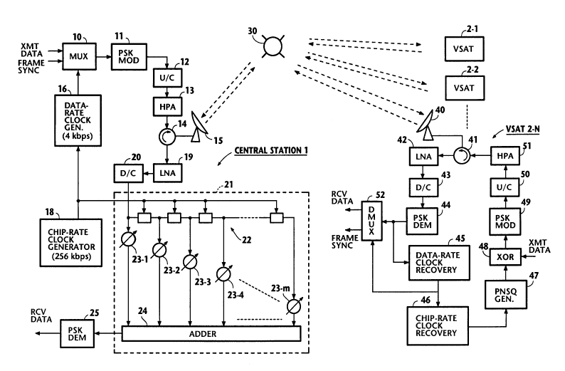
Referring now to Fig. 1, there is shown a spread ALOHA
satellite communication system according to one embodiment of the
present invention. The system comprises a central station 1 and a
plurality of VSAT (very small aperture terminal) stations 2-1
through 2-N interconnected with the central station via a
satellite transponder 30.
Central station 1 comprises a chip-rate clock generator
18 which supplies 256-kbps chip-rate clock pulses to a data-rate
clock generator 16. Data-rate clock generator 16 divides the
frequency of the chip-rate clock pulses by a factor 64 and
supplies a 4-kbps data-rate clock pulse to a multiplexer 10 in
which 4-kbps transmit data is multiplexed with frame sync codes.
The multiplexed signal is applied to an M-ary PSK (phase-shift
keyed) modulator 11 where it is digitally modulated upon a
carrier. The output of PSK modulator 11 is coupled to an up-
converter 12 in which the PSK-modulated signal is translated to a
satellite's up-link frequency and passed through a high-power
amplifier 13 and a diplexer 14 to the central station antenna 15
for transmission to the satellite transponder 30.
5a
2034634
71024-147
A signal from each VSAT station is transmitted in burst
(packet) form to transponder 30 and received at the central
station by antenna 15 and applied through diplexer 14 and a low-
noise amplifier 19 to a down-converter 20 where it is translated
to a baseband frequency and applied to a correlator 21.
Correlator 21 includes a tapped delay line 22 which is clocked by
the chip-rate clock generator 18 to successively shift the PSK-
modulated bit stream at the chip rate of 256 kbps. Successive
taps of the delay line 22 are coupled respectively to multipliers
23-1 through 23-m which are respectively set to different values
(+1 and -1) corresponding to the bits of a pseudorandom sequence
with which the original packet data bits of each VSAT station have
been modulo-2 summed, or "spread". The outputs of multipliers 23
are summed by an adder 24 of coupling to a PSK demodulator 25.
5b
NE-298
2034634
- 6 -
The frame signal from central station 1 is retransmitted from
2 transponder 30 in a broadcast mode to all VSATs. Each VSAT receives
3 the broadcast signal by antenna 40 and applies it through a diplexer 41
4 and a low-noise amplifier 42 to a down-converter 43 in which it is
s translated to a baseband frequency. The output of down-converter 43
6 is coupled to a PSK demodulator 44 to which a data-rate clock recovery
7 circuit 45 is coupled to recover the data-rate clock pulse. The recovered
8 data-rate clock is applied to a demultiplexer 52 to demultiplex the
g output of PSK demodulator into frame sync and data inserted on the
10 timeslot assigned to the VSAT station. The output of data-rate clock
11 recovery circuit 4S is applied to a chip-rate clock recovery circuit 46
12 which recovers the original 256-kbps chip-rate clock by multiplying the
13 recovered data-rate clock frequency by a factor of 64.
14 The output of chip-rate clock recovery circuit 46 is applied to a
15 pseudorandom number (PN) sequence generator 47 to drive it at the
16 chip-rate to produce a m-bit pseudorandom number sequence as
17 specified for all VSATs of the satellite communication system. The
18 output of PN sequence generator 47 is applied to one input of an
19 exclusive-OR gate 48. Transmit packet data is applied to the other input
20 of exclusive-OR gate 48 in which each data bit is modulo-2 summed
21 with the PN sequence.
22 As illustrated schematically in Fig. 2, a portion of the packet data
23 which is represented by a series of "10110" bits is modulo-2 summed
24 with a PN sequence which is, for purposes of simplicity, shown as a
2 5 sequence of "11010010" at a chip-clock rate eight times higher than the
2 6 data bit rate. As a result of the modulo-2 summation, each data bit U1 "
27 of a packet is converted to a sequence of reversals of the 8-bit PN
28 sequence and each data bit "0" is converted to a bit sequence having
2034634
71024-147
the same bit pattern as the 8-bit PN sequence.
The spread bit stream is applied to a PSK modulator 49
where it is used to modulate a burst carrier, the modulated burst
carrier being translated to an up-link frequency by an up-
converter 50. After high-power amplification by amplifier 51, the
up-link signal of the VSAT station is applied through diplexer 41
to antenna 40 for transmission to central station 1 via
transponder 30.
At the central station, the PSK-modulated carrier burst
appears at the down-converter 20 and is entered into correlator 21
in which it is shifted at the chip-rate along the tapped delay
line 22, successively multiplied by multipliers 23-1 through 23-m
with the aforesaid pseudorandom values and the outputs of
multipliers 23 are summed altogether by adder 24. Adder 24
produces a positive peak value corresponding to an original
binary-1 data bit or a negative peak value corresponding to an
original binary-0 data bit either when there is a match between
the m-bit pattern of the bit-spread PSK-modulated signal and the
bit pattern of the multipliers 23. Such peak values periodically
occur at the data rate of 4 kbps and are demodulated into the
original packet data by PSK demodulator 25.
Since the chip-rate clock of each VSAT is synchronized
with the 256-kbps reference clock of the central station, the bit-
spread packet data from all VSAT stations are synchronized with
that reference clock. Because of this synchronization, correlator
21 is able to detect the original data bit stream of each packet
synchronously with the common chip-rate clock, thus eliminating
2034634
71024-147
the need for a high-speed chip-rate clock generator and complex
hardware which would otherwise be required for quickly
establishing synchronism with each incoming burst.
Since VSAT stations are located in different places,
their round-
7a
- NE-298
-8- 2034634
trip propagation delays differ from each other to such a degree that a
2 phase difference of less than one chip-clock interval occurs among the
3 packets arriving at the central station.
4 The embodiment of Fig. 3 eliminates the phase difference problem.
s The central station is provided with a polling circuit 66 which
6 periodically sends a polling signal via transponder 30 to each VSAT
7 station to elicit a response therefrom. A PSK demodulator 60 is
8 connected to the output of down-converter 20 to receive and
9 demodulate the central station's polling signal returning from
transponder 30 and supplies it to a clock recovery circuit 61 where the
11 data-rate clock component of the returning signal is detected and fed
12 into a chip-rate clock recovery circuit 62. The latter recovers the chip-
13 rate clock timing and applies it to a phase detector 63 as a reference
14 phase. Another chip-rate clock recovery circuit 64 is connected to the
output of PSK demodulator 25 to recover the chip-rate clock timing from
16 a response signal sent from the polled VSAT station. The output of the
17 chip-rate clock recovery circuit 64 is applied to phase detector 63 for
18 comparison with the reference phase. Phase detector 63 generates a
19 phase difference signal which corresponds to the deviation of the
round-trip propagation delay of that given VSAT from that of the central
21 station. A coded signal representing the detected phase difference is
22 generated by a coder 6S. By receiving a signal from polling circuit 66
23 identifying the polled VSAT, coder 65 supplies the coded phase-
24 difference signal to multiplexer 10 so that it is transmitted on a timeslot assigned to the polled station.
26 Each VSAT station is provided with a polling transceiver 67 and a
27 decoder 68 both connected to demultiplexer 52. The polling signal
28 from the central station is fed into polling transceiver 67. On receiving it,
- NE-298
-9- 2034634
transceiver 67 applies a response signal to exclusive-OR gate 48 to cause
2 it to be spread with the PN sequence for transmission to the central
3 station. On the other hand, the coded phase-difference signal from the
4 central station is demultiplexed and supplied to the decoder 68 of the
5 polled VSAT station. A phase shifter 69 is connected between the
6 output of chip-rate clock recovery circuit 46 and PN sequence generator
7 47. Phase shifter 69 receives the output of decoder 68 to introduce a
8 delay to the chip-rate clock pulses by an amount corresponding to the
9 round-trip propagation delay time difference of the own VSAT station
10 with respect to the reference timing. Therefore, the chip-rate clock
11 pulses of all VSAT stations are individually controlled at periodic intervals12 to compensate for their chip-rate phase timing differences.
13 Fig. 4 shows a third embodiment of this invention. Before
14 describing this embodiment, it is appropriate to describe the tolerant
15 nature of the spread ALOHA system to interference when two packets
16 are simultaneously transmitted from VSAT stations of different systems.
17 Assume that VSAT station 72-1 sends a sequence of data bits Aj (where
1 8 i = 1, 2, 3 ...) and VSAT station 73-1 transmits data bits Bj. The data bit
19 of each VSAT station is spread with a pseudorandom bit sequence X1,
X2, .... Xm so that their transmitted sequences are represented by AjX1,
21 AjX2, .. AjXm and BjX1, BjX2, .. BjXm. It is further assumed that
22 there is a collision between these spread bit sequences such that the
23 sequence AjX1, AjX2, .. AjXm overlaps (m - k) bits of the sequence
24 BjX1, BjX2, .. BjXm and k bits of the next sequence Bj+lX1, Bj+1X2,
2 5 Bj+lXm as shown in Fig. 5A (where k is in the range between 1 and m -
2 6 1). Since the correlator of central station 71-1 is synchronized with the
27 bit sequence AjX1, AjX2, ..... AjXm, the following correlation output is
28 generated by the correlator:
- NE-298
-l- 2034634
m m-k m
{ i=l j i+k) i+i ~k (Bj+lXi-m+k)Xi) (1)
2 The first term of Equation (1 ) corresponds to the component that is
3 wanted and the second term corresponds to the component generated
4 as a result of the interference. If the autocorrelation coefficient of the PN
5 sequence X at delay time "i" is represented by Cj, the latter is at a peak
6 value if i = 0 and is much smaller than the peak value if i ~ 0. For
7 example, if the X sequence is a maximum length sequence, Cj = m for
8 i=0 and ICjl = 1 for i ~ 0. By rearranging Equation (1 ) using the notation
9 Cj, the following Equations yield if Bj = Bj+1:
y(t) = Ai Co + Bj Ck (2)
1 1 and if Bj ~ Bj+1:
rm-k m
1 2 y(t) = Ai Co+ Bj ~ ~ Xi+k Xi - ~, Xi_m+kXi ~ (3)
~ i=l i=m-k+l J
13 The second term of Equation (2) is significantly smaller than the first
14 term of Equation (1), and therefore the data bit sequence Aj can be
15 correctly received. However, the second term of Equation (3) cannot be
1 6 minimized.
17 In order to minimize the second term of Equation (3), each VSAT
1~ station is provided with a pattern shifter 70 which supplies a control
19 signal to PS sequence generator 47 for periodically and/or randomly
20 recirculating its m-bit PN sequence by k bits. For example, if one VSAT
21 station has the PN sequence of Fig. 2 (i.e.,"11010010"), the PN
22 sequence of another VSAT station is recirculated as as sequence
23 "10100101". A shift register 72 is connected to the data input of
24 exclusive-OR gate 48 to store transmit packet data and forward it to
25 exclusive-OR 48 in response to the output of data-rate clock recovery
2 6 circuit 45. In this way, the transmit data bit timing of each VSAT station
~- NE-298
11- 2034634
is synchronized with the other VSAT stations.
2 The central station is provided with a correlator 73 having a tapped
3 delay line 74 with twice as many delay units as those of the tapped
4 delay line of the previous embodiments. Likewise, twice as many
multipliers 751 through 752m are provided as those of correlator 21 of
6 the previous embodiments. Multipliers 751 through 752m are equally
7 divided into a first group of multipliers 751 to 75m and a second group
8 of multipliers 75m+1 to 752m and the multipliers of each group are set
g with the same PN sequence Xl, X2, .. Xm.
Assume that there is a collision between the bit sequence AjXl,
11 AjX2, .. .AjXm from VSAT 2-1 and a bit sequence BjXl+k, BjX2+k,
12 BjXm, .. BjXk from VSAT 2-2. Since the bit sequence Bj is displaced by k
13 bits with respect to the bit sequence Aj, and the data bit timing of both
14 packets is aligned with each other as shown in Fig. 5B, bit sequence A
15 matches its PN sequence which is set to multipliers 751 to 75m.
6 Correlator 73 produces an output signal z(t) from adder 76 for the bit
17 sequence Aj which is given as follows:
m rm-k m
18 z(t)= ~(AiXi)Xi+~ ~(BjXi+k)Xi+i ~;k l(Bj+lXi-m+k)XiJ
19 =AiCo+Bjck
Since z(t) is equal to y(t) of Equation (2), the interference caused by
21 colliding packets can be held to a minimum and the bit sequence Aj can
22 be correctly received. Following the detection of bit sequence Aj, bit
23 sequence Bj matches its PN sequence which is set to multipliers 751+k to
2 4 75m+k-
While mention has been made of embodiments in which each data
2 6 bit is spread with an m-bit PN sequence whose clock rate is higher than
27 the data clock rate, the present invention could equally be as well
N E-298
-12- 2034634
employed for applications in which the binary levels of the whole data
2 bits of each packet are randomly reversed or not depending on the
3 binary level of each bit of a spreading PN bit sequence using a chip-
4 clock rate lower than the data-rate clock. As illustrated in Fig. 6, the
5 central station is provided with a time base 80 to supply reference clock
6 pulses to a chip-rate clock generator 81 as well as to data-rate clock
7 generator 16. Chip-rate clock generator 81 converts the frequency of
8 the reference clock to a lower frequency corresponding to the slot
9 timing of the frame signal and causes correlator 21 to be synchronized
10 with the time-slot frequency.
11 On the other hand, each VSAT station has a chip-rate clock
12 recovery circuit 82 which receives frame sync from demultiplexer 52 to
13 recover the original chip-rate clock for driving a PN sequence generator
14 83 at the chip-rate, i.e., the time-slot frequency. The PN sequence is a
15 maximum length sequence with a period covering a plurality of time
16 slots. Fig. 7 shows only a portion of the PN sequence. This PN
17 sequence is modulo-2 summed by exclusive-OR gate 48 with transmit
18 data bits to produce packet-spread data bits as shown in Fig. 7.
19 The foregoing description shows only preferred embodiments of
20 the present invention. Various modifications are apparent to those
21 skilled in the art without departing from the scope of the present
22 invention which is only limited by the appended claims. Therefore, the
23 embodiments shown and described are only illustrative, not restrictive.