Note: Descriptions are shown in the official language in which they were submitted.
~0~4638
Title of the Invention
A Data Conversion System
Technical Field of the Invention
This invention pertains to a data conversion system
for a pattern recognition device, and more particularly to a
data conversion system for line-narrowing a pattern, for ex-
tracting its features. A data conversion system used accord-
ing to the invention is in a systolic array for fine-line
character stroke information by a systolic array structure.
Background of the Invention
A CPU conventionally performs a line-narrowing pro-
cess in one-dot units, which has the disadvantage of taking
relatively long time. A system for reading inputted data with
high dot number per unit area with a high degree of accuracy
takes a particularly long time.
If there is a limitation that only lines under a
certain width are read, a predetermined number of line-
narrowing processings need to be performed. However, if theinputted data are recognized in character units, a disadvan-
tage arises that unnecessary line-narrowing (once a line-
narrowing is achieved, no changes are produced by repeating
line-narrowing) still needs to be executed, thus consuming
even more time.
This invention aims at providing a data conversion
system for expediting a pattern recognition first by parallel
~ 28151-24
~^
,, -
2 203463~
processing in a pipeline in a processing unit, second by elim-
inating unnecessary line-narrowing processings, and third by
parallel processings in a pipeline with a systolic array for
line-narrowing.
Description of the Prior Art
As a result of advances in computer technology,
reading devices for receiving image data, extracting charac-
ters from received image data and recognizing respective char-
acters in sentences of the read documents are put into prac-
tical uses. These reading devices divide dot data read, by an
image scanner or similar device into predetermined areas, and
compare the character within each divided area with pre-
registered characters, and outputs the most similar character
as the result.
These predetermined data are generally stored in a
dictionary memory which stores featuring data of the respec-
tively defined characters. When a character to be recognized
is inputted, the inputted character is similarly featured, so
that the distance, i.e. the difference, from the predetermined
featuring data stored in the dictionary memory is obtained.
The character with the least distance is outputted as the
recognition result.
In a recognition other than the pre-treatment, too,
all the processing is performed in one-dot units. For in-
stance, a character in a divided area is extracted as a recog-
nized character, a 3*3 dot window is provided for obtaining
28151-24
2034638
the featuring data of the character from the 3*3 dot data. As
in the pre-treatment, the 3*3 dot window is read in one-dot
units by the CPU. When a memory can be accessed in 8-bit
units, the neighbouring 3 bits of data (e.g. 8 dots in a row)
are read out in a single access, and then data in the next row
are accessed, so that the newly read dots in the 3*3 dot
window are sequentially processed.
When featuring data in the dot window are all ob-
tained, the dictionary memory is sequentially accessed in
character units by the featuring data, so that the distance
from the featuring data is obtained. By comparing the dis-
tances from the featuring data for the respective characters,
the character of the nearest distance (with the least differ-
ence) is outputted as the recognition result, or alterna-
tively, the top-ranked three (3) or five (5) characters are
outputted as candidate characters.
There are various methods for obtaining the-featur-
ing data. One is to recognize an inputted character by ex-
tracting its feature from the vector direction of a single
narrowed line of one-dot width. This method compares the
vector direction, i.e. the feature vector, of the inputted
character with that of the character stored beforehand by
equating the sizes of the inputted data through an advance
normalization.
This method for line-narrowing requires a line-
narrowing circuit. However, conventionally the line-narrowing
circuit judges whether or not the dots around the center dot
28151-24
203~638
of e.g. 3*3 dots of the extracted character area are black or
white, and determines whether or not to make the center dot
white.
That is, for line-narrowing of one-dot width, eight
(8) dots around the center dots are read dot by dot and their
states (of white or black) determine the state of the center
dot.
For this judgment, a plurality of dots around (in a
total of eight directions from) the center dot need to be read
dot by dot, thus a problem exists that a relatively long time
is required to call up the plurality of dots to ~udge one dot.
To reiterate, since a long time is required for
line-narrowing, recognition processing in character
recognition take a long time.
Summary of the Invention
The first principle enables parallel pipeline
processing to narrow lines sequentially at a high speed,
line-narrowing in a pattern recognition device, as well as a
pattern recognition is expedited.
The second principle uses a conversion window, e.g.
of 3*3 dots, conversion data such as stroking data corres-
ponding to the center cell are obtained faster, each time
image data are inputted in dot-row units or in dot-column
units.
The third principle sequentially supplies character
data in dot-column units in parallel, so that the center dot
28151-24
-- 203463~
of a mask comprising e.g. 3*3+2 dots is judged to be white or
black according to the surrounding dots, it saves unnecessary
conversion processing in line-narrowing, by converting a
series of character data, e.g. in a 64*64 dot unit, thereby
data conversion such as line-narrowing is expedited.
In accordance with a first aspect of the invention,
there is provided a data conversion system utilizing a cell
comprising shift register means for receiving a first plural-
ity of data and a second plurality of data, said shift reg-
ister means also for sequentially shifting the first pluralityand second plurality of data, said shift register means having
a first shift register which shifts the first plurality of
data and a second shift register which shifts the second
plurality of data; a memory, coupled to said shift registers,
said memory containing predetermined values which are out-
putted when data in said shift register means are supplied as
an address and used to determine a value of a center dot of an
area, and an instruction signal which outputted is for deter-
mining the value of the center dot according to dot data
outside of the certain area when data in the certain area are
not in a pattern which is used to determine the value of the
center dot of the area; and an operation means for selecting
and outputting said predetermined values from said memory when
no instruction signal is supplied from said memory and for
outputting the value of the center dot by determining it from
data outside the certain area per the instruction signal.
28151-24
.~.,~ .
:..,J~
203463~
In accordance with a second aspect of the invention,
there is provided a data conversion system for outputting data
in n*3 pieces of windows respectively corresponding to said
plurality of data by providing a plurality of cells each com-
prising: a first shift register comprising a register of n
stages for supplying inputted data to the neighbouring cells
on both sides and for sequentially shifting said inputted
data; a second shift register comprising a register of n
stages supplied with data from a neighbouring cell for sequen-
tially shifting the supplied data; and a third shift registercomprising a register of n stages supplied with data from a
neighbouring cell for sequentially shifting the supplied data;
and a memory for memorizing conversion data corresponding to
said n*3 pieces of data by supplying n*3 pieces of data
shifted by said first, second and third shift registers to
their address terminals.
In accordance with a further aspect of the inven-
tion, there is provided a data conversion system utilizing: a
shift register comprising a plurality of stages for sequen-
tially shifting N bits of data supplied for the next register;a memory, supplied with data memorized in said shift register
as addresses, for outputting data stored in advance; a FIFO
for memorizing data outputted from said memory and supplying
said memorized data to a first stage of said shift register
comprising a plurality of stages; and a detection circuit for
detecting a change in data shifted in said plurality of shift
registers and FIFO during a data circulation in a loop by
comparing a part of data supplied to the addresses of said
memory with an output from said memory.
28151-24
~,
~ 2034638
6a
In accordance with a further aspect there is also
provided a data conversion system for converting an input
image data to a line-narrowed image data in a pattern recog-
nition process, comprising: a plurality of cells connected on
parallel for receiving a plurality of dot data representing
the input image data, each cell including: shift register
means supplied with a part of said plurality of dot data which
includes a dot data not input to a neighbouring cell, for se-
quentially shifting said part of the dot data; and memory
means supplied with dot data in a certain area of the shift
register means as an address for stored data to output a pre-
determined value corresponding to a pattern of the dot data in
the certain area.
In accordance with a further aspect there is also
provided a data conversion system utilizing a cell comprising:
shift register means for receiving a first plurality of data
and a second plurality of data, said shift register means also
for sequentially shifting the first plurality and second plur-
ality of data, said shift register means having a first shift
register which shifts the first plurality of data and a second
shift register which shifts the second plurality of data; and
a memory coupled to said shift registers, said memory contain-
ing predetermined values which are outputted when data in said
shift register means are supplied as an address and used to
determine a value of a center dot of an area.
28151-24
B~
6b 2034638
Brief Description of the Drawings
Figure lA is a block diagram illustrating a first
principle of this invention;
Figure lB is a block diagram illustrating a second
principle of this invention;
Figure lC is a block diagram illustrating a third
principle of this invention;
Figure 2A shows a system configuration of a
character-recognizing device using an image data normalization
circuit of this invention;
Figure 2B shows a configuration of an association
dictionary;
Figure 3 shows in detail the circuit configurations
of a row-histogram module and a column-histogram module using
the first principle of this invention;
Figure 4 explains the operations and the circuit
configurations of the row-histogram module and the
column-histogram module using the first principle of this
invention, described in Figure 3 further in detail;
Figure 5 shows the detailed circuit
28151-24
-
7 20346~B
configurations of the row-histogram module and the
column-histogram module using the first principle of
this invention;
Figure 6 shows schematically the configurations
of the row-histogram module and the column-histogram
module using the first principle of this invention;
Figure 7 explains the operations of the row-
histogram module and the column-histogram module using
the first principle of this invention;
Figure 8 shows the operations of the horizontal
histogram calculation of the row-histogram module and
the column-histogram module using the first principle
of this invention;
Figure 9 shows the operations of the vertical
histogram calculation of the row-histogram module and
the column-histogram module using the first principle
of this invention;
Figure 10 is a flowchart of the character
recognition method in a normalization module using the
first principle of this invention;
Figures 11A and 11B show an example for a non-
linear normalization in the normalization module using
the first principle of this invention;
Figure 12 illustrates creations of conversion
functions in the normalization module using the first
2~346~8
pr inc ip le of thi s i nvent i on;
Figure 1 3 shows a loop program f or a
normalization by the normalization module using the
first principle in this invention;
Figure 14 shows an example of converted data at
various stages of a normalization by the normalization
module using the first principle of this invention;
Figure 15 shows a schematic view of an array in
the normalization module using the first principle of
1 this invention;
Figure 16 shows a configuration of a cell in the
normalization module using the first principle of this
invent ion;
Figure 17 shows an input sequence of shi f ted data
in the normalization module using the first principle
of this invention;
Figure 1 8 shows various examples of
normalizations of the same character in the
normalization module using the first principle of this
2 i nvent i on;
Figure 19 shows an algorithm for a histogram
calculation in the normalization module using the
first principle of this invention;
Figure 20 shows adjustments of obliquenesses in
the normalization module using the first principle of
9 20~ 1638
this invention;
Figure 21 explains the principle of
magnification by the row-histogram module and the
column-histogram module using the second principle of
5 this invention, which utilizes a systolic array;
Figure 22 shows the configurations of the row-
histogram module and the column-histogram module using
the second principle of this invention, which utilizes
a systolic array;
Figure 23 shows exemplary histograms in the
vertical and horizontal directions of the row-
histogram module and the column-histogram module using
the second principle of this invention, which utilizes
a systolic array;
Figure 24 shows the histogram generation circuit
network of the row-histogram module and the column-
histogram module using the second principle of this
invention, which utilizes a systolic array;
Figure 25 shows an input sequence of shifted data
20 of the row-histogram module and the column-histogram
module using the second principle of this invention,
which utilizes a systolic array;
Figure 26 shows in detail the configuration of a
linear histogram computing cell of the row-histogram
25 module and the column-histogram module using the
1 o 2 0 3 ~ 6 CJ 8
second principle of this invention, which utilizes a
systolic array;
Figure 27 shows an exemplary horizontal histogram
of the row-histogram module and the column-histogram
module using the second principle of this invention,
which utilizes a systolic array;
Figure 28 shows in detail the configuration of a
non-linear histogram computing cell of the row-
histogram module and the column-histogram module using
the second principle of this invention, which utilizes
a systolic array;
Figure 29 shows the configuration of the
normalization circuit network of the normalization
module using the second principle of this invention,
which utilizes a systolic array;
Figure 30 shows the configuration of normalizing
cells of the normalization module using the second
principle of this invention, which utilizes a systolic
array;
20Figure 31 shows the configuration of the
normalization module using the third principle of this
invention;
Figure 32 shows in more detail the configuration
of the normalizing part in the normalization module
using the third principle of this invention;
11 2034638
Figure 33 illustrates the principle of the
normalization module using the third principle of this
invention;
Figure 34 explains the operations of the
normalization part in the normalization module using
the third principle of this invention;
Figures 35A and 35B explain in detail the
operations of the normalization module using the third
principle of this invention;
Figure 36 shows in detail the system
configuration of the normalization module using the
third principle of this invention;
Figure 37 shows in detail the configuration of
the line-narrowing module using the first principle of
this invention;
Figure 38 illustrates the operation of the
conversion in the line-narrowing module using the
first principle of this invention;
Figure 39 is a flowchart of the operations of a
CPU for controlling the line-narrowing module using
the first principle of this invention;
Figure 40 shows in detail the configuration of
the line-narrowing module using the first principle of
this invention;
Figure 41 illustrates in detail the operations of
-
12 203~638
the line-narrowing module using the first principle of
this invention;
Figure 42 shows the configuration of the non-
conformance detection circuit in the line-narrowing
module using the first principle of this invention;
Figure 43 shows the configuration of the line-
narrowing module using the first principle of this
invention;
Figure 44 shows the configuration of a line-
narrowing array in the line-narrowing module using the
second principle of this invention, which utilizes a
systolic array;
Figure 45 shows in detail the configuration of
line-narrowing cells in the line-narrowing module
using the second principle of this invention, which
utilizes a systolic array;
Figure 46 illustrates the pattern positions of
the registers in the line-narrowing module using the
second principle of this invention, which utilizes a
systolic array;
Figure 47 is an input data diagram in the line-
narrowing module using the second principle of this
invention, which utilizes a systolic array;
Figure 48 illustrates data change in the register
of the input data in the line-narrowing module using
2034638
13
the second principle of this invention, which utilizes
a systolic array;
Figure 49 shows the configuration of the stroking
array in the stroking module in its embodiment of this
invention using an array;
Figure 50 shows the configuration of a stroking
cell in the stroking module in its embodiment of this
invention using an array;
Figure 51 shows a matrix of shift registers in
the stroking module in its embodiment of this
invention using an array;
Figure 52 illustrates the operations in the
stroking module in its embodiment of this invention
using an array;
Figure 53 is a stroking table representing shift
register values and an output in the stroking module
in its embodiment of this invention using an array;
and
Figure 54 is a noise reduction table in the
stroking module in its embodiment of this invention
using an array.
Description of the Preferred Embodiments
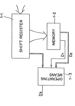
Figure 1A is a block diagram illustrating a first
principle of this invention.
2 0 3 4 6 3 8
14
A part of lmage data ls supplled to a shlft reglster 1-1 whlch
sequentlally shlfts the lnputted data.
Data for a certaln area among the data shlfted at
the shlft reglster 1-1 are supplled to a memory 1-2 as addres-
ses. When the data ls ln a pattern for determlnlng the center
value of the certaln area, the memory 1-2 outputs predeter-
mlned data and a second plurallty of data, sald shlft reglster
means also when the data ls not ln such a pattern, the memory
1-2 stores data for lnstructlng data other than that of the
certaln area ln the shlft reglster 1-1 to determlne the center
value.
An operatlon means 1-3 selects and outputs data Dl
when no lnstructlon slgnal D2 ls supplled from the memory 1-2,
or determlnes and outputs output data D3 accordlng to the data
values of the certaln area lnstructed by the lnstructlon slg-
nal D2, when the lnstructlon slgnal D2 ls supplled.
A systollc array coupled to sald shlft reglsters,
sald memory contalnlng predetermined values whlch are
outputted when data ln sald shlft reglster means are supplled
as an address and used ls conflgured by provldlng a plurallty
of cells wlth each cell comprlslng the shlft reglster 1-1, the
memory 1-2 and the operatlon means 1-3 ln thls lnventlon.
Mutually nelghborlng data among data supplled to each cell
composlng the systollc array are alternatlvely supplIed to the
shlft reglster 1-1. For lnstance, at least three blts of dot
data ln one dot row are supplled to the shlft reglster 1-1.
Data further nelghborlng can addltlonally be supplled.
28151-24
2034638
~ 15
When such dot data are supplied to the input
terminal of the systolic array comprising the cells in one-dot
units, the respective cells sequentially shift the inputted
dot data and supply the corresponding data in the certain area
to the memory 1-2.
The memory 1-2 stores in advance data for outputting
the center dot corresponding to the dot data in advance. The
memory 1-2 stores data for determining the center dot to be
either 0 (for white) or 1 (for black) per the state of eight
(8) dots surrounding the center dot, e.g. in line-narrowing.
Further, where the eight (8) surrounding dots cannot determine
the center dot to be either 0 (for white) or 1 (for black),
the memory 1-2 stores data for instructing dot data other than
the eight (8) dots to determine the center value depending on
whether the dot data of outside cells are 0 (for white) or 1
(for black).
To reiterate, the memory 1-2 outputs a bit which
indicates the center dot value by referencing the surrounding
eight dots or their further outside dots.
When the memory 1-2 outputs the instruction signal
D2 for making the center dot white or black,
28151-24
B
` _ 20~4638
the operation means 1-3 outputs the value of either 0
or 1. Upon receiving a signal instructing it to
reference the outside dots, the operation means 1-3
determines the center dot to be white or black by
taking the data of the outside dots into
consideration.
Since the plurality of cells configure the
systolic array, the data D3 outputted from the
operation means 1-3 are supplied to the corresponding
cell in the next stage, as well as the cells
neighboring the corresponding cell and their
neighboring cells.
When line-narrowing data are stored in the memory
1-2, the above actions enable the cell to output data
after line-narrowing. Since the cells configure the
systolic array, a thick part of a character can be
narrowed sequentially in one-dot units, by providing
the plurality of cells, a fine-line character of only
one-dot width is finally obtained.
Figure 1B is a block diagram illustrating a
second principle of this invention.
The second principle aims at a data conversion in
parallel processings by supplying data to be
recognized to respective cells 2-10, 2-11 and 2-12 in
one-dot units.
17 2 0 3 i 6 ~ 8
A first shift register 2-1 comprising n stages is
for supplying inputted data to the neighboring cells
2-10 and 2-12 on both sides and sequentially shifting
the inputted data.
A second shift register 2-2 comprising n stages
and supplied with data from the neighboring cell 2-10
is for sequentially shifting the supplied data.
A third shift register 2-3 comprising n stages
and supplied with data from the neighboring cell 2-12
opposite to the second shift register 2-2 is for
sequentially shifting the supplied data.
A memory 2-4, comprising e.g. a ROM or a RAM,
receives 3*n bits of data shifted by the shift
registers 2-1, 2-2 and 2-3 at its address terminal and
outputs conversion data corresponding to the 3*n bits
of data.
Data to be converted are supplied to respective
cells 2-10, 2-11 and 2-12 in bit units. The number
of those cells corresponds to the number of dots
inputted simultaneously. The respective cells adds
data inputted to the neighboring cells on both sides.
For instance, the second shift register 2-2 is
supplied with data from the neighboring cell 2-10 and
sequentially shifts the data; and the third shift
register 2-3 is supplied with data from the
2034638
18
neighboring cell 2-12 opposite to the cell 2-10 and
sequentially shifts the data.
The first, second and third shift registers 2-1, 2-2
and 2-3 each comprising e.g. three stages, sequentially shift
their respective inputted data, and store 3*3 dots if the
inputted data are of image data.
The memory 2-4 stores in advance data converted in
correspondence with the 3*n dots of the respective inputted
data. Since the 3*n bits of dot data stored in the first,
second and third shift registers 2-1, 2-2 and 2-3 are supplied
as addresses, the memory 2-4 outputs conversion data
corresponding to the inputted data.
If the converted data stored in the memory 2-4 are
stroking data, second shift data of the first shift register
2-1 represents a predetermined color.
When at least either a first shift datum of the
second shift register 2-1 or a third shift datum of the third
shift register 2-3 represents the predetermined color, the
memory 2-4 outputs a code representing a first direction.
When at least either a third shift datum of the
second shift register 2-2 or a first shift datum of the third
shift register 2-3 represents the predetermined color, the
memory 2-4 outputs a code
28151-24
~03-~638
1 9
representing a second direction.
When at least either a first shift datum or a
third shift datum of the first shift register 2-1
represents the predetermined color, the memory 2-4
outputs a code representing a third direction.
When at least either a second shift datum of the
second shift register 2-2 or a second shift datum of
the third shift register 2-3 represents the
predetermined color, the memory 2-4 outputs a code
representing a fourth direction.
For instance, data in the first row of a
character area are supplied in one-dot units, and 0
and 1 represent white and black, respectively. The
value of the center (the second shift datum of the
first shift register 2-1) of 3*3 dots is 1.
When the second shift datum of the second shift
register 2-2 or the second shift datum of the third
shift register 2-3 is 1, the memory 2-4 outputs a code
representing e.g. a horizontal direction as the fourth
direction.
When the second shift datum of the second shift
register 2-2 or the second shift datum of the third
shift register 2-3 is 1, the memory 2-4 outputs a code
representing e.g. a vertical direction as the third
direction.
203~638
When at least either the third shift datum of the
second shift register 2-2 or the first shift datum of
the third shift register 2-3 is 1, the memory 2-4
outputs a code representing e.g. a 45-degree slash
5 direction as the second direction.
When at least either the first shift datum of the
second shift register 2-1 or the third shift datum of
the third shift register 2-3 is 1, the memory 2-4
outputs a code representing e.g. a 1 35-degree back-
slash direction as the first direction.
Because each time data of 3*3 dots are
sequentially supplied to the memory 2-4 in dot-row
units or in dot-column units they are converted in
one-dot units, the conversion processing is fast.
Figure 1 C is a block diagram illustrating a third
principle of this invention.
Shift registers 3-1 through 3-4 each comprising a
plurality of stages sequentially shift supplied data
of N bits to the next registers. That is, the shift
register 3-1 is supplied with N bits of data. The
shift register 3-2 is supplied with data shifted by
the shift register 3-1. The shift register 3-3 is
supplied with data shifted by the shift register 3-2.
The shift register 3-4 is supplied with data shifted
by the shift register 3-3.
2034638
21
A memory 3-5 receives data stored in the shift
registers 3-1 through 3-4 as its addresses and outputs
previously stored data e.g. conversion data used in
line-narrowing for the N bits of sequentially inputted data.
A FIFO 3-7 memorizes data outputted from the memory
3-5 and supplies the data previously stored in the memory 3-5
to the first stage of the shift register 3-1 comprising the
plurality of stages.
A detection means 3-6 detects by comparing a part of
data supplied to the addresses of the memory 3-5 with the
output from the memory 3-5, whether or not data shifted by the
shift registers 3-1 through 3-4 and the FIFO 3-7 change while
they are circulated in a loop.
The respective shift registers 3-1 through 3-4
comprise a plurality of stages and have inputs and outputs of
N bits, the shift registers 3-1 through 3-4 together form a
shift register of N bits with a plurality of stages. For
example, those shift registers may have data of three (3) bits
with four (4) stages.
Among the data of 3 bits with 4 stages, 3*3+2 bits
of shift data are supplied to the addresses of the memory 3-5
which stores conversion data of the center dot corresponding
to the data supplied to the addresses. This data is stored in
advance e.g. for determining whether the center dot of the
3*3+2 dots is white or black. The output from the memory 3-5
that stores a series of image data converted by the shift
registers 3-1 through 3-4 and the FIFO 3-7 is supplied to the
28151-24
`- 2034638
22
FIFO 3-7. After the series of image data is completely
inputted, data once converted is sequentially outputted from
the FIFO 3-7 again to the shift register 3-1. For instance,
when a line-narrowing circuit is formed, data to the FIFO 3-7
is supplied to the shift register of the next stage.
When this series of actions are performed sequen-
tially, the detection means 3-6 judges whether or not any of
the series of image data supplied to the memory 3-5 change
from the data outputted from the memory 3-5. If the detection
means 3-6 does not detect a non-conformance during the loop
(in which the series of data are circulated for conversions),
since conversions are terminated, the result is outputted.
Since a termination of conversions is detected by a single
non-conversion processing, an unnecessary processing step is
prevented.
The following is a detailed description of this
invention based on the illustration in the drawing.
Figure 2A shows a system configuration of a
character-recognizing device using an image data normalization
circuit of this invention.
Information read by an image scanner or similar
device is stored in an image memory 10 as image data. The
image memory 10 has memory capacity for a page read by the
image scanner. Each dot of the read information is stored as
two-value data of either white or black, i.e. 0 or 1.
Image data, stored in the image memory 10 are
supplied to a noise reduction module 11, where noise generated
28151-24
2034638
23
during reading time is eliminated. The eliminated noise is
irrelevant to the character information. As an example the
noise reduction module 11 treats as white a black dot in a
center of a three-by-three mask pattern in which only the dot
in the center is black and the eight surrounding dots are
white. Although the configuration of this invention provides
the noise reduction module 11 to operate in a character
recognition pre-treatment part 12, it could be set to operate
at some other time, such as, when the read image data are
stored in character units in a normalization module 16 which
will be described later. Alternatively, it could be at a time
of line-narrowing or stroking.
The image data which have undergone a noise
elimination through the noise reduction module 11 are supplied
to a row-histogram module 13, a column-histogram module 14 and
a read control module 15.
The row-histogram module 13 projects the read
information, such as the content of the form read by the image
scanner described earlier, in the row direction and finds the
number of dots in each dot row. That is, it finds the number
of black dots in each dot row (in the horizontal direction).
As in the row-histogram module 13 described earlier,
the column-histogram module 14, projects the read information
in the column direction and finds the number of dots in each
dot unit column.
The row-histogram module 13 sequentially counts the
number of black dots (for each dot row) in data sequentially
28151-24
.~
203463~
24
read in one dot unit in the row direction from the image
memory 10 (similarly to a dot reading by a raster scan) and
supplied through the noise reduction module 11. That is, the
row-histogram module 13 sequentially finds the number of black
dots in each row. The numbers of black dots in respective
rows form a row histogram.
The column-histogram module 14 has counters each
corresponding to a black dot position in a dot row, and
increments the counter corresponding to the black dot position
when a dot in a row is sequentially supplied.
By performing these operations for one page, the
row-histogram module 13 and the column-histogram module 14
respectively obtain a row histogram and a column histogram
each representing the numbers of dots in row positions and
column positions. The result is supplied to the read control
module 15.
The read control module 15 sequentially obtains the
row position and the column position from the row histogram
and the column histogram, respectively. These positions can
be found, for instance, by a cycle of the row histogram or the
column histogram.
The read control module 15 finds the row and column
positions and performs the following additional procedures.
Image data, such as information read by an image scanner, can
have an obliqueness due to a paper position. To cope with
this, the read control module 15 sequentially changes the
28151-24
` 2034638
angle wherewith a histogram is obtained, so that an adjusted
angle is obtained. Then, the image data supplied from the
noise reduction module 11 are reinputted to obtain the final
histogram, so that row data for one cycle period
28151-24
2034638
26
corresponding to the obliqueness are read from the
point whence the row hi stogram ( having a maximum
value ) obtained from the ad justed obliqueness changes
from zero to a positive number (or from a positive
5 number to zero) and stored in a row buffer provided in
the read control module 15.
Further , the read control module 15 again obtains
a column histogram in a row from the row data stored
in the row buffer and cuts out data of one character
10 area to be outputted to a normalization module 16 and
a conversion table creation module 17 from the point
whence the column histogram changes from zero to a
positive number.
The conversion table creation module 17 is for
15 obtaining conversion data for enabling the
normalization module 16 to normalize a character.
The conversion table creation module 17 proj ects the
data of one character area extracted by the read
control module 15 in the column and row directions ,
20 thereby incrementing the respective counters in the
column and row directions by the dot row unit and by
the dot column unit from the column and row with a
black dot, to obtain the final counter value in one
character area.
The normalization module 16 magnifies the size of
2034 638
27
one character area from the size when the character in the
character area is originally extracted, per the final counter
values in the row and column directions of the dots in the
extracted character, to the full sized character which may for
example comprise sixty-four (64) by sixty-four (64) dots.
For example, if the conversion table creation module
17 has forty-eight (48) dots in both the column and row
directions, the normalization module 16 converts a forty-eight
(48) by forty-eight (48) dot character to a sixty-four (64) by
sixty-four (64) dot character, where row and column dot data
of particular positions are repeatedly used as the same data
in magnifying the character.
In case of a contraction, row and column dot data of
particular positions are repeatedly read which are contracted
as the same row and column dot data by "OR" additions.
After the normalization module 16 magnifies a
character to a full sized character, such as of sixty-four
(64) by sixty-four (64) dots, a line-narrowing module 18
narrows the width of the character by using a mask of eleven
(11) dots comprising a center dot and the eight (8) other dots
in the surrounding three (3) by three (3) area as well as the
second left dot and the second up dots from the center dot.
Alternatively a mask used in narrowing could be of nine (9)
dots in the three (3) by three (3) dot area around the center
dot.
The width of a line around a dot of a character can
be narrowed by a control of the earlier described mask whereby
28151-24
`- 2034638
28
a center dot of a predetermined pattern is set to zero. By
repeating the narrowing procedures with masks, lines of a
character are set to a width of one dot.
The narrowed line character, of sixty-four (64) by
sixty-four (64) dots, obtained by the line-narrowing module 18
is supplied to a stroking module 19 for stroking. The strok-
ing module 19 expresses a dot by a total of four kinds of
strokes wherein there is a black dot above or below; right or
left; right above or left below; and left above or right below
an objective dot, such as a center dot. If the objective dot
belongs to plural kinds of strokes among the four (4) kinds
described above, a prioritization, such as the vertical
direction first, the horizontal direction second, etc., for
deciding the kind of stroke the objective dot belongs to.
When the objective dot is white or the center dot value is
zero (0), the stroke is not considered to exist.
Since the stroking module 19 has five (5) cases
wherein a stroke exists in any of four (4) directions, i.e.
vertical, horizontal, slash, and back-slash directions, or
does not exist, the state of each dot is expressed as a three
(3) bit value. The resultant three (3) by sixty-four (64) by
sixty-four (64) bits of information are supplied to a feature
vector module 20.
The feature vector module 20 divides the stroking
information obtained at the earlier described stroking module
19 both horizontally and vertically in eight (8) dot units. A
vector module area of a total of two hundred fifty-six (256)
28151-24
203463~
29
dots, a sixteen (16) by sixteen (16) pattern comprises one of
the divided areas, the area below it, the area to its right,
and the area to its lower right, each having 64 dots. The
feature vector module 20 counts whether or not any of the four
kinds of strokes in the vertical, horizontal, slash and back-
slash directions exists. Although a feature vector is
obtained in a vector module area comprising sixteen (16) by
sixteen (16) dots, since a vector module area is vertically or
horizontally shifted by eight (8) dots, there are seven (7)
feature vector areas in both the row and column directions.
Therefore, each character has a total of forty-nine (49)
vector module areas for feature vectors the first plurality
and second plurality of data, said shift register means having
a first shift register which shifts the first plurality of
data and a second shift register which shifts the second
plurality of data.
When the feature vector module 20 counts the number
of strokes in each of the four directions for the respective
vector module areas described earlier, the feature vector
module 20 weights each dot representing a directional stroke,
such that a center part of a vector module area comprising
sixteen (16) by sixteen (16) dots has a higher weight in
obtaining a feature vector. The weight reduces with distance
from the center. For instance, a dot representing a direc-
tional stroke in the center area comprising four (4) by four
(4) dots has a weight of four (4); a dot representing a di-
rectional stroke in the surrounding harrow area comprising
28151-24
~'
2034638
eight (8) by eight (8) dots, excluding the four (4) by four
(4) dot area at the center, has a weight of three (3); a dot
representing a directional stroke in the outer surrounding
harrow area comprising twelve (12) by twelve (12) dots,
excluding the eight (8) by eight (8) dot area at the center,
has a weight of two (2); and a dot representing a directional
stroke in the outermost harrow area comprising sixteen (16) by
sixteen (16) dots, excluding the twelve (12) by twelve (12)
dot area at the center, has a weight of one (1).
Since the feature vectors set characters to be
recognized to the same size, the same characters (of different
writings) have approximately the same feature vector. That
is, each character has its specific feature vector. However,
since there are very similar characters, an embodiment of this
invention uses standard patterns of feature vectors for class-
ification in each vector module area for a feature vector,
such that a distance is found between a supplied unknown input
and twenty (20) classes of standard patterns in each vector
module area, in order to improve operation processing speed
and recognition rate. That is, the distance is found between
the feature vector of the character to be read in each vector
module area obtained from the feature vector module 20 and the
feature vector of a standard pattern in the vector module
area. Each vector module area is classified into classes 1
through 20, and the order of the classes having class dis-
tances in respective vector modules is found from the smallest
to the fifth-smallest.
28151-24
2034638
31
A distance computing module 21 calculates the dis-
tances by using a class dictionary 23-1 (storing standard
patterns in class units) in a vector dictionary 26. A
candidate dictionary 23-2 is used
28151-24
-
32 2034638
to calculate the distances for respective candidate
characters. (At this time a switch SW selects the
candidate dictionary 23-2.)
An upper rank selection and score assignment
module 22 determines the five (5) top-ranked classes
described earlier and the scores of the corresponding
classes in the respective vector module areas. That
is, the upper rank selection and score assignment
module 22 determines the scores given to the
respective classes of the first to fifth ranks from
the distances obtained by the distance computing
module 21, i.e. the scores of the respective candidate
characters. For instance, five (5) points are given
to the candidate character having the smallest
distance, and decremental points of four (4) through
one (1) are given to respective classes having the
second smallest to the fifth smallest distances.
These procedures are performed for all forty-nine (49)
vector module areas. The processing result of the
upper rank selection and score assignment module 22 is
supplied to a comprehensive rating module 24.
The comprehensive rating module 24 is for
calculating the degree of conformance between an input
objective, i.e. an inputted character, and its
candidate character, and operates in three modes
33 203 1638
comprising an association conformance mode rated by a
score, and a one hundred percent conformance mode and
an individual conformance mode each rated by a
distance.
The association conformance mode is for
calculating the score of a candidate character from
the vector module area corresponding to the candidate
character stored in an association dictionary 23-3 and
a class belonging to the vector module area.
Figure 2B shows the configuration of an
association dictionary.
As shown in Figure 2B, the association dictionary
23-3 stores the identifications for the classes
to which the candidate characters belong in the
respective vector module areas by using the
identifications for the candidate characters in the
respective vector module areas as the addresses.
The association dictionary 23-3 stores only these data
obtained by clustering sets of feature vectors
corresponding to the identifications for the vector
module areas of the respective candidate characters by
their (weighted) distances. The class dictionary
23-1 of the same structure corresponding to the
association dictionary 23-3 is created concurrently in
the distance computing module 21.
34 20~ 1638
When at least two kinds of dictionaries are
stored in one memory, the one to be used is designated
at a dictionary reference starting point. (By
comprehensively rating each of the dictionaries
divided by identifications for the candidate
characters in parallel, they can be referenced at
higher speeds.)
The association dictionary 23-3 is a table
describing the identifications "K" for the classes
wherein a candidate character "a" belongs to a vector
module area "m". By expressing this relation by,
C(m,a)=K
for a candidate character "a"(=1 through c_cand), the
association dictionary 23-3 is obtained as
V(a)=SIGMA(m=1 through c_mask) P(m,C(m,a))
where P(m,K) represents a score, and V(a) represents a
comprehensive rating value for the candidate character
ll ll
a .
The one hundred percent conformance mode and the
individual conformance mode in the comprehensive
rating module 24 are for calculating comprehensive
rating value V(a) for each candidate character "a".
The one hundred percent conformance mode sets a=1
through c_cand; the individual conformance mode sets
J=1 through c_kind and a=b(j); and a distance is
2034638
expressed as d(m,a), in obtaining V(a) which is a (weighted)
distance of the feature vector between the candidate character
"a" and the input object.
V(a)=SIGMA(m=1 through c_mask) d(m,a)
The upper-rank candidate selection module 25 selects
and outputs a plurality of characters, e.g. five (5) top-
ranked characters that become the recognition results of the
read image data.
The operations described earlier are performed in a
pipeline processing. For instance, one page of the image
memory 10 for storing image data are read in a pipeline
processing, divided into rows by the read control module 15
and outputted to the normalization module 16 in a unit of one
character, so that the line-narrowing, stroking, feature
vector making and recognition processing described earlier
are performed.
As described above, the upper-rank candidate
selection module 25 is for selecting the five (5) top-ranked
characters by ranking the candidate characters per the
comprehensive rating value V(a).
The inputs are
(a', V(a)1/2a', a=1 through c_cand revised)
for an association one hundred percent conformance mode; and
28151-24
2034638
36
(j, V(a)l/2j=1 through c_klnd, a=b(j))
The descending/ascending order of the comprehensive
rating value V(a) of the individual conformance mode is se-
quentially from the biggest for character association; and
sequentially from the smallest for others.
Its outputs are identifications for the candidate
characters arrayed in a sorting result of the inputs (or the
inputting order) and their comprehensive rating values V(a).
Figure 3 shows in detail the circuit configuration
of the row-histogram module 13 and the column-histogram module
14 using the first principle of this invention.
The embodiment of this invention shown in Figure 3
provides a two-port DRAM 30 and a DRAM controller 31. The
DRAM controller 31 specifies the addresses supplied to the
two-port DRAM 30 at input and output times. When image data
is supplied to an input terminal (RD) of the two-port DRAM 30
through a FIFO 35, the DRAM controller 31 supplies line data
of a direction of the image data to the same column addresses
as those specified earlier by sequentially changing row
addresses of the two-port DRAM 30. The
28151-24
B
2n3~638
37
DRAM controller 31 is connected to an address bus and
a data bus of a CPU 32. The CPU 32 controls the
DRAM controller 31 for accessing the two-port DRAM 30,
immediately before the read image data are supplied to
5 the two-port DRAM 30 through the FIFO 35.
The control by the CPU 3 2 makes the DRAM
controller 31 sequentially access row addresses.
After accessing the row addresses of one line, the
DRAM controller 31 changes the column addresses.
The outputs from the FIFO 35, i.e. data supplied
to the input terminal of the two-port DRAM 30, are
supplied to a tri-state buffer 33. The outputs from
the two-port DRAM 30 are supplied to a tri-state
buffer 34. The outputs from the tri-state buffer 33
15 and the tri-state buffer 34 are supplied commonly to a
histogram counter 36.
Either the tri-state buffer 33 or the tri-state
buffer 34 is activated when the histogram counter 36
starts counting prompted by an instruction signal (not
20 shown in the drawing ~ from the CPU 32 . The
histogram counter 36 is for counting a dot number in
one direction along a line, e.g. one scanning
direction or its vertical direction. A histogram
memory 37 stores a result for each direction. The
25 outputs from the histogram counter 36 are supplied not
2~34638
-
38
only to the histogram memory 37 but also to the data bus. If
the DRAM controller 31 controls the histogram counter 36, e.g.
when the histogram counter 36 outputs a counting result, the
outputs from histogram counter 36 open the buses and have the
histogram memory 37 store the addresses through the buses.
Figure 4 explains in more detail the operations and
the circuit configurations of a row-histogram module 13 and a
column-histogram module 14 using the first principle of this
invention described in Figure 3.
The two-port DRAM 30 comprises a random memory 30-1
for storing the row addresses and the column addresses and a
serial memory (line memory) 30-2. Vertical line data of the
read image data (of n by m dots) are supplied dot-serially to
the two-port DRAM 30. At this time, the two-port DRAM 30
stores the row addresses sequentially changed by the DRAM
controller 31 while keeping the column addresses constant in a
vertical line, so that the vertical line data are sequentially
stored in the same column addresses. By having the vertical
line data (or the line numbers) sequentially changed and
transmitting them to lines 1 through n, the DRAM controller 31
under the control of the CPU 32 has the random memory 30-1
store the transmitted image data (of n by m dots).
While these data are being stored, the vertical line
data are sequentially supplied to the histogram counter 36 in
one-dot units by activating the tristate buffer 33. The out-
puts from the tri-state buffer 33 are supplied to an enable
terminal of the histogram counter 36 corresponding to a clock
28151-24
2034638
39
pulse supplied in one-dot units. When the inputted dot data
is "1" (black ), the histogram counter 36 performs a counting.
When the inputted dot data is "0" (white), the histogram coun-
ter 36 does not perform it. That is, the histogram counter 36
counts the number of black dots whose value is "1". Since the
results in vertical-line units are stored in the histogram
memory 37 shown in Figure 3, a histogram in vertical-line
units is stored in the histogram memory 37.
Meanwhile, after the transmitted image data (of n by
m dots) are stored in the random memory 30-1, a signal (not
shown in the drawing) specifies row addresses. Dot data
specified by the row addresses are transmitted to the serial
memory 30-2. After the transmission controlled by the CPU 32,
by applying
28151-24
- 203~638
a shift clock pulse SAS to the two-port DRAM 30, an
output terminal SD of the two-port DRAM 30 outputs
data (1 through n) corresponding to a row address in
horizontal-line units.
At this time, the tri-state buffer 34 is
activated and supplies the dot data outputted from the
output terminal SD of the two-port DRAM 30 are
sequentially supplied to the histogram counter 36.
Since outputs from the tri-state buffer 34 are
supplied to the enable terminal of the histogram
counter 36, dot data are counted in the horizontal
direction, similarly to those in the vertical
direction described earlier. The counted value is
supplied to the histogram memory 37 in horizontal-line
units, and the histogram memory 37 obtains the
vertical and horizontal histogram results.
Whereas image data are transmitted in one-dot
units in the first embodiment shown in Figure 3, when
a histogram of one direction is inputted, a histogram
of the other direction is already stored in the two-
port DRAM 30. Since a hard circuit performs the
accesses to the two-port DRAM 30 at high speed, it
cuts the processing time.
Figure 5 shows in detail the circuit
configurations of the row-histogram module 13 and the
2034638
41
column-histogram module 14 using the first principle
of this invention.
Figure 6 shows schematically the configurations
of the row-histogram module 13 and the column-
histogram module 14 using the first principle of thisinvention.
Whereas the first embodiment shown in Figure 3
uses only one two-port DRAM 30, the second embodiment
shown in Figure 5 uses a two-port DRAM 40 comprising n
by m pieces of the two-port DRAMs 30 for processing in
n bit units. That is, n pieces of dot data are
supplied to the two-port DRAM 40 in a batch.
A DRAM controller 41 is similar to the DRAM
controller 31 shown in Figure 3 and is for controlling
the two-port DRAM 40 each comprising n by m pieces of
the two-port DRAMs 30 by supplying respective
addresses and control signals. When dot data are
stored, n pieces of these addresses for storing dot
data are supplied in a batch to n pieces of the two-
port DRAMs 30 in the two-port DRAM 40. By
outputting the n pieces of these addresses m times, n
by m bits of dot data are stored in the two-port DRAM
40 comprising n by m pieces of the two-port DRAMs 30.
More specifically, image data of n dots, i.e. n
bits of dot data, are stored in a FIFO 45 before they
~ 42 203 463 ~
are supplied to the two-port DRAM 40, and a CPU 42 controls
the DRAM controller 41. n bits of dot data are stored in a
batch in n pieces of the two-port DRAMS 30 grouped in the
two-port DRAM 40. By repeating the procedure m times, n by m
bits of dot data are stored in the two-port DRAM 40.
The outputs from the FIFO 45 are supplied to a
tri-state buffer 43 as well as to the two-port DRAM 40. Per
an instruction from the CPU 42, when the tri-state buffer 43
is active, the n inputted bits of data are supplied to a
histogram counter 46. The histogram counter 46 then counts
the number of black dots included in these n bits of dot data
received. That is, the histogram counter 46 comprises m
pieces of counters, where m is no less than n. In order to be
counted, the outputs from the tri-state buffer 43 are supplied
respectively to n pieces of counters among the above m pieces
of counters.
When the two-port DRAM 40 stores a page of image
data, n by m pieces of the two-port DRAMs 30 in the two-port
DRAM 40 output data in parallel in the direction vertical to
their respective stored data. That is, n pieces of data
comprising n by m bits (which is the number of the two-port
DRAMs 30 in the two-port DRAM 40) are outputted.
28151-24
,~
-
203~638
43
Since the two-port DRAM 40 outputs n bits of dot
data in the direction vertical to the stored
direction, a parallel-to-serial conversion circuit 48
serially outputs the n bits by a further parallel-to-
serial conversion of the n bits. Because a clockshifted by a frequency divider 49 is supplied to the
respective input terminals for receiving the shift
clock pulse SAS in the two-port DRAM 40, the two-port
DRAM 40 simultaneously outputs n bits in
synchronization with the shift clock pulse SAS.
Accordingly, each time n bits are received, the
parallel-to-serial conversion circuit 48 supplies the
n bits to the histogram counter 46 through a tri-state
buffer 44, by converting n bits from parallel data to
serial data. Since the outputs from the parallel-
to-serial conversion circuit 48 comprise n bits, the
histogram counter 46 counts the respective n bits of
dot data and supplies the result to the histogram
memory 47.
As shown in Figure 6, the two-port DRAM 40 as an
image memory determines a bit width of one bank based
on the transmitted image bit width, and the bank
number is set equal to the the histogram counter
number (i.e. limited by the histogram counter number),
where m is never less than n.
44 2034638
Figlre 7 explains the operations of the row-
histogram module 13 and the column-histogram module 14
using the first principle of this invention.
The image data transmitted to the two-port DRAM
40 are stored, as shown in Figure 7. After "i"-th
horizontal line data are stored in an "i"-th bank,
"i+1"-th horizontal line data are stored in an "i+1"-
th bank. After the bank of the maximum number
stores the corresponding line data, the line data
storage operations are repeated from bank 1. At
this time, horizontal line data in their respective
banks are stored in the same column addresses so that
the horizontal histogram can be easily calculated.
Figure 7 illustrates the case where n=m=4.
Data are supplied to the two-port DRAM 40 in four (4)
bits. Banks 1 through 4 receive dot data of the
lines 4a+1 through 4a+4, respectively.
For example, when dots of Nos. 9, 10, 11 and 12
in line 4a+1, dots of Nos. 9, 10, 11 and 12 in line
4a+2, dots of Nos. 9, 10, 11 and 12 in line 4a+3, and
dots of Nos. 9, 10, 11 and 12 in line 4a+4 are
respectively supplied, the respective two-port DRAMs
40 of the same row and column addresses store them.
By sequentially repeating the procedure, dots in the
direction vertical to the inputted direction are read,
- 2039~6?8
parallel data of n by m bits ~four (4) by four (4) in
Figure 7) are respectively supplied to a plurality of
the parallel-to-serial conversion circuits (P/S) 48
provided externally at the shift clock pulse SAS.
The parallel-to-serial conversion circuits (P/S) 48
which in turn output data in m bit units. By
counting the number m, where m=4 in this case, the
histogram counter 46 obtains a histograms of dot data
in the direction vertical to the inputted direction.
The operations of the horizontal histogram
calculation is explained, next.
Figure 8 shows the operations of the horizontal
histogram calculation of the row-histogram module 13
and the column-histogram module 14 using the first
principle of this invention.
Horizontal histogram calculation patterns are
expressed by histogram calculation starting/ending
horizontal lines and histogram calculation
starting/ending vertical lines.
As shown in Figure 8, the operating procedures
are as follows. First, a target bank and a target
address are obtained from the histogram calculation
starting horizontal line and the histogram calculation
ending horizontal line. Second, the number of a
histogram calculation starting vertical line is set as
- - 2034638
46
a serial memory address for determining data outputted
first from a serial memory after the shift clock pulse
SAS is inputted, horizontal line image data are
transmitted to the serial memory in the two-port DRAM
40 by inputting a computable address to the target
bank, and the serial memory is set to a designated
state by inputting the serial memory address.
If the histogram calculation ending vertical line
and the histogram calculation starting horizontal line
are inputted in this state, target image data are
outputted from the serial output terminal of the two-
port DRAM 40 and the histogram counter 46 counts the
number of black dots (or white dots).
When the difference between the number of the
histogram calculation ending horizontal lines and the
number of the histogram calculation starting
horizontal lines is greater than the number of banks,
the above procedures are repeated.
The operations of the vertical histogram
calculation is explained, next.
Figure 9 shows the operations of the vertical
histogram calculation of the row-histogram module 13
and the column-histogram module 14 using the first
principle of this invention.
Vertical histogram calculation patterns are
~ 2o34638
expressed by histogram calculation starting/ending horizontal
lines and histogram calculation starting/ending vertical
lines.
As shown in Figure 9, the operating procedures are
as follows. First, a target bank and a target address are
obtained from the histogram calculation starting horizontal
line and the histogram calculation ending horizontal line.
Second, by setting the histogram calculation starting hori-
zontal line and the histogram calculation ending horizontal
line as addresses common to all banks, a calculation starting
row address is inputted to the target bank. Third, upon re-
ceiving a common column address, a random board of the two-
port DRAM 40 outputs a dot of a horizontal line image, and the
histogram counter 46 counts the number of black dots (or white
dots).
When the difference between the number of the histo-
gram calculation ending horizontal lines and the number of the
histogram calculation starting horizontal lines is greater
than the number of address storage bits, the above procedures
are repeated.
Since the above operations enable hardware to obtain
vertical or horizontal histograms in parallel in one-dot units
or in units of a predetermined number of bits, high speed
histogram calculations are realized.
Figure 10 is a flowchart of the character recog-
nition method in the normalization module 16 using the first
principle of this invention.
28151-24
48 203 4638
(STEP 1: IMAGE INPUT) To recognize a character
printed for example on a form, a document image is read.
(STEP 2: HISTOGRAM CALCULATION) A histogram is
calculated for the read page. This histogram calculation
comprises addition to obtain the number of dots on a page
projected vertically and horizontally. The histograms
correspond to respective obliquenesses considered to be within
an obliqueness range used for adjusting the obliqueness of the
form.
(STEP 3: OBLIQUENESS ADJUSTMENT) The obliquenesses
of the form obtained from the histograms are respectively ad-
justed. Since the histograms correspond to the obliquenesses,
the difference between the maximum and minimum of the histo-
gram values is maximized when the form is set at the proper
position. That is, the obliqueness of the form is determined
from the obliqueness that maximizes the difference between the
maximum and minimum of the histogram values among those cal-
culated in correspondence with a plurality of obliquenesses.
(STEP 4: CHARACTER EXTRACTION) The results of
adjusting the forms' obliquenesses through histogram
28151-24
~'
-
2034638
49
calculation are received for finding a character area
to be used as a unit for extracting a character.
(STEP 5: CREATION OF CONVERSION TABLE)
Although a document (form) is read as image inputs in
page units in the embodiments of this invention, the
above steps segment the image inputs into areas in
character units, so that a character for which a
conversion table is created is normalized. The
conversion table is used for normalizing the extracted
characters to a predetermined size by magnifying or
contracting them in both directions in one-dot units.
(STEP 6: NORMALIZATION) All the extracted
characters, e.g. of M by M dots, in the read document
are normalized, e.g. to D by D dots.
(STEP 7: FEATURE EXTRACTION) Features of
respective inputted characters are extracted, and the
distances (i.e. differences) between their features
and those of the characters registered in the
association dictionary are calculated.
(STEP 8: RECOGNITION) The characters
registered in the association dictionary with the
least differences are recognized.
(STEP 9: OUTPUT) The code of the recognized
character is outputted as the result.
Whereas the pre-treatments in steps 2 through 6
50 203~638
for recognition are all done in one-dot units, which
require a huge amount of processing, a systolic array
is used for expediting the processings, as follows.
First, a normalization algorithm is explained.
Second, a systolic array for realizing the
normalization algorithm is explained. Unless
otherwise noted, inputted images comprise M by M dots,
have two-value images and are to be normalized to a
size of D by D dots.
[Algorithm for creating a conversion function for
normalization]
A normalization is a processing for absorbing the
effect of differences in sizes and positions of the
character areas of the inputted images by magnifying
or contracting the originally inputted images to a
predetermined size.
The simplest normalization, called linear
normalization, linearly magnifies or contracts the
sizes of inputted images to a predetermined size.
Any other normalizations, i.e. non-linear
normalizations, obtain line densities (the numbers of
white elements inverted to black picture elements)
f(i) and g(j) of the inputted image in row and column
directions. Conversion functions F(i) and G(j) for
mapping are defined as follows.
51 203~638
F(i)=SIGMA(i'=iS-1 through i)[f(i')*b+1] (i>is) (1)
O (i<iS)
- G(j)=SIGMA(j'=js-1 through j)[f(j')*b+1] (i>js) (2)
0 (i<js)
where is and is respectively represent the uppermost
row and the leftmost column in an area where black
picture elements exists, and b which usually is 1
represents a positive weight coefficient for deciding
the degree of non-linearity.
That is, in a magnification of a non-linear
normalization, the dots in the columns with fewer
inversions from white picture elements to black
picture elements are magnified in the row direction by
smaller magnification rates, and the dots in the
columns with more inversions from white picture
. elements to black picture elements are magnified in
the row direction by larger magnification rates.
Likewise, the dots in the rows with fewer inversions
from white picture elements to black picture elements
are magnified in the column direction by smaller
magnification rates, and the dots in the rows with
more inversions from white picture elements to black
picture elements are magnified in the column direction
52 203 4 638
by larger magnification rates.
Thus, in a magnificatien of a non-linear normal-
ization, when lines exist which are long in the horizontal or
vertical direction, they are not widened and dots in other
graphics are magnified more than by a linear normalization.
Non-linear normalization is effective for all the
embodiments of this invention, in which lines of the character
to be recognized are narrowed.
Figures llA and llB show an example of a non-linear
normalization in the normalization module 16 using the first
principle of this invention. More specifically, Figure llA
shows a character before a non-linear normalization and Figure
llB shows a character after the non-linear normalization.
First, a normalization in the column direction is
explained by referring to Figures llA ad llB. In case of a
magnification, column j' in Figure llA is made to correspond
with columns G(j')*D/W through G(j'+l)*D/W-1 in Figure llB.
In case of a contraction, column j in Figure llB is made to
correspond with a plurality of consecutive columns in Figure
llA determined by G-1("j*W/D"), where a variable sectioned in
quotation marks (") is rounded up and W is the maximum of G(j)
in an area where a black picture
28151-24
3 20~4638
element exists.
Second, a normalization in the row direction is
similarly performed by using F(j) and H, where H is
the maximum of F(j) in an area where a black picture
element exists. These non-linear normalizations are
effective for recognizing hand-written Chinese
characters.
Meanwhile, linear normalizations are equivalent
to cases where b=0 in equations (1) and (2). All
the normalizations below are performed by the mapping
of these conversion functions.
Figure 12 illustrates creations of conversion
functions in the normalization module 16 using the
first principle of this invention.
Figure 1 3 shows a loop program for a
normalization by the normalization module 16 using the
first principle in this invention.
These conversion functions F(i) and G(j) are
obtained by the double-loop program shown in Figure
12, where r_den[i] and c_den[j] respectively
correspond with f(i) and g(j); r_acc[i] and r_acc[j]
are respectively equivalent to F(i) and G(j); and
img[i][j] represents the value of the picture element
at row i and column j of the inputted image, which is
1 for a black picture element and 0 for a white
-
203~638
54
picture element; as well as H=r_max[M] and W=c_max[M].
[Algorithm for normalization (mapping by
conversion function)]
Figure 14 shows an example of converted data at
various stages of a normalization by the normalization
module 16 using the first principle of this invention.
A conversion function realizes a normalization in
a procedure of "normalization in the row direction -~
horizontal conversion -~ normalization in the column
10 direction -~ transposition", as shown in Figure 14.
Although a transposition is not described in detail,
it is realized by a memory element circuit having an
exclusive two-input/output port.
A normalization in the row direction is performed
15 per the following algorithm.
for i=i to M [o_img[i]=i_img["G~1(j*w/D"];] (3)
where i_img[i], o_img[i] and D respectively indicate
row i of the inputted image, row i of the image after
a normalization and character dimensions after the
normalization.
Generally, it is hard to convert a loop program
like
55 203~6~8
for i=1 to N [a(i)=b[h(i);] (4)
whose right-side variable is written in the form of a
function, to a systolic algorithm. Thus, equation
(4) is redundantly rewritten into the following double
loop program.
for i=1 to N [for t=M1 to M2 [a(i)=if t==h(i) then
b(t) else a(i);]] (5)
1 0
where h(i) takes only an integer between M1 and M2.
It is easily understood that equations (4) and (5) are
the same. By performing such a conversion, a
systolic array realizing equation (4) is obtained.
A loop program shown in Figure 13 is obtained by
applying this conversion to equation (3) and rewriting
the condition with the conversion function F(i), where
it is expressed as an array F[i].
[Normalizing systolic array]
Figure 15 shows a schematic view of an array in
the normalization module 16 using the first principle
of this invention.
Figure 16 shows a configuration of a cell in the
normalization module 16 using the first principle of
this invention.
56 2034638
By creating conversion functions from the
normalizing loop programs shown in Figures 12 and 13,
a uni-dimensional systolic array comprising M pieces
of cells for normalization is configured as shown in
Figure 15.
A cell has a function of adding and comparing the
register values and comprises a logical operation
circuit ALU, six (6) registers RE1 through RE6 for
storing computed values, one (1) register RI for
inputting image data, and a memory circuit RAM for
describing a cell function. Among them, four (4)
registers RE4, RE5, RE6 and RI are capable of sending
a value to a neighboring cell. Names of values
memorized in registers at a creation of a conversion
function and at a normalization are respectively put
in parentheses [] and () for describing cell
functions.
The memory circuit RAM stores a microprogram for
describing a cell function beforehand. Each cell
updates the values of respective registers RE1 through
RE6 and RI.
Next, inputting data into this systolic array and
a cell function of CELL(i) are explained, where the
input from the register of CELL(i-1) is expressed as
r(-1) and the operation starting time is set as t=1.
57 203463~
[Creation of a conversion function by a systolic
array]
Figure 17 shows an input sequence of shifted data in
the normalization module-16 using the first principle of this
invention.
The values of registers RE1 through RE6 and RI are
all set to 0 in a cell initialization. When data is inputted,
the picture element of row i and column (t-i+1) of the input-
ted image is inputted to CELL(i) at time t. As a result, data
shifted by a row are inputted as shown in Figure 17.
CELL(i) obtains the following values from the loop
program shown in Figure 12 and stores them in respective
registers RE1 through RE6 and RI.
r_den=if img==0 and input==1
then r_den+1
else r_den;
r_acc=if r den==0 and r acc(-1)_
==0 then 0
else r_den*b+r_acc(-1)+1;
r_max=if r_den==0 then r_max(-1)
else r_acc;
c_den=if img(-1)==0 and input==1
then c_den(-1)+1
else c_den(-1);
c_acc=if c den==0 and c acc==0 then 0_
else c_den*b+c_acc+1;
28151-24
58 2034638
c_max=if c_den==O then c_max
else c_acc;
img= lnput;
where CELL (1) operates as
r_acc(-1)=r_max(-1)=c_den(-1)=0
because there is no neighboring cell and data is not inputted.
The value of b is ordinarily 1 (for a non-linear normaliz-
ation) or O (for a linear normalization). Such multipli-
cations as a doubling and a quadrupling can be realized byshifting data without using an adder.
When data is outputted, the creation of a conversion
function is completed at clock 2M, and the value of row i of a
conversion function in the row direction is stored in register
r acc of CELL (i) . The value of the column j of a conversion
function in the column direction is outputted from register
c_acc of CELL (M) at time t=M+j. In addition, the maximum
values H and W in the row and column directions become
28151-24
59 2031638
register values r_max and c_max of CELLtM) at an
operation completion time (at time t=2M).
[Operation at a normalization]
At a cell initialization, the value of register
RE1 i_img stores all data (of M bits) for row i of the
inputted image through a register RI for inputting
image data (or directly) and sets the values of
registers RE2 and RE3 to the values of D*F(i-1) and
D*F(i), respectively. However, at a normalization
in the column direction, the column direction
conversion function G(j) is used instead of F(i).
The following functions are determined as the
cell functions from the loop program shown in Figure
13.
max=max(-1);
sum=if max==0 then 0
else sum~max;
o_img=if acc1<sum and sum$acc2
then i_img
else o_img(-1);
However, CELL(1) is set as
o_img(-1)=0, max(-1)=r_max
2034638
where r_max is the maximum in the row direction
obtained at the creation of the conversion function.
At a normalization in the column direction, the
maximum in the column direction c_max is obtained.
When data are outputted, a normalization is
completed at clock M+D, and row i of the image after
the normalization is outputted from the value o_img of
register RE4 of CELL(M) at t=M+i. If the value
i_img of the register RI cannot be anything but of N
bits (where N<M), normalizations are performed by N
- columns. Values acc1 and acc2 of registers RE2 and
RE3 can be computed without using a multiplier by
substituting "+1" with "+D" by the cell functions at
the creation of the conversion function.
Whereas a non-linear normalization by a systolic
array is explained above, various normalizations are
further explained below.
By changing data in the registers by using a
systolic array for a normalization, various
normalizations considered to be useful in character
recognition are realized. Although a changing
method in the row direction is explained below, a
changing method in the column direction is realized in
an essentially similar manner. Also, the changing
2034638
61
methods in the row and column directions can be mixed.
Below, value acc2 stored in register RE3 in
CELL( i ) and value acc1 stored in register RE2 in
CELL(i+1 ) are set as F(i)*size+pos, and the value
5 substituted into register RE5 in CELL(1 ) is described
as max. Various normalizations are realized by how
concretely size, pos and max are provided. In an
ordinary normalization,
size=D, pos=O, and max=r_max.
When an object of a character recognition is set
as a printed character of a word processor in a
designated size normalization, there are various
points to be chosen. Although there is a method of
normalizing characters of all the different fonts into
15 the same size for recognition, since characters of
different points have different fonts and they need to
be recognized separately, it is better to be able to
freely vary the size after a normalization rather than
to fix it at D by D dots.
When such normalizations are performed, since the
image after the normalization does not occupy the
entire area of D by D dots, a blank area arises.
Therefore, it is convenient if a character area can be
placed in a designated area.
To enable a normalization to make the size d,
62 20346~8
size=d and max=r_max are satisfied. The values of
pos differ according to the arranged position, and
o (placed upward)
pos= (D-d)*r_max/2 (placed centrally)
(D-d)*r_max (placed downward)
When an adder is not employed, d is limited to an
integer exponent of two (2).
If vertically long or horizontally long
characters such as "1" or "-" are normalized in an
ordinary manner with the same ratios in both vertical
and horizontal directions, since the clock picture
element area extends to the entirety frame of D by D
dots, information of the original form is lost. At
such a time, it is desirable to normalize a character
in the vertical and horizontal directions with the
same ratios.
If an inputted image is vertically long, the
normalization in the row direction is ordinary. If
it is horizontally long (c_max > r_max), for
normalizing in both directions with the same ratios,
2034638
63
size=D
max=c_max
O ( placed upward )
pos= D* ( c_max-r_max ) / 2 ( placed central ly )
D* ( c_max-r_max ) ( placed downward )
This idea can be combined with a designated size
normalization, and a normalization to fit a character
into a frame of d by d dots with the same ratio
10 vertically and horizontally becomes possible.
When a recognition is performed by a pattern
matching method in a position normalization, a
magnification, a contraction or a transformation is
not performed and a normalization is only necessary
15 for adj usting a position. For performing such a
normalization,
size = 1
max = 1
2 0 O ( placed upward )
pos = ( D-r_max ) / 2 ( placed centra 1 ly )
( D-r=max ) ( placed downward )
Figure 1 8 shows various examples of
25 normalizations of the same character in the
2034638
64
normalization module 16 using the first principle of this
invention. More specifically, Figure 18 shows an example of
an actual performance of the above three (3) kinds of
normalizations with the systolic array shown in Figure 16.
Whereas normalizations using embodiments of this
invention are explained in detail above, application of
embodiments of this invention to character extraction is
explained below.
A systolic array for a normalization is applied to
an obliqueness adjustment and to a histogram calculation of
black picture elements necessary for a character extraction,
where data handled is assumed to be two-value images of M by N
dots. N is equivalent to the horizontal length of inputted
image data.
[Histogram calculation]
Figure 19 shows an algorithm for a histogram cal-
culation in the normalization module 16 using the first
principle of this invention.
A histogram is calculated by an algorithm, which is
described by the loop program shown in Figure 19. This
program is similar to those used in creating conversion
functions for normalizations. Cell functions are realized
without changing the data
28151-24
?
- 2034638
inputting method, as follows.
r_den=if input==1 then r_den+1
else r_den;
5 c_den=if input==1 then c_den(-1 )+1
else c_den(-1 );
Although no other registers are used unless anything
but a histogram is calculated, if register RE4 with
10 value r_acc and register RE1 with value c_acc are used
and cell functions are defined as
r_acc=r_den+r_acc(-1 );
c_acc=c_den+c_acc;
1 5
it becomes possible to obtain the accumulation value
of a histogram in the row and column directions and
the number of black picture elements in the entire
image. Some algorithms for extracting characters
20 are thought to use these values.
[ Obl iqueness ad j ustment ]
Figure 20 shows adjustments of obliquenesses in
the normalization module 16 using the first principle
of this invention.
As shown in Figure 20, for obliqueness
203~638
adjustment, an inputted image is divided into blocks
every K rows and the "L" -th block is shif ted up or
down by L-1 rows. Here, obliqueness is assumed to
be small and K is a value for adj usting the
obliqueness by shifting blocks as described above and
is a constant obtained from the obliqueness of the
inputted image. These obliqueness adjustments are
considered as position normalizations for respective
blocks. The operations for handling "L"-th block
are as follows.
In a cell initialization, register RE1 with value
i_img stores data ( of K bits ) of row i of the inputted
image. Data are not inputted.
CELL(i) has the following cell functions.
1 5
max = max(-1 );
- o_img = if max==i then i_img
else o_img(-1 );
However, at CELL(1 )
o_img(-1 )=0;
max(-1 )=t+L-1 (shifted upward)
2 5 t -L + 1 ( sh i f ted downwa rd )
2034638
67
where t and L represent time and block number,
respectively.
In outputting data, operations by respective
blocks terminate at clock 2M and the row i of the
image after conversion is outputted from register RE4
having value o_img in CELL(M) at time t=M+i.
Whereas the embodiments of this invention are
explained in conversion function creation,
normalization, histogram calculation and obliqueness
adjustment, their processors can be similarly
configured. Furthermore, since an arithmetic/logic
unit ALU for comparison and addition can be used in a
processor composing a cell, such a processor can be
configured with LSI's with far fewer elements than
conventional processors. Also, mere program changes
enable various processings.
More detailed explanations of the principle of
the conversion table creation module 17 and its
circuit follow.
Figure 21 explains the principle of magnification
by the row-histogram module 13 and the column-
histogram module 14 using the second principle of this
invention, which utilizes a systolic array.
When the normalization module 16 in Figure 2
68 203~638
performs a magnification or a contraction, a size of
a character extracted by a read control module 15 in a
character area needs to be obtained. This is because
characters must be made the same size to ensure a good
recognition rate in the recognition processings shown
in the embodiments of this invention. Figure 21
explains the principle for magnification, in which a
processing is performed to change the area O<X<W on
the X axis to the area O<Y<D on the Y axis.
After the magnification principle is explained,
circuit operations of the conversion table creation
module 17 and normalizations are explained in detail.
When X and Y are any real numbers, X on the X
axis corresponding to Y on the Y axis are expressed as
X=W*Y/D.
Thus, coordinate X on an original graphic
corresponding to coordinate I on a magnified graphic
satisfies
X-1<W*I/D<X (6)
where I is an integer being 1<I<D and X is an integer.
By transforming equation (6),
D(X-1)<W*I<DX (7)
is obtained. Consequently, by substituting
coordinate I for the coordinate X, a magnified graphic
transformed to width D is obtained.
20316~8
69
Because inputted image data are thus normalized,
character width W of the inputted graphic must be
determined and histograms in horizontal and vertical
- directions are created, that is a conversion table is
created.
If the column histogram is linear, it is obtained
by assigning 1 to the value of the column to which the
leftmost point contained in the character area on the
image data belongs and by sequentially incrementing
the values of the columns to the right by 1.
Similarly, if the row histogram is linear, it is
obtained by assigning 1 to the value of the row to
which the uppermost point contained in the character
area on the image data belongs and by sequentially
incrementing the values of the rows below by 1.
The conversion table creation module 17 determines the
width W of this character and the head ends of the
column and the row.
Figure 22 shows the configurations of the row-
histogram module 13 and the column-histogram module 14
using the second principle of this invention, which
utilizes a systolic array.
Figure 23 shows exemplary histograms in the
vertical and horizontal directions of the row-
histogram module 13 and the column-histogram module 14
2034638
using the second principle of this invention, which utilizes a
systolic array.
An image RX extracted by the read control part 15
(Refer to Figure 2A.) is inputted into a histogram generation
circuit network (of NA*NA bits) 61 which is for obtaining
histograms of the vertical and horizontal directions and the
width of the inputted character shown in Figure 23. The
histograms in the vertical direction are stored in a buffer
(of MA*1 bits) 62 as values in a row unit. The histograms in
the horizontal direction are directly supplied to a normal-
ization circuit network (of nA*D bits) 64 from the histogram
generation circuit network (of NA*NA bits) 61.
The histogram generation circuit network (of NA*NA
bits) 61 has a systolic array structure of NA*NA bits, and
image data passing through the histogram generation circuit
network (of NA*NA bits) 61 are stored in a buffer (of NA*NA
bits) 63. That is, the image RX is finally stored in the buf-
fer (of MA*NA bits) 63. In Figure 2A, since the output from
the read control module is supplied directly to the normal-
ization module 16, the buffer (of MA*NA bits) 63 is not re-
quired in this case or could be provided in the normalization
module 16.
28151-24
71 203-1638
The histograms in the vertical and horizontal
directions obtained by the histogram generation
circuit network (of NA*NA bits) 61 are supplied to and
control the operations of the normalization module 16.
The normalization circuit network (of nA*D bits) 64 is
for a normalization in the horizontal direction (in
column units). A normalization in the vertical
direction (in row units) is performed by reading data
in dot-row units by a cell structure circuit network
(of 1*D bits) 65 for reading data from the buffer (of
MA*NA bits) 63. That is, the cell structure circuit
network (of 1*D bits) 65 for reading data performs
necessary computations for normalization in the
horizontal direction by contemporaneously performing
normalization in the vertical direction, and outputs
the values and inputted data to the normalization
circuit network (of nA*D bits) 64.
The cell structure circuit network (of 1*D bits)
65 for reading data is for a normalization in the
vertical direction and reads a row corresponding to
row t of the graphic after being normalized at time t,
where t=1 is defined as the time whereat the
normalization circuit network (of nA*D bits) 64 and
the cell structure circuit network (of 1*D bits) 65
for reading data start to operate. The cell
2034638
72
structure circuit network (of 1*D bits) 65 for reading
data reads row i' of the inputted image at time t so
that
D*h2(i'-1)<tL<D*h2(i') (8)
is satisfied. In other words, if the cell structure
circuit network 65 for reading data reads the inputted
- image and the histogram in the vertical direction
(direction of sequentially reading rows), until the
histogram values satisfy equation (8), a normalization
in the vertical direction is performed. Thus, a
cell can perform a processing such that
while (tL>D*h2(i') && i'<M)
read data && histogram;
When a normalization in the horizontal direction is
performed, a processing satisfying equation (7) is
performed. The cell having the value of the
histogram in the horizontal direction and column J for
calling in the horizontal character width W computes
D*h1(j-1), jW and D*h1(j) and performs conversion such
that
if D*h1(j')<jW then j-~j-1 and
if jW<D*h1(j'-1) then j-~j+1
where j is a column of the normalized graphic and j'
is a column of the inputted graphic.
These operations of the normalization circuit
73 20~4638
network (of na*D bits) 64 and the cell structure
circuit network (of 1*D bits) 65 for reading data
normalize the inputted image in the horizontal and
vertical directions, thus producing a normalized
graphic of D*D bits.
The histograms of the inputted character is
required for the above normalization. The histogram
generation is explained further in detail below.
Figure 24 shows the histogram generation circuit
network of the row-histogram module 13 and the column-
histogram module 14 using the second principle of this
invention, which utilizes a systolic array.
Respective cells H(1,1) through H(Na,Na) comprise
a histogram computing cell or a shift register. As
shown in Figure 22, inputted data RX of MA*NA bits are
supplied in dot-row units to histogram computing cell
H(NA,1) and shift registers H(NA,2) through H(NA,NA).
An output from histogram computing cell H(NA,1) is
supplied to shift register H(NA-1,1), and an output
from shift register H(NA,2) is supplied to histogram
computing cell H(NA-1,2). Further, outputs from
shift registers H(NA,3) through H(NA,NA) are supplied
to shift registers H(NA-1,3) through H(NA-1,NA).
That is, histogram computing cells are
sequentially provided to the leftmost position in the
2034638
74
lowermost row, the second leftmost position in the
second lowermost row, the third leftmost position in
the third lowermost row, and so forth, to the
rightmost position in the uppermost row, and data are
sequentially outputted to the next histogram computing
cell in this order.
In other words, first, cell H(NA-1 ,1 ) through
H(l ,1 ) are provided as shift registers each
corresponding to a dot, and cell H(NA,1 ) is provided
as a histogram computing cell. Second, the second
cell H(NA-1 ,2) is provided as a histogram computing
cell. Third, the third cell H(NA-2,3) is provided
as a histogram computing cell. Similarly, histogram
computing cells are sequentially provided up to the
last cell H( 1 ,NA) . The respective histogram
computing cells sequentially output the results to the
next ones right and above in dot units.
These respective histogram computing cells and
shift registers output data to the histogram computing
cells and shift registers in the next stages in one
clock cycle. The shift registers delay received
data by one clock cycle.
The operations of the histogram generation
circuit network in the embodiments of this invention
25 are explained in more detail below.
-
203~638
The histogram generation circuit network (of
NA*NA bits) 61 starts its operations at t=1. If t
increments by 1 at each clock increment, the
operations of the respective cells at time t are as
follows.
[1] At t<M, cells H(NA,1) through H(NA,NA) read row t
of the inputted data. At M<t, cells H(NA,1) through
H(NA,NA) read 0.
[2] Histogram computing cell H(i,NA-i+1) processes
data sent from shift register cell H(i+1,NA-i+1) and
the operation results sent from histogram computing
cell H(i+1,NA-i), according to the cell operations to
be described later.
[3] Hislogram computing cell H(i,NA-i+1) sends the
operation results to histogram computing cell H(i-
1,NA-i+2). Any cell H(i,j) in rows 1 through NA-1
send data received from cell H(i+1,j) "as is" to cell
H(i-1,j).
However, because the operation results of cell
H(1,NA) become the values (xwidth, xcount) of row NA-
t+1 at NA<t, they are stored in the buffer (of MA*1
bits) 62. The values (ywidth, xcount) stored as the
data of cell H(1,j) (O<j<NA) are sent to the buffer
(of MA*NA bits) 63.
The above operations are all completed at clock
- 2034638
76
MA+NA-1, the histogram value (in the horizontal
direction) of row J of the inputted data are stored in
the histogram computing cell H(J,NA-J+1 ) of row J, and
the histogram value (in the vertical direction) of row
5 I is stored in row I of the buffer (of MA*1 bits) 62.
Figure 2 5 shows an input sequence shifted data of
the row-histogram module 13 and the column-histogram
module 1 4 using the second principle of this
invention, which utilizes a systolic array.
When cells are positioned as shown in Figure 24,
e.g. data of row I of the inputted graphic are
processed in cell H(NA,1 ) and the processing result
and the data of the second row are processed in cell
H(NA-1,2) at time t=(I+1). Since data of the same
15 row ar.e sequentially met in this manner, the
histograms in both the vertical and horizontal
directions are created simultaneously. Instead of
positioning cells as shown in Figure 24, histograms
arrayed in single dimension can be used to separately
20 input data to a histogram computation circuit network
66 by delaying them by one clock cycle as shown in
Figure 2 5 .
Whereas the operations in the horizontal and
vertical directions are explained above, the
25 operations of the histogram computing cells described
77 203 4638
earlier are explained in more detail below.
First, a linear histogram in the horizontal
direction in the histogram computing cell is
explained.
As described earlier, the column histogram in the
horizontal direction is obtained by assigning 1 to the
value of the column to which the leftmost point
contained in the character area on the image data
belongs and by sequentially incrementing the values of
the columns to the right by 1.
Therefore, when a column of the inputted image is
scanned, if the column contains a black picture
element and no column to the left contains a black
picture element, 1 is assigned to the histogram value
of the column, and the histogram values of the columns
to the right are incremented by 1. Cells in column
j determine the values of the cells in column (j-1).
Unless the values are less than 1, the cells in column
j assign the values plus 1 to themselves.
If the values of the cells of column (j-1) are 0,
when there is a black picture element in column j the
values of the cells in column j become 1, and when
there is no black picture element in column j the
value of the cells in column j become 0. When the
respective cells are provided with the processings
78 203~6~8
described earlier, and the inputted image is processed
sequentially from the first row, the histogram in the
horizontal direction is finally obtained.
The character width can be obtained from the
histogram value of the rightmost column having a black
picture element on the inputted image data, because
they are the same.
The histogram in the vertical direction can be
similarly obtained. However, whereas functions are
distributed spatially for the histogram in the
horizontal direction, they are distributed time-wise
for the histogram in the vertical direction.
Figure 26 shows in detail the configuration of a
linear histogram computing cell of the row-histogram
module 13 and the column histogram 14 module using the
second principle of this invention, which utilizes a
systolic array.
A "flag" determines the existence of a black
picture element in a scanning, a "count" is a
histogram value, and a "width" is a character width
value. An "x" and a "y" express the vertical
direction and the horizontal direction. "yflag",
"xwidth" and "xcount" are data sent to the right cell
as a result of processing the cell value of the left
column. "ywidth", "ycount" and "xflag" are data
-
79 2031638
stored in the respective cells as a result of
processing their own cell values. "xflag", "xcount"
and "xwidth", as well as "yflag", "ycount" and
"ywidth" are determined by the following expressions.
In the horizontal direction:
xflag = if data ==1 then 1
else xflag
xcount = if xcount>0 then xcount+1
else if xflag==1 or data==1 then 1
else xcount
xwidth = if xflag==1 or data==1 then xcount+1
else xwidth
In the vertical direction:
yflag = if data==1 then 1
else yflag
ycount = if ycount>0 then ycount+1
else if yflag==1 or data==1 then 1
else ycount
ywidth = if yflag==1 or data==1 then ycount+1
else ywidth
If such cells are used in operations, then
finally, the histogram in the horizontal direction,
2034638
the horizontal character width and the vertical
character width are expressed by the values of
"xcount", "xwidth" and "ywidth", respectively.
Furthermore, the histogram in the vertical
direction is outputted sequentially as the ycount of
cell H(1,NA) after time NA.
The histogram in the horizontal direction of a
non-linear histogram computing cell is explained.
Figure 27 shows an exemplary horizontal histogram
of the row-histogram module 13 and the column-
histogram module 14 using the second principle of this
invention, which utilizes a systolic array.
As shown in Figure 27, in the case of a non-
linear normalization, the numbers of black picture
elements are counted for respective columns, which are
accumulated. Therefore, the histogram computing
cell H(N-j+1,j) in column j accumulates the number of
black picture elements encountered in column j.
Figure 28 shows in detail the configuration of a
non-linear histogram computing cell of the row-
histogram module 13 and the column-histogram module 14
using the second principle of this invention, which
utilizes a systolic array.
A "flag" determines the existence of a black
picture element in a scanning, a "count" is a
81 203~638
histogram value, and a "stack" is a value accumulated
in the histogram at a row. "x" and "y" express the
vertical and horizontal directions. "yflag",
"xstack" and "ycount" are data sent to the right cell
as a result of processing the cell value of the left
column. "ystack", "xcount" and "xflag" are data
stored in respective cells as a result of processing
their own cell values. "xflag", "xcount" and
"xstack", as well as "yflag", "ycount" and "ystack"
are determined by the following expressions.
In the horizontal direction:
xflag = if data ==0 then 0
else 1
xcount = if data==1 and xflag==0
then xcount+xstack+1
else xcount+xstack
xstack = if data==1 and xflag==0 then xstack+1
else xstack
In the vertical direction:
yflag = if data==0 then 0
else 1
ycount = if data==1 and yflag =0
25then ycount+ystack+1
82 203~638
else ycount+ystack+1
ystack = if data==1 and yflag==0 then ystack+1
else ystack
If such cells are used in operations, the
histogram in the horizontal direction finally becomes
the example shown in Figure 28, the horizontal and
vertical character widths are expressed by the values
of "xcount" of cell H(1 ,NA) and "ycount" of cell
H(1 ,NA), respectively, and the histogram in the
vertical direction is sequentially outputted as
"ycount" of cell H(1 ,NA) at and after time NA.
By configuring a histogram computing cell as
above, conversion tables, which are linear or non-
linear histograms, are obtained.
Figure 29 shows the configuration of the
normalization circuit network of the normalization
module 16 using the second principle of this
invention, which utilizes a systolic array.
The cell structure circuit network for reading
data 65 (Refer to Figure 22.) comprises data reading
cells RS1 through RSn and reads data stored in the
buffer (of MA*NA bits) 63 in dot-row units after the
histogram generation circuit network (of NA*NA bits)
25 61 creates a histogram. In the embodiments of this
~.o3~63~
. ~
83
invention, the normalization circuit network (of nA*D bits) 64
performs a normalization in the horizontal direction and the
cell structure circuit network for reading data 65 performs a
normalization in the vertical direction.
The cell structure circuit network for reading data
65 calculates the value necessary for a normalization in the
horizontal direction by concurrently performing the earlier
described normalization in the vertical direction and outputs
the value and inputted data to the normalization circuit
network (of nA*D bits) 64.
Figure 30 shows the configuration of normalizing
cells P(l,1) through P(D,NA) of the normalization module 16
using the second principle of this invention, which utilizes a
systolic array.
Representative normalizing cell P(i,j) receives data
t2, u2, 12 and e2 from corresponding normalizing cell P(i+l,j)
in the prior state. P(i,j) also receives data ul, 11 and el
from normalizing cell P(i+l,j-1), which is adjacent to cor-
responding cell P(i+l,j), as well as u3, 13 and e3 from
another normalizing cell P(i+l,j+1), which is adjacent to and
is opposite from corresponding cell P(i+l,j). Each normal-
izing cell P(i,j) calculates data t, u, 1 and e
28151-24
-
203~638
84
from the inputs described earlier and supplies the
data to a normalizing cell P(i-1,j) in the posterior
stage. This normalizing cell P(i,j) performs the
processings shown in Figure 30. That is, they are
expressed as follows.
t = t2
u = if 12 > t2 then u1
else if u2 < t2 then u3
else u2
1 = if 2 > t2 then 11
else if u2 < t2 then 13
else 12
e = if 12 > t2 then e1
else if u2 < t2 then e3
- else e2
The obtained resultant data t,u, 1 and e are
outputted to normalizing cell P(i-1,j) and neighboring
normalizing cells P(i-1,j-1) and P(i-1,j~1) in the
posterior stage.
By the above operations, the normalization
circuit network (of nA*D bits) 64 processes a
normalization in the horizontal direction.
The number of stages in the horizontal direction
` 85 2034638
of the normalization circuit network (of nA*D bits) 64 des-
cribed earlier corresponds to the numbers of bits nl and n2 to
be expanded to the left and right, as shown in Figure 22. In
other words, it is the greater value of the left and right
margins nl and n2 of the inputted data. That is, it is enough
to input the maximum value of the dot width of the character
input.
By this processing, a normalized character pattern
of D*D dots is obtained.
Figure 31 shows the configuration of the normal-
ization module 16 using the third principle of this invention.
A circuit configured as shown in Figure 31 enables a
normalization, other than a normalization by a systolic array
described earlier.
Image data to be contracted or magnified are sup-
plied to terminal A in dot-column units or in dot-row units.
A selection circuit 70 outputs image data supplied from
terminal A to a normalization part 71 by selecting them per
the instruction from a control circuit not shown in the
drawing.
The normalization part 71 normalizes supplied
parallel dot data in the vertical direction.
Figure 33 illustrates the principle of the normal-
ization module 16 using the third principle of this invention.
If extracted character image data exists such as of
128 dots by 128 dots, i.e. input data for normalization module
16, the normalization part 71 reads and contracts data
28151-24
.~
-
` 86 2034638
sequentially supplied in dot-column units in the vertical
direction. When the 128 dots by 128 dots are contracted, e.g.
to 64 dots by 64 dots, to change one of the two sides to 64
dots (a primary conversion), data of a plurality of dot
columns (two dot columns in this case) read in 128 dot units
are "OR" added to be outputted as a single dot column. Nor-
malized data outputted from the normalization part 71 (At this
time, the dot number of one dot column does not change.) are
supplied to a parallel-to-serial conversion circuit 72 (P/S)
to be converted to serial data which are supplied to a
variable length register 73.
When the normalization part 71 supplies parallel
data of 128 dots in the first column to the parallel-to-serial
conversion circuit 72, the variable length register 73 sup-
plies the serial data of 128 dots in a first register. Paral-
lel data of 128 dots of the second column are supplied to a
second register.
Taking a magnification and a contraction into
consideration, the variable length register 73 comprises a
plurality of variable-length shift registers. In the con-
figuration of Figure 33, when data of 128 dots by 128 dots are
inputted, serial data of 128 dots are supplied sixty-four (64)
times to the variable length register 73.
Figures 35A and 35B explain in detail operations of
the normalization module 16 using the third principle of this
invention.
~- 28151-24
87 2034638
In the primary conversion, as shown in Figures 35A
and 35B, by "OR" additions for normalizing the size of 128
dots by 128 dots, a first dot column X1 through a sixty-fourth
dot column X64 are outputted.
After the primary conversion is completed, the
variable length register 73 outputs the result, which is
supplied to terminal B of the selection circuit 70 that in
turn selects and inputs data supplied to terminal B to the
normalization part 71 per an instruction from a control
circuit not shown in the drawing.
Since the variable length register 73 outputs head
end dots respectively supplied in dot units from the
parallel-to-serial conversion circuit 72, the variable length
register 73 for storing data which have undergone the primary
conversion from 128 dots by 128 dots as shown in Figure 33
outputs the data in a 64 dot unit.
After the selection circuit 70 selects an output
from the variable length register 73, the normalization part
71 contracts the character represented by the 64-dot data
supplied a total of 128 times, to one represented for example
by 64 dots by 64 dots.
The operations of the normalization part 71 are
similar to the normalizing operations described earlier. In a
secondary conversion, data of 64 bits are received in parallel
to be outputted by a plurality of "OR" additions to be
contracted
28151-24
203463~
88
before they are outputted to the parallel-to-serial conversion
circuit 72, which in turn converts them to serial data to be
inputted to the variable length register 73.
Whereas the normalization part 71 receives 128 pairs
of 64-dot data in parallel, since the normalization part 71
contracts them in the direction along the 128 pairs, the re-
sult obtained from the normalization part 71 after the
secondary conversion is of 64 dots by 64 dots.
The data which have undergone the secondary conver-
sion are converted to serial data by the parallel-to-serial
conversion circuit 72. The serial data of 64 dots by 64 dots
are supplied to the variable length register 73 to be stored
and outputted to the next processing, e.g. at the line-
narrowing module 18.
Figure 32 shows in more detail the configuration of
the normalizing part 71 in the normalization module 16 using
the third principle of this invention. Circuits in Figure 32
which are the same as those in Figure 31 have the same num-
bers, and their explanations therefore will not be repeated.
The normalization part 71 comprises an "AND" gate
81, an "OR" gate 82 and a flip-flop 83. One of the inputs of
the "AND" gate 81 is supplied with a gate control signal from
a control circuit not shown in the drawing.
28151-24
89 2034638
A contraction requires an "OR" addition. Thus, to
input the output from the flip-flop 83 to the "OR" gate 82, an
H signal for turning on the "AND" gate 81 is applied from
outside. Whereas the output from the flip-flop 83 is supplied
to the "AND" gate 81, the "AND" gate 81 inputs data stored in
the flip-flop 83 to the "OR" gate 82. That is, the flip-flop
83 re-inputs data routed through the "AND" gate 81 and the
"OR" gate 82 which the flip-flop 83 originally stored by
itself.
At this time, since the next dot row is supplied to
the "OR" gate 82, data outputted from the "OR" gate 82 are the
result of "OR" adding data stored in the flip-flop 83 and data
of the next dot row. This is because a black dot exists at a
similar position even if a plurality of dots are read, e.g. in
a contraction when only one dot column of black dots exists.
Since the black and white dots have the values 1 and
0, respectively, in the embodiment shown in Figure 32, when
data are inputted with negative logic, the "AND" gate 81
performs the "OR" addition.
Contracted data stored in the flip-flop 83 are
received in the parallel-to-serial conversion circuit 72 per
an instruction by a receiving signal from a control circuit
not shown in the drawing. A magnification or a contraction is
performed in accordance with the sequence wherewith the
receiving signal is supplied.
28151-24
'~'
2034638
.
The conversion table creation module 17 shown in
Figure 2A is a circuit for creating a conversion table,
indicating the relation between a variable I and a conversion
table function value H(I), to obtain a receiving position in a
magnification or a contraction.
Figure 34 explains the operations of the
28151-24
_ 91 2034638
normalization part 71 in the normalization module 16
using the third principle of this invention.
Figures 35A and 35B explain in detail the
operations of the normalization module using the third
principle of this invention.
The normalization part 71 obtains a conversion
table value H(I)*D by sequentially incrementing I by 1
from the initial value 1. Initially, i.e. when i is
1, the value H(1)*D is obtained by multiplying H(1) by
the dot number D to be changed. Since H(1) is 0,
H(1)*D is also 0.
Meanwhile, the normalization part 71 multiplies
the character width W by a variable J, which has the
initial value 1 and is incremented by1, each time the
parallel-to-serial conversion circuit 72 receives data
in dot-row units from the normalization part 71.
That is, the accumulation of the character width W,
SIGMA[W]=J*W, is calculated.
The example shown in Figure 34 assumes that the
dot number D to be changed and the character width W
to be constant at 64 and 100, respectively.
Since the variable J is 1, initially, SIGMA[W] is
100. The normalization part 71 compares SIGMA[W]
with H(I)*D, and declares the comparison result is
effective when H(I)*D is greater than SIGMA[W].
92 203463~
Since H(2) is 0, the comparison result is inef-
fective. When I is incremented to 3 and then to 4, because
H(3)=0 and H(4)=1, H(3)*D=0 and H(4)*D=64. Since
SIGMA[W]>H(I)*D, their comparison results are still ineffec-
tive. Finally, when I is incremented to 5, since H(5) is 2,
H(I)*D=128 and H(5)*D~SIGMA[W]. Thus the comparison result
becomes effective, and the normalization part 71 outputs data
at this time. In other words, the parallel-to-serial con-
version circuit 72 receives data. When data is received, such
as when the comparison result become effective, the variable J
is incremented by 1.
Since the variable J changes to 2, SIGMA[W] (=J*W)
becomes 200. Thereafter, the normalization part 71 again
compares H(5)*D(=128) with SIGMA[W]. Since SIGMA[W] is
greater in this comparison, the comparison result becomes
ineffective, and I is incremented to 6.
Thus, each time the parallel-to-serial conversion
circuit 72 receives data from the normalization part 71, the
normalization part 71 sequentially compares H(I)*D with
SIGMA[W] by incrementing variable J by 1.
A character is normalized by the result obtained in
the conversion table creation module 17 through the above
operations. The comparisons are then performed with the
character width W obtained
, 28151-24
93 2031 638
simultaneously at the conversion table creation module
17 as described earlier. A magnification or a
contraction in one direction is achieved by making
J=64 effective by sequentially performing these
operations.
Figure 36 shows in detail the system
configuration of the normalization module 16 using the
third principle of this inventlon.
In the embodiment shown in Figure 2A, although it
is not shown in the drawing, an instruction of a
system CPU is supplied to each module by a system bus
SBUS comprising a control bus, an address bus, and a
data bus. Each module is provided with a local CPU
140 which exchanges data with the system bus SBUS
through a bus arbiter (ARB) 141.
The system bus SBUS is connected to the local CPU
140 through the bus arbiter (ARB) 141. A local bus
of the local CPU 140 is connected not only to the bus
arbiter (ARB) 141 but also to a data memory 1 44
through a memory 142 and a bus transceiver 143. The
data memory 144 is connected to the system bus SBUS
through a bus transceiver 145 so that data can be
accessed in response to an access from the local CPU
140, as well as from the system CPU through the bus
transceiver 145. The local CPu 140 executes a
94 203463~
program stored beforehand in ROM in the memory 142 to control
the module operations.
The local CPU 140 is connected to the system bus
SBUS described earlier through the bus arbiter (ARB) 141, as
well as to a module bus 146 comprising an address bus and a
data bus. The module bus 146 is connected to a FIFO character
buffer 153 through a two-port SRAM 147, a common RAM 148, a
normalization size register 150, a row/column maximum value
register 151 and a bus transceiver 152. The two-port SRAM
147 which is a memory register is connected to an ID bus of
the conversion table creation module 17, and upon receiving
various information the two-port SRAM 147 notifies the local
CPU 140 that the information is inputted, by interrupting the
local CPU 140.
Per the controls described earlier, data stored in
the FIFO character buffer 153 is supplied through a buffer 155
to parallel-to-serial conversion circuits (ALTI, P/S) 156 and
157. The buffer 155 outputs 16-bit data in 128 bit-units by
sequentially storing eight (8) words (128 bits) of character
pattern data inputted from the FIFO character buffer 153 and
supplies them simultaneously to the parallel-to-serial con-
version circuits (ALTI, P/S) 156 and 157 in 64-bit units.
Although a clock instructing the parallel-to-serial conversion
circuits (ALTI, P/S) 156 and 157 to receive 64-bit data is not
shown in the drawing, a clock pulse of such a clock is sup-
plied from a comparator 159. Each time a "big" signal for
28151-24
20 34638
indicating big data is supplied from the comparator 159, the
parallel-to-serial conversion circuits (ALTI,P/S) 156 and 157
receive 64-bit data.
An accumulator 158 accumulates the row/column
maximum value W outputted from the row/column maximum value
register 151 to output the result to the comparator 159.
The FIFO conversion table 149 stores a conversion
table function value H(I) and supplies it to a barrel shifter
160. Meanwhile, a normalization size value D (7-bit data), by
which H(I) is multiplied, is inputted to a decoder (DEC) 161
to be decoded.
Whereas the conversion sizes in the embodiments of
this invention are expressed as 2n, such as 16, 32 and 64, the
decoder DEC 161 decodes the conversion sizes into n by taking
their exponents. Since the barrel shifter 160 shifts H(I)
inputted from the FIFO conversion table 149 by the decoded
value n, a multiplication of 2n*H(I) is performed and the
result is inputted to the comparator 159, which is a circuit
28151-24
` ~ 96 2031638
for comparing the value supplied from the barrel
shifter 160 with the value supplied from the
accumulator 158. When the output from the barrel
shifter 160 is small, the comparator 159 instructs the
consecutive parallel-to-serial conversion circuits
(ALTI, P/S) 156 and 157 to receive 128-bit data
memorized in the buffer 155. The local CP~ 140
controls the execution state and the result.
Meanwhile, respective 64-bit serial data obtained
by the parallel-to-serial conversion circuits (ALTI,
P/S) 156 and 157 are supplied to variable length
registers 162, 162', 163 and 163'. The variable
length registers 162, 162', 163 and 163' are shift
registers each of 32 dots * 64 dots and are inputted
with 64-bit serial data in units of 64-bit columns.
For instance, in the primary conversion for the first
row, the variable length registers 162 and 163 operate
to simultaneously receive 128-bit data in 64-bit
units.
When the local CPU 140 judges that the variable
length registers 162, 162', 163 and 163' store data
and complete the operations of the primary conversion,
the local CPU 140 causes the parallel-to-serial
conversion circuits (ALTI, P/S) 156 and 157 to supply
two 32-bit data respectively to the variable length
203~638
registers 162 and 162' and the variable length
registers 163 and 163'. That is, that the variable
length registers 162, 162', 163 and 163' sequentially
re-input 6~bit data from the head end of the 64 pairs
of serial data inputted from the parallel-to-serial
conversion circuits (ALTI, P/S) 156 and 157.
Whereas data of 128 bits * 128 bits are supplied
to the parallel-to-serial conversion circuits (ALTI,
P/S) 156 and 157 in the primary conversion, since a
contracted side is outputted in column units in the
secondary conversion, only the parallel-to-serial
conversion circuit (ALTI, P/S) 156 operates. At
this time, the parallel-to-serial conversion circuit
(ALTI, P/S) 156 receives data per the comparison
result of the comparator 159 and outputs them as
serial data, similarly to the case described earlier.
The output from the parallel-to-serial conversion
circuits (ALTI, P/S) 156 and 157 are supplied through
the variable length registers 162 and 163 to the
normalized image FIFO buffer 165 as parallel data
after the conversion.
Alternatively,since the parallel-to-serial
conversion circuits (ALTI, P/S) 156 and 157 comprise
an ALTI, the parallel output could be similarly
supplied to the variable length registers 162, 162',
2034638
98
163 and 163', by providing a support for a parallel output
from the local CPU 140.
Data contracted by the above procedures are stored
in the normalized image FIFO buffer 165 and image data after a
normalization are supplied to the line-narrowing module 18
such as through an ID bus or through a buffer 166 and the
personal bus 154.
If something other than the line-narrowing module 18
needs the inputted character data, they could be outputted to
the personal bus 154 through a buffer 167.
Although it is not shown in Figure 36, the input
parts of the parallel-to-serial conversion circuits (ALTI,
P/S) 156 and 157 are provided with "OR" addition circuits for
receiving the results of "OR" adding the inputted data.
Data conversion circuits of the line-narrowing
module 18 are explained in more detail below.
Figure 37 shows in detail the configuration of the
line-narrowing module 18 using the first principle of this
invention.
Image data before a line is narrowed are supplied
sequentially to a shift register SR1 by vertically read in
3-dot units comprising the center dot of the line to be
narrowed and the dots to its left and right. Data stored in
the shift register SR1 are sequentially shifted to shift
registers SR2, SR3 and SR4 after each time one clock cycle
elapses. These shift registers SR1 through SR4 store in four
stages a total of 11 bits of dot data. These memorized dot
28151-24
99 203463~
data are supplied to an address of a conversion table memory
M1 for storing information that makes a black center dot of
the 3*3+2 dots white when the dots around the center dot are
of a particular pattern. Then, the center dot corresponding
to the inputted dot data is determined (converted) by the
information. The converted data DA are supplied to a FIFO Fl
(or to a line-narrowing circuit in the next stage). The shift
registers SRl through SR4, and the FIFO Fl receive the center
dot and the dots to its left and right, and the dots above and
below it are supplied for one character or one document.
When a series of data, such as for a character, are
terminated, no more image data are supplied from outside, but
in turn converted data DA from the FIFO Fl are again supplied
to the shift register SRl. (However, this is not the case for
a multiple stage line-narrowing circuit.) As described ear-
lier, the shift registers SRl, SR2 and SR3 shift the inputted
data, and the result is again supplied to the address of the
conversion table memory M1. The above operations are
sequentially repeated.
A non-conformance detection circuit S1 compares the
center picture element supplied to the address of the con-
version table memory M1 with the converted data DA for the
center picture element, and supplies a non-conformance signal
to a JK flip-flop F2 when a non-conformance has arisen. On
receipt of the non-conformance signal, the JK flip-flop F2
stores it.
28151-24
lOO 2034638
Although it is not shown in the drawing, a CPU
controls the circuits shown in Figure 37. When a non-
conformance flag arises, the JK flip-flop F2 stores it. The
CPU considers that there are points to be changed by a series
of converting operations in the area of the line to be nar-
rowed. The CPU does not receive the data after line-narrowing
outputted from the FIFO F1, but repeats the control operations
described earlier. At this time, the CPU resets the flag of
the JK flip-flop F2.
Unless non-conformance is detected in the series of
operations, the JK flip-flop F2 receives no data and a non-
conformance flag is not outputted. When the flag is not
outputted, data of the previous time and data after the
conversion are matched. The CPU considers this as a con-
version termination and receives data from the FIFO F1.
Figure 38 illustrates the operation of the con-
version in the line-narrowing module 18 using the first
principle of this invention.
Shift registers SR1, SR2, SR3 and SR4 receive 3-bit,
4-bit, 4-bit and 3-bit inputs, respectively. Thus, a total of
fourteen (14) bits are stored. However, only eleven (11) of
the fourteen (14) bits stored are actually supplied to
addresses AOA through AlOA in the conversion table memory M1.
Of the three (3) bits stored in shift register SR1,
one (1) is supplied to address A9A. Of the four (4) bits
28151-24
~'
2034638
101
memorized in shift register SR2, three (3) are supplied to
addresses AOA, AlA and A2A. All four (4) bits stored in shift
register SR3 are supplied to addresses AlOA, A3A, A4A and A5A.
The center picture element of the conversion table
memory M1 is in address A4. The conversion table memory M1
stores a determinant for determining whether or not the center
picture element is changed per bit data stored in the sur-
rounding addresses and outputs a converted one-bit center
picture element.
Figure 39 is a flowchart of operations of a CPU for
controlling the line-narrowing module 18 using the first
principle of this invention.
After the CPU starts an execution, it performs
conversion processings in the following steps.
(STEP 11) The CPU resets the non-conformance flag.
(STEP 12) The CPU starts controlling for receiving
the image scanning data stored in an external device.
(STEP 13) The CPU judges whether or not all image
scanning data for one character are completely received. If
it judges that all the image scanning data are not received
(N), STEP 12 is repeated. If it judges that all the image
scanning data are received (Y), STEP 14 is invoked.
(STEP 14) The CPU judges whether or not the non-
conformance flag is on. If the non-conformance flag is on (Y),
STEP 15 is initiated. If the non-conformance flag is not on
(N), STEP 18 is invoked.
28151-24
B
102 234638
(STEP 15) The CPU judges whether or not the loop
processings from STEP 11 through STEP 14 have been performed a
predetermined number of times. If the CPU judges they have
(Y), STEP 16 is invoked. If the CPU judges they have not (N),
STEP 11 is repeated.
(STEP 16) When the CPU judges that the loop proces-
sings from STEP 11 through STEP 14 have been performed a
predetermined number of times (Y) and that the non-conformance
flag is on (Y), the CPU determines that the line scanning data
represents a different character, because line-narrowing has
not yet been completed.
(STEP 17) A line-narrowing table conversion is
performed in consideration of the possibility of another
character. After the processing in STEP 17 has been
performed, STEP 11 is repeated.
(STEP 18) The image scanning data at this time is
processed by the data stored in the FIFO F1. After repeating
the above operations, when the non-conformance flag is not on
(N) in STEP 14, the line-narrowing processings are terminated.
28151-24
B
~ -; 2034638
103
Although it is not shown in the drawing, the
conversion table memory M1, a RAM, is connected to the CPU.
When the image scanning data is of a special character or a
character whose line-narrowing is not yet completed, the CPU
performs a new line-narrowing by accessing the conversion
table in the conversion table memory M1.
By performing the process as shown in Figures
37, 38 and 39, a line is narrowed in the input direction of
one-column dot data, i.e. in the vertical direction, into a
line comprising one dot left and right. A line is narrowed by
performing these operations a plurality of times for the
number of columns of the inputted character. For example, if
the inputted character comprises 64 dots by 64 dots, the above
procedures are repeated 64 times.
Whereas a line is narrowed in dot-row units in the
operations described in Figures 37, 38 and 39, a plurality of
lines narrowed in dot-row units are provided in the column
direction in these embodiments of this invention, so that e.g.
64-bit data for a row of a character are processed in
parallel.
Figure 40 shows in detail the configuration of the
line-narrowing module 18 using the first principle of this
nvent lon .
28151-24
104 2034638
Inputted data are stored in a FIFO F3. For
instance, 64-bit data for a dot row of a character comprising
64 dots by 64 dots are supplied in parallel. (At this time,
the FIFO F3 is e.g. a shift register of 64 stages.) Data
stored in the FIFO F3 is supplied to shift register SRlNC
through a buffer B1. Its output is supplied to shift register
SRlNC. Its output is in turn supplied to shift register
SR2NC. Then its output is supplied to shift register SR3NC.
Finally its output is supplied to shift register SR4NC. Shift
registers SRlNC through SR4NC receive clock signals from a
sequencer SC and shift data from the buffer B1 in corres-
pondence with the clock signals. A total of 4NC pieces of
data stored in shift registers SRlNC through SR4NC are
supplied to a conversion table memory MNC which comprises
(NC-2) pieces of memories for storing the same converted data,
and determines the center from the center dot datum. The
eight (8) surrounding dots, the dot two up and the dot two to
the left are supplied to the respective memories.
Figure 41 illustrates in detail the operations of
the line-narrowing module 18 using the first principle of this
invention.
28151-24
~'
2034638
105
As shown in Figure 41, shift registers SRlNC, SR2NC,
SR3NC and SR4NC then store data E1 through ENC, data D1
through D(3NC-2), data D2 through D(3NCl) and data D3 through
D3NC, respectively.
Also as shown in Figure 41, the conversion table
memory MNC comprises RAM0 through RAM(NC-l) which receive data
at their address terminals. RAM0 stores data El and D1
through D6, and its center datum is D2. RAM1 stores data E2
and D1 through D9. RAM2 stores data E3, D2 and D4 through
D12, and its center datum is D5, and its center datum is D8.
Other RAM's store data similarly. RAM(NC-2) stores data
E(NC-1), D(3NC-10) and D(3NC-8) through D3NC, and its center
datum is D(3NC-4). RAM(NC-l) stores data EN, and D(3NC-7)
through D(3NC-3), and its center datum is D(3NC-4).
Respective data are inputted to RAM0 through
RAM(NC-1) at their proper addresses, as shown in Figure 41.
The results of conversion at RAM0 through RAM (NC-1) are
supplied to a FIFO F4 whose output is supplied again to shift
register SR1 through a buffer B2.
As described earlier, NC pieces of memories RAM0
through RAM(NC-1) narrow lines. Whereas RAM0, RAM1 and
RAM(NC-1), unlike all the other memories RAM2 through
RAM(NC-2), have empty dots (outside of the 64 dots), data
supplied to the address terminals of those empty dots are set
to 0, so that lines at edge parts can be similarly narrowed.
Also, by adding two dots to make data of 66 dots, lines at
edge parts can be similarly narrowed.
28151-24
2034638
106
When the CPU starts to control the processing of
image data of one character stored in the FIFO F3, the CPU
activates the buffer Bl and the sequencer SC, thereby
sequentially inputting data in the FIFO F3 to
` 28151-24
107 ~0 3 ~ 6 3 8
shift register SR1NC. The inputted data are
converted by the operations illustrated in Figure 40.
The converted data are then supplied to the FIFO F4.
After the FIFO F4 stores the converted data for one
character, the CPU performs a control such that the
buffer B2 is activated and the buffer B1 is
deactivated, so that the data in the FIFO F4 are
supplied again to shift register SR1NC.
The next conversion is performed by the above
control. When data are supplied from the FIFO F3 to
the FIFO F4 after being converted, and when data are
supplied again from the FIFO F4 via shift registers
SR1NC through SR4NC, a non-conformance detection
circuit S2 compares NC bits of center data of the 4NC
bits of data supplied to the conversion table memory
MNC with NC bits of its output to determine whether or
not they match with each other. When a non-
conformance is detected, the non-conformance detection
circuit S2 supplies a non-conformance signal to a JK
flip-flop F5 to set it. When this setting signal is
supplied even just once, the CPU again controls the
execution of a conversion processing, by judging that
a non-conformance exists, i.e. that a conversion has
been performed and a change has been made. The CPU
again resets the JK flip-flop F5 to a processing
108 2o3q63~
condition. The sequencer SC being terminated is reactivated.
When a non-conformance is not detected, the JK
flip-flop F5 is not set. The CPU judges that no change has
been made and reads the conversion data stored in the FIFO F4.
The data is a collection of narrowed lines whose widths are
for example one dot.
Figure 42 shows the configuration of the non-
conformance detection circuit in the line-narrowing module 18
using the first principle of this invention.
The bit number NC described in Figures 40 and 41 is
64. The non-conformance detection circuit S2 compares bits
respectively supplied bit-by-bit from NC-bit ports A and B, as
shown in Figure 42. That is, to judge whether or not they
agree, the non-conformance detection circuit S2 supplies the
compared bits to exclusive logical "OR" gates EORl through
EOR(NC-2) whose outputs are in turn supplied to an "OR" gate
170. The non-conformance detection circuit S2 determines
whether they conform with each other, depending on the output
from the "OR" gate 170. Exclusive logical "OR" gates EORl
through EOR(NC-2) output 0 when the compared bits agree with
each other, and 1 when they don't. Thus, if at least one of
the exclusive logical "OR" gates EORl through EOR(NC-2)
28151-24
~;
203~ 638
outputs 1 because of the non-agreement of the compared
bits, the "OR" gate 170 outputs a non-conformance,
i.e. an "H" level.
By using the above non-conformance detection
circuit S2, a non-conformance flag is set in the JK
flip-flop F5, and the CPU determines whether or not
line-narrowing should again be executed by judging the
non-conformance.
Although it is not shown in the drawing, a clock
signal indicating a conformance is supplied to the JK
flip-flop F5 described earlier. The JK flip-flop F5
receives the output from the non-conformance detection
circuit S2 upon receiving this clock signal.
Figure 43 shows the configuration of the line-
5 narrowlng module 18 using the first principle of thisnventlon .
Whereas the embodiment of the line-narrowing
module 18 shown in Figure 37 is explained in detail
above, line-narrowing is not limited to sequential
processings. For instance, as shown in Figure 43,
pairs of line-narrowing circuits SXC1, SXC2, etc. each
comprising a plurality of stages for the line-
narrowing amount (determined by the thickest line
inputted) are provided for a pipeline processing that
enables even faster line-narrowing.
- 2o34638
110
Figure 44 shows the configuration of a line-
narrowing array in the line-narrowing module 18 using the
second principle of this invention.
The line-narrowing illustrated in Figures 37 through
43 is performed by processings in one-dot units or in
parallel. The following processing uses an array.
Data in a character frame normalized by the normal-
ization module 16 is supplied in dot-row units to the line-
narrowing module 18, which comprises line-narrowing cells
M(1,1) through M(L,ND).
Respective line-narrowing cells M(1,1) through
M(L,ND) output two bits to the above cell and input one bit
from the above cell.
Figure 45 shows in detail the configuration of
llne-narrowing cells M(1,1) through M(L,ND) in the line-
narrowing modulè 18 using the second principle of this
invention, which uses a systolic array.
Data Dop supplied to the line-narrowing cells M(1,1)
through M(L,ND) is supplied to shift register RS11 which is a
four-stage shift register comprising registers R10, R2, R8 and
R6. The data Do is supplied also to the cells neighboring
below. Meanwhile, data supplied from the neighboring cell
below is supplied to shift registers RS12 and RS13.
28151-24
D~
2034638
111
In Figure 45, data from an upper cell is supplied to
shift register RS12, and data from a lower cell is supplied to
shift register RS13. Shift register RS12 comprises registers
R3, R4 and R5. Shift register RS13 comprises registers Rl, R0
and R7. In addition, data supplied from a lower cell is sup-
plied to register R9. Outputs from register R7 are supplied
to register R0, as well as an upper cell in Figure 45. That
is, register R9 is supplied with data obtained by shifting by
one stage in the lower cell in Figure 45.
Figure 46 illustrates the pattern positions of the
registers in the line-narrowing module 18 using the second
principle of this invention.
As shown in Figure 46, the data Do inputted to each
cell comprises one (1) dot in register R8, eight (8) dots in
eight registers R0 through R7 around register R8 and one (1)
dot in the second left R10 register and one (1) dot in the
second lower register R9, i.e. a total of eleven (11) dots.
Nine outputs from nine registers R6, R8, R2, R5, R4,
R3, R7, R0, Rl are supplied to address input terminal ADR in
memory F which outputs three bits to buffer B. Among data
D10, Dll and D12 supplied to buffer B, data D10 is supplied to
an input terminal of
28151-24
112 21334638
an "OR" gate 18 0 .
As shown in Figure 46, when the eight-dot data in
the eight surrounding registers R0 through R7
determine the value (black or white) of the center
dot, data D11 and D12 become 0 and data D10 take the
determined value. That is, 1 for black or 0 for
white is outputted through the "OR" gate 180.
Meanwhile when the eight dots cannot determine
the value of the center dot stored in register R8,
memory F sets the value of data D11 or data D12 to 1.
Data D11 and D12 are supplied to "AND" gates 183
and 184. As described earlier, if the value of the
center dot stored in the register R8 is determined,
the values of data D11 and D12 are 0, if it is not
determined, the value is obtained by considering other
two dot values.
The data D11 and D12 act as instruction signals
for instructing the result and data by considering the
dot value stored in register R10 and R9.
Outputs from register R10 are supplied through an
inverter 182 to an "AND" gate 183. Outputs from
register R9 are supplied through an inverter 185 to an
"AND" gate 184. When the value of data D11 is 1,
the dot data value stored in register R10 is inverted,
25 and and the result determines the output. When the
' 2034638
113
value of data D12 is 1, the value outputted from register R9
determines it.
In other words, if the value stored in register R9
is 0 and the value of data D11 is 1, both two input terminals
of the "AND" gate 183 receive 1, and it outputs 1. If the
value of data D12 is 1 and the value stored in register R9 is
0, both input terminals of the "AND" gate 184 receive 1 and it
outputs 1, i.e. an H level.
The outputs from the "AND" gates 183 and 184 are
supplied to an "OR" gate OR2. If either of the outputs is 1,
the "OR" gate 181 outputs 1. The output from the "OR" gate is
supplied to an "OR" gate 180. Accordingly, the output data
D20 represents the logical outputs from "AND" gates 183 and
184. That is, when the data stored in register R8 is set as
the center dot value and the center dot value is not
determined by the surrounding data (stored in registers R0
through R7), the value stored in register R9 or R10 determines
it.
Figure 47 is an input data diagram in the line-
narrowing module 18 using the second principle of thisinvention.
Figure 48 illustrates data change in the register of
the input data in the line-narrowing module 18 using the
second principle of this invention.
28151-24
`- . 203463~
114
At time t=1, when data A1, B1, C1 and D1 are sup-
plied to cells J+1, J, J-1 and J-2, data A1, B1 and C1 are
supplied respectively to registers RS12, RS11, RS13 in cell J.
At time t=2, since data El, Fl, Gl and H1 are
supplied, shift registers sequentially shift, data B1 and Fl
are supplied to register RS11, data A1 and El are supplied to
register RS12, data C1 and Gl are supplied to register RS13.
Data D1 is supplied to register R9. And each register stores
the value by shifting. In cell J-1, data C1 and Gl are sup-
plied to register RS11, data B1 and Fl are supplied to regis-
ter RS12, data D1 and H1 are supplied to register RS13, and
the registers store the values of supplied data.
By sequentially shifting as above, and if data I1,
J1, K1 and L1 are supplied at time t=3, and data M1, N1, O1
and P1 are supplied at time t=4, cell J at time t=4 stores
data B1, Fl, J1 and N1 in register RS11, data E1, I1 and M1 in
register RS12, data G1, K1 and O1 in register RS13, and data
L1 in register R9. Register RS11 of the cell J-1 stores data
Cl, Gl, K1 and O1. Data Fl, J1 and H1 are stored in register
RS13. That is, when data A1, B1, C1 and D1; data El, Fl, Gl
and H1; data I1, J1, K1 and L1; and data M1, N1, O1 and P1 are
sequentially supplied at time t=4 data are stored in registers
RS11, RS12, RS13 and R9 like the slashed part shown in Figure
47. At this time, the center dot of the objected cell has
data J1.
28151-24
2034638
115
When the center dot pattern of 3*3 dots cannot be
determined, since the operation part operates to add the
surrounding dot pattern, the objective line-narrowing is
appropriately performed.
Figure 49 shows a configuration of the stroking
array in the stroking module 19 in its embodiment of this
invention using an array.
Figure 50 shows a configuration of a stroking cell
in the stroking module 19 in its embodiment of this invention
using an array.
Dot data for a character obtained at the line-
narrowing module 18 are supplied to stroking cells SX1 through
SXNE. That is, data Dl through DNE forming a dot row are
respectively supplied to stroking cells SX1 through SXNE.
The stroking cells SX1 through SXNE simultaneously
outputs the supplied data Dl through DNE to the neighboring
cells. For example, the stroking cell SX2 simultaneously
outputs data inputted
28151-24
~3
116 ~039638
to the stroking cells SX1 and SX3. In other words,
each stroking cell are supplied from the neighboring
cells with dots neighboring the dot of the
corresponding position.
As shown in Figure 50, respective stroking cells
SX1 through SXNE comprise three shift registers SR-C,
SR-R, SR-L, and dots supplied from the line-nar~owing
module 18 are inputted dot by dot to shift register
SR-C as well as shift registers SR-R and SR-L in the
neighboring cells. When data are supplied in dot-
row units (or in dot-column units), shift register SR-
C receives the dot datum corresponding to the cell,
shift register SR-R receives the dot datum to the
right of the center cell, and shift register SR-L
receives the dot datum to the left of the center cell.
When data of three dot rows are received, shift
registers SR-L, SR-C and SR-R stores data A3B, A4B and
A5B of the first dot row. Then, data A2B, A8B and
A6B of the second dot row and then data A1 B, AOB and
A5B are stored in the third dot row.
Figure 51 shows a matrix of shift registers in
the stroking module 19 in its embodiment of this
inventlon using an array.
As shown in Figure 51, the first, second and
third lines of the stroking cell are respectively
~ 203463~
117
supplied with data A3B, A4B and A5B; A2B, A8B and A6B; AlB,
AOB and A7B.
Figure 52 illustrates the operations in the stroking
module 19 in its embodiment of this invention using an array.
Neighboring stroking cells are explained, next. A
stroking cell SXM supplied with data DM (refer to Figure 52)
receives its neighboring dot D(M-1) and D(M+1) through strok-
ing cells SX(M-1) and SX(M+1). Therefore, shift registers
SR-C in the stroking cell SXM supplied with dot DM stores data
DM1, DM2 and DM3. Shift register SR-R for the right dot
stores data D(M+1)1, D(M+1)2 and D(M+1)3. Shift register SR-L
for the left dot stores data D(M-1)1, D(M-1)2 and D(M-1)3.
Shift register SR-C in the stroking cell supplied with data
D(M+1) stores data D(M+1)1, D(M+1)2 and D(M+1)3. Shift
register SR-L stores data DM1, DM2 and DM3. Shift register
SR-R stores data D(M+2)1, D(M+2)2 and D(M+2)3.
Through the above operations, shift registers SR-C,
SR-R and SR-L store a total of 3*3 dot data corresponding to
the stroking cell comprising a center dot and surrounding dots
above, below, right and left.
Shift registers SR-C, SR-L and SR-R supply the data
to addresses of memory M1 which outputs 3-bit data correspon-
ding to the pattern and stored in advance.
Figure 53 is a stroking table representing shift
register values and an output in the stroking module 19 in its
embodiment of this invention using an array.
28151-24
2034638
118
AOB through A8B in the drawing respectively refer to
addresses which correspond to the 3*3 dot data described
earlier. When the values of data A8B and data A4B are both
"1", since there is a case in which there is a dot above the
center cell, the output is set to "010". When the value of
data A8B and A6B are "1" and the value of data A4B is "O", it
is judged to be horizontal, and the output DX is set to "111".
When data A8B and A5B are "1" and data A4B and A6B
are "O", it is judged to be 45 degrees and the output DX is
set to "110". When data A8B and A7B are "1" and data A4B, A5B
and A6B are "O", it is 135 degrees and the output DX is set to
"011". Since the cell data stored in shift registers centered
around A8B indicate the eight directions by the eight dot
data, other than those four directions, the four directions
opposite to the above four directions are judged by consider-
ing such as a downward direction in the vertical case and a
left direction in the horizontal case.
28151-24
B
1 1 9
203~638
Therefore, when data AOB and A8B are "1" and data
A6B, A4B, A5B and A7B are "0", the vertical output DX
is set to "010". Similarly, when data A2B and A8B
are "1", and data A6B, A4B, A5B, AOB and A7B are "0",
the horizontal output DX is set to "111". When data
A1B and A8B are "1", and data data A2B, A6B, A4B, A5B,
AOB and A7B are "0", the 45 degree output DX is set to
"110". When data A3B and A8B are "1", and data A2B,
A6B, A4B, A5B, A1B, AOB and A7B are "0", 135 degree
output DX is set to "011". In the embodiment of
this invention, other than the cases of 45 or 135
degrees vertically and horizontally, there are cases
in which no picture element exists or one exists in a
block. When the value of data A8B is "1" and all
others are "0", the output DX is set to "100", and a
code for expressing the existence of a dot only is
outputted. When the value of data A8B is "O", it
is considered that a picture element does not exist
and "000" is outputted. When the values of data
A2B, A8B, A6B, A4B and AOB are "1", the picture
element is considered to be in the block, and "101" is
outputted. When the value of data A3B, A5B, A1B,
A7B and A8B are "1", it is considered to be a "cross"
and "001" is outputted.
AS stated above, data coded by respective 3*3
120 2031638
patterns are outputted from stroking cells SX1 through
SXNE. Since stroking cells SX1 and SXNE are at the
edges, terminals of SX1 and SXNE not shown are
supplied with "O".
As described above, since the respective stroking
cells are provided with tables, and neighboring dots
are mutually added in a cell unit, each time one dot
row is added in the line direction in the 3*3 dot
pattern in a column or row unit, the dot unit is
obtained.
Figure 54 is a noise reduction table in the
stroking module 19 in its embodiment of this invention
uslng an array.
In the array shown in Figure 49, by making the
content of the memory Ml in a stroking cell shown in
Figure 50 as shown in Figure 54, the noise reduction
module 11 shown in Figure 2A iS configured.
When the value of data A8B is "1" and all others
are "O", "O" is outputted. Similarly when the
values of data A8B and A2B are "1" and all others are
"O", when the values of data A8B and A6B are "1" and
all others are "O", when the values of data A8B and
A3B are "1" and all others are "O", when the values of
data A8B and A4B are "1" and all others are "O", when
the values of data A8B and A5B are "1" and all others
121 203~638
are "0", when the values of data A8B and A4B are "1"
and all others are "0", or when the values of data A8B
and A7B are "1" and all others are "0", "0" is
outputted. When the value of data A8B iS "1", by
making all others "1" except for the above patterns,
noise can be reduced.
The embodiment of this invention above is
explained by image data, but the application of this
invention is not limited to image data, but can be
similarly applied to other two dimensional data in
finding their interrelations.