Note: Descriptions are shown in the official language in which they were submitted.
PHA 40590
SO~ID S~TE SPAR~ GAP
.
Technical Field ~
The invention relate~ to spark gaps and more particularly to
a solid state spark gap for di9char~ing, for example, a capacitor
charged to a ~igh voltage to fire a munitlons fuze.
Bac~qround Art
In certain Suze applications, munitions are fired by rapidly
discharging to the fuze energy from a capacitor charged to a high
( voltage. The rapid discharge from the capacitor creates a high
: 15 current flow to a ~uze. A devlce called a spark gap is sometimes
used to conduct a large amount of current when a specified
voltage is applied. The spark gap must conduct current at a
given threshold voltage, but must not conduct current at a lower
operating voltage. Two spark gap type devices are currently in
use for firing munitions, namely, a silicon controlled recti~ier
(SCR) and a gas dlscharge tube. The SCR is a solid state device
having an anode, a cathode and a gate. When a suitable voltage
ls applied to the gate, current flow~ between the anode and the
cathode. However, an SCR does not have the high current
capability required to switch a high voltage. Therefore, it is
not ~uitable for many applications.
The gas discharge tube has been used where higher currents
are encountered. Gas discharge tubes are expenslve to
manufacture. They are in the form o~ a sealed gas filled tube
having anode, cathode and trigger electrodes positioned within
the tube. The tube ls deslgned such that a hlgh voltage applled
between the anode and the cathode is insufficient to break down
the gap between the anode and the cathode. However, when a lower
voltage ls applied to the trigger electrode, the breakdown
voltage between the anode and the cathode is reduced to below the
applied voltage and a rapid discharge occurs. A trigger energy
Or perhaps 0,5 millijoules may con-trol for example the
` ~3~9
discharye of 2 milli~oule~ or more to fire a munltions fuze, such
as an e~ploding roil inltiator bridge.
Modern munitlon~ have a solid state electronic fuze arming
and firing circuit. The overall clrcuit reliability is reduced
and the manuf acturing cost is lncreased when a gas dlscharge tube
i8 used in con~unction with the arming and flrlng circuit. ~he
~as di~charge tube is both expenslve to manufacture and expenslve
to ~nstall in the firing circuit. For a con~entlonal gas
discharge tube, as many as 6 elcctrical connections must be ~ade
and the tube must be physically mounted on the circuit board, for
example, by the use of clamps or solder or an epoxy adhesive.
Further, sufficient space must be provided for ~ounting the tube,
which may be relative large.
( 15
Disclosure Of Invention
According to the invention, a munitions arming and firing
circuit i9 provided with a small integral solid state spark gap
for controlling the discharge of energy from a high voltage
charged capacitor to a fuze initlator, such as a 31apper
detonator exploding foil initiator. ~he spark gap may be formed
on the same substrate on which the arming and firing circuit is
formed and both may be formed at the sa~e time. The spark gap
2S consists of an anode, a cathode and a trigger electrode which are
formed, for example, with conventional thick film technology.
The trigger electrode ls formed as a first layer on a dielectric
- substrate. The trigger and the ad~oining 3ubstrate are covered
with a preci~ely controlled dielectric pattern, as a second
layer. A third precisely controlled layer forms a separate
cathode and anode. The cathode and anode have a controlled spark
gap between them and do not overlap the trig~er electrode.
Optionally, a dlelectric fourth layer may cover part of the
cathode and anode, 80 long as both are exposed at the spark gap.
For some applications, the above described ~park gap may operate
exposed to the ambient atmosphere. For other application, the
spark gap is enclosed in a hermetically sealed structure which
may be filled with an inert gas such as nitrogen. ~he sealed
fi ~ ~
structure ~ay be, for example, a ceramic cover fused, ~oldered or
otherwise bonded to the sub~trate and the electrodes.
The solid state spark gap functions siml~r to a gas
dl~charge tube. The anode and cathode are malntalned at the same
potential as the charge on an energy storage capacitor. The
~oltage on the anode and cathode i8 lnsuf~icient to break down
the spar~ gap. However, when a trlgger pulse ls applied to the
trigger electrode, the gas ato~s above the trigger ionize to
lower t~e spark gap breakdown voltage to below the applied
( voltage. At thls instance, the energy 18 rapidly di~charged
across ~he spark gap to fire the fuze initiator.
When the spark gap i8 lntegrally formed on the same- 15 ~ubstrate as the arming and firing circuit, the manufacturing
cost is reduced. The spark gap i5 less expenslve to manufacture
th~an a gas discharge tube. Conventional circult manufacturing
technology permits precise orientation of the electrodes to
achieve accurate triggering voltages. Finally, the expenses of
mounting the gas discharge tube and of making the required
electrical connections are eliminated.
- Accordingly, lt is an ob~ect of t~e $nvention to provide an
~ improved spark discharge device for use~, for example, in firing
munitions.
Other ob~ects and advantages of the invention will be
apparent from the following detailed descript~on and the
accompanying drawings.
Brlef Description Of The Drawin~s
.
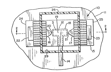
Fig. 1 ls a top plan vlew of an improved spar~ gap according
to the invention;
Fig. 2 is a cross sectional vlew taken alo~g line 2-2 of
Fig. 1; and
Fig. 3 is a vlew in cross section similar to Figure 2, but
lllustrating a mod~fied form of the invention.
~3~.5~
Best Mode For Carrvin~ Out The Inventlon
Referrlng to F~g~. 1 and 2 of the drawlnas, a solid state
spark gap device 10 i5 ~hown according to the inventlon. The
spar~ gap devlce 10 i8 ~or~ed on a dlelectrlc substrate 11, whlch
may be a ceramic ~ubstrate or the ~oundatlon used for normal
thick film circuit proces~lng techn'ques. ln the preferred
embodiment, the spar~ gap 10 device i8 formed from several layers
seguentially deposlted a~ thick fllms on the ~ubstrate 11. A
trigger electrode 12 is deposlted as a first layer. The trigger
electrode 12 ls formed from an electrically conductive material.
In the illustrated spark gap 10, the trigger electrode 12 has a
generally rectangular body 13 connected to a terminal 14.
However, it will be appreciated that the body 13 may have other
shapes.
A dlelectric second layer 15 ls deposited over the trigger
electrode body 13, an ad~acent portlon of the terminal 14 and a
predetermined ad~acent area on ~h~ substrate 11. The second
layer 15 18 ~ufficiently large to provide space for an anode 16
and a cathode 17. The d~electric second layer 15 is deposited
with a substantially uniform thlckness. Con~equently, the layer
15 will have a ralsed portion 18 where it extends over the thick
film forming the trigger electrode 12. The anode 16 and the
cathode 1~ are deposited as separate portions of a third layer on
the dielectric second layer 15. The anode 16 and the cathode 17
are electrically conductive layers deposited on the second lay~er
16 so as to lie opposite the substrate 11 and not opposite the
trigger electrode 12. The anode 16 and the cathode 1~ may be of
ldentical construction and are lnterchangeable ln electrical
connections to ad~oining circuitry. The anode 16 has a termlnal
end 22 and the cathode 1~ has a terminal end 23. The terminal
ends 22 and 23 may be on the second layer 15, as lllustrated, or
they may extend, re~pectively, over edge~ 24 and 25 of the ~econd
layer 15 and onto the sub~trate 11 for connecting directly to
other circultry ~not shoWn) on the substrate 11.
A spark gap 19 is formed between edges 20 and 21
f' ~ ~
re~pectively, of the anode 16 and the cathode 1~. The ~park gap
19 extends over the raised portlon 18 of the dielectric layer 15
and, hence, extend~ opposite th~ trig~er electrode 12. For many
applicatlons, the solid state spark gap device 10 will ~unction
adequately with no additional component~ or ~yers. However, the
device 10 must be located where the spar~ gap 19 i8 protected
from dust, moisture and other contaminations which may lower or
change the voltage required to break down the spark gap 19. If
the breakdown voltage i8 lowered, the spark gap 19 may discharge
prematurely.
If additional protection for the spark sap 19 18 desired or
required by ambient conditions, a cover 26 may enclose the spark
gap 19. An opt$onal fourth dielectric layer 27 may be deposited
to extend over a portion o~ the anode 16 and a por~lon of the
ad~acent second layer 15. However, the layer 2~ does not cover
the spark gap edge 20 or the terminal end 22 of the anode 16.
Similarly, an optional fourth dielectric layer 2B may be
deposited to extend over a portion of the cathode 1~ and a
portion of the ad~acent second layer 15. The layer 28 does not
cover the spark gap edge 21 or the terminal end 23 of the cathode
1~. The cover 26 may be fused or bonded to the fourth layers 27
and 28, the second layer 15 and the ~ubstrate 11 with, for
example, a sealing glas~ to form an enclosed chamber 29
surrounding the spark gap 19. Of course, the cover 26 may be
bonded in place by other means, such as by an epoxy resln. The
cha~ber 29 may be ~illed wlth dry air or with an lnert gas such
as nitrogen for maintaining controlled conditions at the spark
gap 19.
For operation o~ the spark gap device 10 in a flring clrcuit
(not shown), a predetermined potential i~ maintained between the
anode 16 and the cathode 17 by a charged capacltor. At the
proper time and conditions, a trigger pulse is applled to the
trigger electrode 12. The pulse on the trlgger electrode 12
produces ionization of some gas atoms in the spark gap 19,
thereby lowering the breakdown voltage across the spar~ gap 19 to
below the potentlal applied between the anode 16 and cathode 1~.
~3~6~3
- 6
When discharge take~ place acro~s the 3park gap 19, the energy
stored in the capacitor ~8 dumped to a load as a hlgh current
pulse of short duratlon. lt should be noted that the device lo
is particularly suitable for sin~le use applications, such as for
firing or initiating munltions. The solld state spark gap device
10 ls not de~igned ~or wlthstandlng ~park erosion which will
occur under continuous hi~h curre~t arc~ng.
It was stated above that the anode 16 and the cathode 1~ are
formed on the second layer 15 80 as ~ot to extend opposite the
trigger electrode 12 and that the spark gap 19 lies opposite the
trigger electrode 12. If the anode 16 and/or the cathode 1~
overlap the trigyer electrode 12, the electric field will be
concentrated in the portlons of the second layer 15 between the
overlapping anode 16 and/or cathode 1~ and trigger electrode 12.
(~ 15 As a consequence, a higher trigger voltage wlll be required to
~nltiate breakdown at the spar~ gap 19 becau~e any glven trigger
voltage will result in less lonization at the spark gap.
It will be appreciated that the solld Ytate spar~ gap device
10 may be manufactured using varlous known technologies. For
example, the device 10 may be manufactured by conventional thick
fllm processing techniques such as screen printing, drying and
flring. Or, the device may be ~anufactured using known processes
lnvolving the use of a photoresist and selective etching
techniques. Further, the spar~ gap device lo may be formed as an
integral element on a substrate which lncludes other circuitry,
or it may be formed as a separate element which can be connected
to other circuitry.
.
One optional construction i9 lllustrated in Fig. 3 where a
flrst conductive layer comprises the trlgger 30, anode 31, and
cathode 32 formed on the common ~ubstrate 34. These three
electrodes are electrlcally separated from one another, but are
~ormed at the same tlme on the ~ubstrate as one layer. A
precisely controlled dielectrlc 33 covers only the trigger 30 as
a second layer. The remaining construction would be as mentioned
above with the spark gap device of Fiyure 3 differlng from that
of Figures 1 and 2 in that the three electrodes 30, 31 and 32 are
,
,,
substantially coplanar allowlng for the elimi-~ation of one of the
layer forming step~ in the proce~s. Thu~, the opt~onal
dielectric layers 35 and 36 (which correspond to the fourth layer
2~ and 28 ~n Figure 2) are the third layer ln Figure 3.
Various other modificatlons and changes to the above
descrlbed preferred embodiment of the solid state spark gap
device 10 will be apparent to those ~kllled in the art wlthout
departing fro~ the spirit and the scope of the following claims.