Note: Descriptions are shown in the official language in which they were submitted.
2U349~4
PRINTER
BRIEF DESCRIPTION OF THE DRAWINGS
Fig. 1 is a block diagram showing the arrangement of
one embodiment of this invention. Fig. 2 is a block diagram
showing a reference circuit in the embodiment. Fig. 3 is a
S general explanatory diagram showing the memory arrangement in the
line buffers in the embodiment. Fig 4. is a detailed explanatory
diagram showing the memory arrangement in the line buffers in the
embodiment. Fig. 5 is an explanatory diagram showing reference
timing in the embodiment. Figs. 6(a) and 6(b) are explanatory
diagrams showing a conventional reference method. Figs. 6(c)
and 6(d) are explanatory diagrams showing the reference method
in the embodiment. Fig. 7 is a block diagram showing the
arrangement of a conventional printer. Fig. 8 is a circuit
diagram of a conventional thermal head. Fig. 9 is a flow chart
for a description of the operation of the conventional printer.
Figs. 10(a) - 10(h) are explanatory diagrams showing the data
patterns of dots surrounding an aimed dot in the conventional
printer. Figs. ll(a) - ll(j) are timing charts indicating
printing timing with respect to the data patterns shown in Figs.
lO(a) - 10(h). Fig. 12 is an explanatory diagram showing the
internal arrangement of the thermal head in the conventional
printer. Fig. 13 is a general explanatory diagram showing the
memory arrangement in the line buffer in the conventional
printer. Fig. 14 is a detailed explanatory diagram showing the
memory arrangement in the line buffer in the conventional
printer. Fig. 15 is a block diagram of one example of a
reference circuit in the conventional printer. Fig. 16 is an
2034964 ~
~2xplanatory diagram indicating reference timing in the
conventional printer.
RAC~ROUND OF THE lNV~N'l'lON
This invention relates to line printers, and more
particularly to the control of electrical energization of the
thermal head of a printer.
The arrangement of a conventional printer of this type
will be described with reference to Figs. 7 and 8.
Fig. 7 is a block diagram showing the arrangement of
the conventional printer, and Fig. 8 is a circuit diagram
showing the thermal head of the conventional printer.
The conventional printer, as shown in Fig. 7,
comprises: a CPU 1; a ROM 2 connected to the CPU l through a
bus; a RAM 3 connected to the bus; a parallel data input
interface 4; a counter connected to the bus and the parallel
data input interface 4; an input/output port 6 connected to the
bus and the parallel data input interface 4; a line buffer 7
connected to the parallel data input interface 4; a P/S
(parallel to serial conversion) circuit 8 connected to the line
buffer 7; a latch circuit 9 connected to the P/S circuit 8; a
latch circuit 10 connected to the latch circuit 9; a P/S
circuit 11 connected to the line buffer 7; a latch circuit 12
connected to the P/S circuit 11; a latch circuit 13 connected
to the latch circuit 12; a P/S circuit 14 connected to the line
buffer 7; a latch circuit 15 connected to the P/S circuit 14;
a latch circuit 16 connected to the latch circuit 15; a ROM 17
- 2034964
connected to those P/S circuits 8, 11 and 14 and latch circuits
9, 10, 12, 13, and 16; a switch circuit-18 connected to the ROM
17; an AND circuit 19 connected to the switch circuit 18 and
the latch circuit 15; a thermal head 20 connected to the AND
circuit 19; and a head temperature detecting circuit 21 whose
input and output are connected to the thermal head 20 and the
input/output port 6, respectively.
The thermal head 20, as shown in Fig. 8, comprises:
2048 heat generating resistance elements R1 through R2048; 32
0 shift registers LSINO.0 through LSINO.31; power t~rm;n~ls: a
CLOCK termi n~ l; and an HLTH t~rm; n~l .
Now, the operation of the conventional printer thus
constructed will be described.
Printing data are applied through the parallel data
input interface 4 to the line buffer 7. The data of an aimed
dot in a line to be printed is applied, as an output C3 of the
latch circuit 15, to the AND circuit 19. The data of the dot
before the aimed dot is applied as an output C2 to the ROM 17,
and the data of the dot after the aimed dot is applied as an
zo output C1 to the ROM 17.
The data of an aimed dot in the line before the line to
be printed is applied, as an output B3, to the ROM 17. The
data of the dot before the aimed dot is applied, as an output
B2, to the ROM 17, and the data of the dot after the aimed dot
2s is applied, as an output B1, to the ROM 17.
- 2034q64
The data of an aimed dot in the line which is located
two lines before the line to be printed is applied, as an
output A3, to the ROM 17. The data of the dot before the aimed
dot is applied, as an output A2, to the ROM 17, and the data of
the dot after the aimed dot is applied, as an output A1, to the
ROM 17.
The electrical energization time control of the thermal
head 20 will be described with reference to Fig. 9.
Fig. 9 is a flow chart for a description of the
electrical energization time control of the conventional
printer.
In Step S10, the CPU 1 detects the temperature of the
thermal head 20 with the aid of the head temperature detecting
circuit 21. The temperature detection data is stored in the
RAM 3.
In Step Sll, the printing interval of each line; that
is, a recording period is obtained, and stored in the RAM 3.
In Step S12, the real record dot number of a line to be
printed is obtained.
In Step S13, a degree of thermal effect on the printing
line is obtained according to the above-described recording
period and real recording dot number;
In Step S14, the above-described degree of thermal
effect is obtained for each of the first to current (present)
lines, and the degrees of thermal effect thus obtained are
stored.
2034964
In Step S15, a correcting value is obtained according
to the degrees of thermal effect thus stored and the head
temperature.
In Step S16, an electrical energization time is
obtained according to the head temperature and the recording
period, and the above-described correcting value is used to
obtain a flln~me~tal energization time Tl. In addition,
adjusting energization times T2, T3 and T4 are obtained
according to the outputs A1, A2, A3, B1, B2j B3, C1 and C2 of
lo the latch circuits, when necessary.
In Step S17, the thermal head 20 is energized according
to the fundamental energization time Tl and the adjusting
energization times T2, T3 and T4.
In Step S18, the above-described operations of Steps
Sll through S17 are carried out repeatedly until the printing
operation is accomplished.
The electrical energization time control will be
described with reference to Figs. 10 and 11 in more detail.
Fig. lO is an explanatory diagram showing the data
patterns of dots surrounding an aimed dot, and Fig. 11 is a
timing chart indicating printing timing with the data patterns
shown in Fig. 10.
The parts (a) through (h) of Fig. 10 shows eight
typical states of dots surrounding an aimed dot P in a line e
to be printed. In Fig. 10, reference characters ~-1 designates
the line before the line e to be printed; and Q-2 designates
_ 203496~
the line located two lines before the line Q. Furthermore, in
Fig. 10, hatched dots are to be printed black.
In the case of the part (a) of Fig. 10, the dots on
both sides of the aimed dot P, and the dots on the lines Q-1
and Q-2 are not printed. In this case, the heat generating
resistance element for the aimed dot P is not affected by the
heat of the other dots at all, and therefore the energization
time is the sum of the fundamental energization time T1 and the
adjusting energization times T2, T3 and T4 as-shown in the part
lo (j) of Fig. 11.
In the case of the part (b) of Fig. 10, the dot on the
left side of the aimed dot P is printed. In this case, the
heat generating resistance element for the dot affects the one
for the aimed dot P, and therefore in the total energization
time, the adjusting energization time T2 is off as shown in the
part (i) of Fig. 11.
In the case of the part (c) of Fig. 10, the heat
generating resistance element for the aimed dot P has printed
black dots on the preceding line Q-l. In this case, in the
total energization time, the adjusting energization time T3 is
off as shown in the part (h) of Fig. 11.
As can be estimated from the above description, in the
cases of the parts (d), (e), (f), (g) and (h) of Fig. 10, the
energization times are indicated in the parts (g), (f), (e),
(d) and (c) of Fig. 11, respectively. The parts (a) and (b) of
Fig. 11 show printing data, and latch signals, respectively.
- 6 -
A
- 2034964
In the above-described case, reference is made to dots
other than end dots of every data input of the thermal head 20
with eight reference dots of an aimed dot taken into account.
Now, a reference method in which reference is made to
5end dots of each data input of the thermal head will be
described with reference to Figs. 12 through 16.
Fig. 12 is an explanatory diagram showing separation of
the heat generating resistance elements of the thermal head 20
shown in Fig. 8. Fig. 13 and Fig. 14 are explanatory diagrams
oshowing the arrangement of memory in the line buffer 7. Fig.
15 is a block diagram showing a conventional reference circuit.
Fig. 16 is an explanatory diagram showing reference timing in
the prior art.
The 2048 heat generating resistance elements Rl through
5R2048 are connected to the serial in 64-bit shift registers
LSINO0 through LSINO31, and each of the data inputs HDI1
through HDI8 is handled by four shift registers; that is, each
data input has 256 bits.
For the purpose of high speed printing, two data inputs
20form an electrical energization block; that is, 512 bits can be
energized at the same time.
Thus, as shown in Fig. 8, the 2048 heat generating
resistance elements are divided into four energization blocks
HSBl, HSB2, HSB3 and HSB4.
25The thermal head 20 is designed as shown in Figs. 8 and
12. Therefore, the arrangement of memory of the line buffer 7
A
2034964
is allocated to data inputs of the thermal head 20, and in the
data inputs, the data corresponding to the heat generating
resistance elements Rl through R2048 are allocated as shown in
Fig. 14, being transferred, 8 bits by 8 bits, from the parallel
s data input interface 4.
As shown in Fig. 15, the conventional reference circuit
has two blocks equation in arrangement so that two data inputs
can be transferred simultaneously. One of the two blocks is
for the data inputs HDIl, HDI3, HDI5 and HDI7 of the thermal
head 20, and the other is for the data inputs HDI2, HDI4, HDI6
and HDI8.
The conventional reference method for an end dot of
each data input is such that, for instance in the case where
the aimed dot is R256 (Q) in Fig. 16, reference is made to only
five of the eight reference dots. Similarly, in the
conventional reference method, for an end dot of each data
input such as the aimed dot R257tQ) or R512(Q) reference is
made to five dots, for energization control.
As was described above, in the conventional printer,
for an end dot of each data input, reference is made to only
five of the eight reference dots to perform energization
control. Therefore, the resultant print includes a printing
defect such as a vertical stripe for every end dot.
2034~64
- SUMMARY OF THE INVENTION
Accordingly, an object of the invention is to
eliminate the above-described difficulty accompanying a
conventional printer. More specifically, an object of the
invention is to provide a printer which is improved in print
quality.
A printer according to the invention comprises the
following means:
(i) first storage means for storing at least data
on dots adjacent to an aimed dot on a line to be printed;
(ii) second storage means for storing data on aimed
dots on the line immediately before the line to be printed and
on the line located two lines before the line to be printed,
and at least data on dots adjacent to the aimed dots on the
line immediately before the line to be printed and on the line
located two lines before the line to be printed, the first and
second storage means storing data for at least eight dots;
(iii) third storage means for storing correcting
data formed according to the data stored by the first and
second storage means; and
(iv) control means for controlling the energization
time of the aimed dot on the line to be printed, according to
the correcting data, wherein the energization time of each dot
on the line to be printed, including each dot at opposite ends
of the line to be printed, is controlled by the control means
according to the correcting data formed based on the data for
at least eight dots.
~,~
In the printer of the invention, ~0 3 4 9 6 4
-
the first storage means stores at least data on dots
adjacent to an aimed dot on a line to be printed,
the second storage means stores the data on aimed
5 dots on the line immediately before the line to be printed and
on the line located two line before the line to be printed,
and at least data on dots adjacent to the aimed dots on the
line immediately before the line to be printed and the line
located two lines before the line to be printed,
the third storage means stores correcting data
formed according to the data stored by the first and second
storage means, and
the control means controls the energization time of the
aimed dot on the line to be printed, according to the
correcting data.
PREFERRED EMBODIMENT OF THE l~V ~:N'l'ION
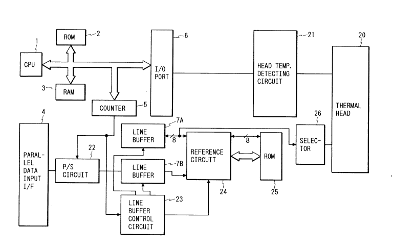
The arrangement of one embodiment of this invention
will be described with reference to Figs. 1 and 2.
Fig. 1 is a block diagram showing the arrangement of
the embodiment of the invention. In Fig. 1, reference numerals
1 through 6, 20 and 21 designate the same components as those
in Fig. 7 (the conventional printer).
The embodiment, as shown in Fig. 1, comprises: the
above- described CPU 1, ROM 2, RAM 3, parallel data input
interface 4, counter 5, input/output port 6, thermal head 20
2s and head temperature detecting circuit 21 which are the same as
those in Fig. 7; a P/S (parallel to serial conversion) circuit
22 connected to the parallel data input interface 4 and the
counter S; a line buffer control circuit 23 connected to the
counter 5; a line buffer 7A connected to the line buffer
control circuit 23; a line buffer 7B connected to the P/S
-- 10 --
. ;,~
:
- Z034964
circuit 22 and the line buffer control circuit 23; a reference
circuit 24 connected to the line buffers 7A and 7B and the line
buffer control circuit 23; a ROM 25 connected to the reference
circuit 24; and a selector 26 connected to the reference
circuit 24. The selector 26 is connected to the thermal head
20.
Fig. 2 is a block diagram showing the reference circuit
24 in the embodiment of the invention.
The reference circuit 24 comprises: a latch circuit 27
connected to the line buffer 7A; a latch circuit 9 connected to
the latch circuit 27; a latch circuit 10 connected to the latch
circuit 9; a latch circuit 28 connected to the line buffer 7A;
a latch circuit 12 connected to the latch circuit 28; a latch
circuit 13 connected to the latch circuit 12; a latch circuit
29 connected to the line buffer 7B; a latch circuit 15
connected to the latch circuit 29; and a latch circuit 16
connected to the latch circuit 15. Those latch circuits 27, 9,
10, 28, 12, 13, 29 and 16 are connected to the above-described
ROM 25. The line buffer 7A is connected to the latch
circuit 15.
In the above~described embodiment of the invention,
first storage means comprises the latch circuits 29, 15 and 16,
second storage means comprises the latch circuits 27, 9, 10,
28, 12 and 13, third storage means is the line buffer 7A, and
control means is the ROM 25.
203496~
The operation of the above-described embodiment will be
described with reference also to Figs. 3, 4, 5 and 6.
Printing data are applied through the parallel data
input interface 4 to the P/S circuit 22, where they are
s converted into serial data, which are applied to the line
buffer 7B (serial in serial out).
The data of an aimed dot on a line Q to be printed is
applied, as the output C3 of the latch circuit 15, to the line
buffer 7A. The data of the adjacent dot before the aimed dot
is applied, as an output C2, to the ROM 25, and the data of the
adjacent dot after the aimed dot is applied, as an output Cl,
to the ROM 25.
The data of~an aimed dot on the line before the line Q
to be printed is applied, as an output B3, to the ROM 25. The
data of the adjacent dot before the aimed dot is applied, as an
output B2, to the ROM 25, and the data of the adjacent dot
after the aimed dot is applied, as an output Bl, to the ROM 25.
The data of the aimed dot on the line located two lines
before the line to be printed is applied, as an output A3, to
the ROM 25. The data of the adjacent dot before the aimed dot
is applied, as an output A2, to the ROM 25, and the data of the
adjacent dot after the aimed dot is applied, as an output A1,
to the ROM 25.
As shown in Fig. 3, in each of the line buffers 7A and
2s 7B, the arrangement of memory is allocated to the data inputs
HDIl through HDI8 of the thermal head 20.
- 12 -
2034 964
The data Rl(Q) through R2048(Q) of the line Q to be
printed, corresponding to the heat generating resistance
- elements R1 through R2048 of each data input, the data Rl(Q-l)
through R2048(Q-1) of the line ~-1 before the line Q, the data
Rl(Q-2) through R2048(Q-2) of the line Q-2 located two lines
before the line Q, and the data of energization times T1, T2
and T3 (each of those data being provided twice for convenience
in arithmetic operation) are allocated as shown in Fig. 4,
because the correcting data of the P/S circuit 22, the
reference circuit 24 (the output C3 of the latch circuit 15)
and the ROM 25 are provided in serial manner.
Fig. 5 shows reference timing employed in the
embodiment. The correcting data (energization times T1, T2 and
T3) for the line to be printed are formed according to a
reference method as shown in Figs. 6(c) and 6(d), and stored
in the line buffer 7A. In the case where the aimed dot P is
R256, the reference dots are made up of eight dots with the dot
R257 of the next data input HDI2 being inclusi~e, and the
energization time pattern (corresponding to the data stored in
the ROM 25 in ad~ance) is determined from the pattern
(corresponding to the addresses in the ROM 25) of the reference
dots. Similarly, in the case where the aimed dot P is R257 or
R512, the reference dots are made up of eight dots, and the
energization time pattern is determined from the pattern of the
reference dots. When provision of the energization time
pattern has been accomplished for one line (HDI1 through HDI8)
Z03496~
_, .
the energization control is started. The energization time is
determined in the same manner as in the prior art; that is, the
determination is carried out as shown in Fig. 9. However, in
this case, the adjusting energization time T4 is not used.
S As was described above, in the embodiment of the
invention, the energization time is controlled with the effect
of heat of eight reference dots taken into account even for the
end dot of each data input, with the result that the print
quality is remarkably improved.
lo The embodiment has been described with reference to the
thermal head of eight-inputs and four energization blocks;
however, the technical concept of the invention can be equally
applied to other thermal heads having more inputs and more
energization blocks.
The reference dots may be dots adjacent to the aimed
dots on the line immediately before the line to be printed and
the line located two lines before the line to be printed. And
not only the dots on the right and left side of the aimed dot,
but also the dots next to those dots can be employed as
reference dots, to achieve the object of the invention.
In the above-described embodiment, three different
energization times Tl, T2 and T3 are employed for the
energization control of the aimed dot; however, the invention
is not limited thereto or thereby. That is, the same effect
2s can be obtained by employing a variety of energization time
patterns.
- 14 -
2034964
As was described above, the printer of the invention
comprises: the first hold means for holding at least data on
dots adjacent to an aimed dot on a line to be printed; the
second hold means for holding data on aimed dots on the line
immediately before the line to be printed and on the line
located two line before the line to be printed, and at least
data on dots adjacent to the aimed dots on the line immediately
before the line to be printed and the line located two lines
before the line to be printed; the third hold means for holding
o correcting data formed according to the data held by the first
and second hold means; and the control means for controlling
the energization time of the aimed dot on the line to be
printed, according to the correcting data. Hence, the printer
of the invention is considerably high in print quality.