Note: Descriptions are shown in the official language in which they were submitted.
2~3~10~
A-52472/ESW
COL~IMATED DEPOSITION APPARATU~ AND M~THOD
Field of the Invention
This invention pertains generally to sputter
coating and, more particularly, to apparatus and a
method for depositing a step coating on a workpiece by
sputtering.
Backqround of the Invention
Sputter coating is commonly employed in the
formation of films on substrates in the manufacture of
semiconductor devices, and planar magnetrons have long
been used as sputtering devices to coat silicon wafers
with various materials, such as aluminum, during the
manufacture of integrated circuits.
With sputter coating, it is di~ficult to form a
uniform thin film, or step coating, which conforms to
the shape of a workpiece where a step occurs, e.g. at
the upper or lower corner of an opening such as a hole
or a via in the surface of a woxkpiece. It is also
difficult to fill small openings (e.g. one micron, or
less, in diameter or width) and tc provide controlled
film growth on the side and bottom walls of such
openings~ These difficulties arise because particles
tend to leave the source in all directions, then collide
with each other and scatter, arriving at the workpiece
from a variety of angles. Particles which arrive at
angles greater than about 45 deyrees fro~ normal to the
workpiece surface tend to produce lateral growth on the
surface, rather than impinging upon the walls of the
203510~
--2
openings. ~his lateral growth can result in overgrowth
at the tops of the openings which can eventually close
off the openings and prevent the particles from entering
the openings.
Ob;ects an~ ~ummarv of the Invention
It is in general an object of the invention to
provide a new and improved sputtering apparatus and
method for coating a workpiece.
Another object of the invention is to provide
apparatus and a method of the above character which
overcome the limitations and disadvantages of sputtering
systems heretofore provided.
Another object of the invention is to provide
apparatus and a method of the above character which are
particularly suitable for use in forming step coatings.
These and other objects are achieved in accordance
with the invention by supporting a workpiece in a
chamber, emitting particles from a sputter source
substantially uniformly throughout an area of greater
lateral extent than the workpiece, maintaining the
pressure within the chamber at a level which is
sufficiently low to prevent substantial scattering of
the particles between the source and the workpiece, and
passing the particles through a particle collimating
filter having a plurality of transmissive cells with a
length to diameter ratio on the order of 1:1 to 3:1
positioned between the source and the workpiece to limit
the angles at which the particles can impinge upon the
workpiece.
Brief DescriP~ion of the Drawinas
FIG~ 1 is a diagrammatic cross-sectional view of
one embodiment of sputtering apparatus incorporating the
invention.
~3~
FIG. 2 is a top plan view, on a reduced scale, of a
particle collimating filter for use in the embodiment of
FIG. 1.
FIGS. 3a-3b are fragmentary cross-sectional views
illustrating some of the problems encountered in the
formation of a step coating with conventional sputtering
techniques.
FIGS. 4a-4d are graphical representations showing
the relationship between pressure and the angular
distribution of particles arriving at the surface of a
workpiece with collimating filters of different aspect
ratios.
FIG. 5 is a graphical representation showing the
relationship between side wall deposition rate and
aspect ratios of holes or vias and collimating filters.
FIGS. 6a-6d are graphical representations showing
the relationship between bottom wall deposition rate and
aspect ratios of holes or vias and collimating filters.
FIG. 7 is a graphical representation showing the
combined bottom and side wall deposition rates in a hole
or via utilizing a collimating filter in accordance with
the invention.
FIG. 8 is a graphical representation showing
relative side and bottom wall coverages obtained with
collimating filters of different aspect ratios.
FIGS. 9a-9b are fragmentary cross-sectional views
of a workpiece, illustrating the formation of a step
coating with the apparatus and method the inv~ntion.
FIG. 10 is a view similar to FI~S. 9a-9b,
illustrating the formation of another step coating with
the apparatus and method the invention.
FIG. 11 is a graphical representation illustrating
the temperature conditions and depostion rates utilized
in obtaining the coating of FIG. lOo
FIGS. 12-14 are diagrammatic cross-sectional views
of additional embodiments of sputtering apparatus
incorporating the invention.
203~1~6
FIG. 15 is a diagrammatic top plan view of another
embodiment of a collimating filter for use in sputtering
apparatus incorporating the invention.
Detailed Description
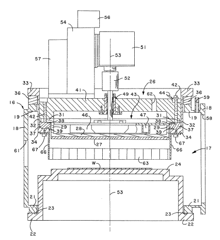
In the embodiment of FIG. 1, the sputtering
apparatus has a housing 16 in which a sputtering chamber
17 is formed. The housing includes a cylindrical side
wall 18 with annular flanges 19, 21 toward the upper and
lower ends thereof, and a bottom wall 22 which mates
with flange 21. An O-ring 23 provides a seal between
the two walls.
The central portion of bottom wall 22 is raised to
form a table 24 for supporting a wafer W or other
workpiece to be coated. The workpiece is secured to the
table by suitable means such as a peripheral clamping
ring tnot shown). The table includes conventional
heating means (not shown) for controlling the
temperature of the workpiece.
The housing and support table are fabricated of an
electrically conductive material such as stainless steel
and are connected electrically to ground.
A source 26 of particles for coating the workpiece
is mounted in the upper portion of housing 16. In the
embodiment illustrated, the source is a rotating
magnetron source of the type described in detail in
Serial No. , filed January 26, 1990, and
entitled "Rotating Sputtering Apparatus for Selected
Erosion". An important feature of this source is that
is provides a substantially uniform emission of
particles over an extended target area which is larger
than the workpiece. This ensures that a uniform
distribution of particles reaches the entire surface of
the workpiece, including the peripheral areas. While
this particular source is presently preferred, any other
source which provides a similar particle distribution
can be employed.
~3~
Source 26 includes a circular target 27 of aluminum
or other material to be deposited. The target is
disposed in parallel facing relationship to the
workpiece and is of greater lateral extent than the
workpiece. ~ith a wafer having a diameter of 8 inches,
for example, the target can have a diameter of 11.25
inches.
The target is mounted on the under side of an
electrically conductive cathode plate 28 which has a
cylindrical side wall 29 with an annular flange 31 at
the upper end thereof. The cathode plate is supported
by a cylindrical mounting bracket 32 with annular
flanges 33, 34 at the upper and lower ends thereof.
Flange 33 projects outwardly from side wall 29 and is
positioned above the inwardly projecting housing flange
19. A spacer ring 36 is positioned between these
flanges to permit adjustment of the spacing between the
target and the workpiece, which is typically on the
order of 1-3 inches.
Flange 31 on the cathode plate projects outwardly
from side wall 29 and is positioned above the inwardly
projecting flange 34 at the lower end of mounting
bracket 32. An ring 37 of electrically insulative
material is positioned between the flanges to insulate
the cathode from the housing, and o-rings 38, 39 provide
seals between the flanges and the insulator.
A cover 41 fabricated of an insulative material
such as fiberglass is positioned within mounting bracket
32 and secured to flange 31 of the cathode plate by
screws 42 to form a chamber 43 for the rotating magnet
assembly of the magnetron. An electrical lead 44 is
connected to one of the mounting screws 42 and to a
suitable source (not shown) for applying a high negative
potential to the cathode.
The magnet assembly includes a housing 46 in which
an array of magnets 47 is mounted. The structure of
these magnets and the manner in which ~hey provide
2 ~
substantially uniform erosion over substantially the
entire area of the target are disclosed in detail in the
aforementioned Serial No. , and that disclosure
is incorporated herein by reference.
Magnet housing 46 is mounted on a shaft 48 which
passes through a seal assembly 49 in cover 41 and is
connected to a motor 51 by a coupling 52 ~or rot~tion
about an axis 53. Motor 51 is mounted on a slider
assembly 54 which is driven by a linear motor 56 for
movement along axis 53, and the slider assembly is
mounted on a bracket 57 affixed to housing 16. The
slider assembly permits the spacing between the magnet
array and the target to be adjusted to control the
magnetic field beneath the target. As discussed more
fully in the aforementioned Serial No. , with an
11.25 inch target, the rotating magnet array provides
substantially uniform erosion throughout a circular
reyion having a diameter of approximately 10 inches
centered about the axis of rotation, which is sufficient
for coating an 8 inch wafer.
Housing 16 includes a port 58 to which a vacuum
pump ~not shown) is connected for evacuating chamber 17,
and a gas inlet 59 through which an inert gas such as
Argon is introduced to support the magnetron discharge.
As discussed more full~v ~ereinafter, the pressure within
the chamber is maintained at a pressure which is
sufficiently low to prevent the sputtered particles from
colliding with each other and scattering. Suitable
pressures for this purpose are on the order of 0.1-1.5
milliTorr.
The housing also includes a port 61 through which
wafers or other workpieces are transported into and out
of chamber 17. This port is provided with a suitable
closure such as a gate valve (not shown).
A port 62 is provided in co~er ~1 for introducing a
coolant such as water into chamber 43 to cool the target
and the magnet assembly.
~3~10~
A particle collimating filter 63 is positioned
between the target and the workpiece to limit the angles
at which the particles from the source can arrive at the
surface of the workpiece. This filter, together with
the extended source and the absence of scattering, i5
important in preventing lateral film growth and in
forming a step coating with controlled growth on the
bottom and side walls of an opening such as a hole or
via.
The collimating filter has a plurality of cells 64
with apertures through which the particles pass in line-
of-sight fashion. The cells are aligned with their axes
parallel to axis 53 and perpendicular to the surfaces of
target 27 and workpiece W. Each cell has an acceptance
angle eACC which is defined as
eAcc = arctan (d/l),
~here d is the diameter of the aperture and l is the
length of the aperture, or the height of the cell. The
acceptance angle is thus the maximum angle from the
~0 perpendicular at which particles can pass through the
filter without striking the wall of a cell. The aspect
ratio of the cells, i.e. the ratio of the cell height to
the diameter, is referred to as the aspect ratio of the
filter.
In the embodiment illustrated, the cells and their
apertures are hexagonal in cross-section. This shape is
preferred to a circular shape or a square shape because
of the unusable areas between the walls of adjacent
circular cells and the substantial difference in the
distances between the opposing sides and the opposing
corners of square cells. In this disclosure, the
diameter utilized in defining the accept~nce angle and
the aspect ratio of the hexagonal cells is the mean
diameter of the cells, although either the flat-to-flat
diameter or the apex-to-apex diameter could be utilized
for this purpose, if desired.
2~3~
In the embodiment of Figure 1, the collimating
filter is positioned midway between the target and the
workpiece and is attached to mounting bracket 32 by
brackets 66 and screws 67.
The filter has an aspect ratio on the order of 1:1
to 3:1, with a mean cell diameter on the order of 3/8
inch for an 11.25 inch target and an 8 inch wafer
separated by a distance on the order of 1-3 inches.
FIG. 3a illustrates some of the problems
lo encountered in forming a step coating by sputtering
prior to the invention. In this example, a hole 71
having a diameter on the order of one micron is formed
in a one micron layer 72 of dielectric material on a
silicon substrate 73, and a metallized contact is to be
formed over a doped region 74 in the substrate at the
bottom of the hole. The metallization particles are
sputtered from a target 75 above the wafer. Each point
on the target emits particles with a cosine
distribution, and after collision and scattering, the
particles arrive at the target at angles (e) ranging
from 0 to 9o degrees to the normal.
Particles arriving at angles greater than 45
degrees cannot impinge upon the bottom wall of the hole
and tend to promote lateral growth on the surface of the
wafer. As a result, a relatively thick film 76 is built
up on the surface of the wafer, with relatively thin,
nonuniform coatings 77, 78 on the side and bottom walls
of the hole. In addition, the lateral growth of the
surface film produces an overgrowth 79 at the top of the
hole, which can close off the hole completely and
prevent particles from entering it. The coating on the
side walls and the bottom wall is subject to voiding, as
illustrated by broken lines in the drawing, and there
can even be areas where no coating is formed.
FIG. 3b illustrates a problem of asymmetrical
coating which occurs in openings near the edge of a
wafer with conventional sputtering techniques utilizing
~03~1 ~6
a 11.25 inch planar source, a surface deposition rate of
1 micron per minute, a target to wafer spacing of 7 cm,
a sputtering pressure on the order of 3-7 milliTorr, and
a wafer table temperature of 250 deg. C. In this
figure, two holes 81, 82 are shown. Hole 81 is near the
center of the wafer, and hole 82 is near the edge. Near
the center of the wafer, the particle distribution is
relatively uniform, and a relatively symmetrical coating
is formed in hole 81. Toward the edge of the wafer,
however, the distribution of particles is not as
uniform, and the inwardly facing side wall 82a of hole
82 receives more particles than the outwardly facing
wall 82b. This results in an asymmetrical coating of
the side walls as well as the bottom wall.
With the collimation filter, the extended source,
proper selection of pressure, and proper selection of
the aspect ratio of the filter, it is possible to form
good step coatings in which the growth of film on the
side and bottom walls of an opening is controlled, and
with proper temperature control, it is even possible to
achieve planarization of the metallized coating over the
opening.
FIGS. 4a-4d illustrate the effect of pressure on
the angular distribution of particles arriving at the
surface of the workpiece for filters of different aspect
ratios. In the figures, the angle of arrival (e) is
plotted along the x-axis and the number of particles
arriving at the surface is plotted along the y-axis.
The data for these figures was obtained by computer
simulation assuming uniform erosion from an 11 inch
planar source, with a 150 mm substrate and a 9 cm source
to substrate spacing in the Argon sputtering of
aluminum. In each figure, curves representing the
distributions for operating pressures of .0005 milli-
Torr, .02 milliTorr, .5 milliTorr and 1 milliTorr are
shown, and in FIGS. 4b-4d a curve for a pressure of
2 milliTorr is also shown.
~3~
--10--
FIG. 4a shows the di~tribution with no filter, and
FIGS. 4b-4d show the distributions with filters having
aspect ratios of 1:1, 1.5:1 and 2:1, respectively.
Without the filter, the distribution is fairly
symmetrical at the lower pressures for angles up to
about 60 degrees. At the higher pres~ures, the
distribution is less symmetrical, and greater relative
numbers of the particles arrive at angles greater than
60 degrees.
With each of the filters, the distribution is
fairly symmetrical at the lower pressures up to the
acceptance angle of the filter. At the higher
pressures, the distribution is less symmetrical, and
greater relative numbers of the particles arrive at
angles greater than the acceptance angle. The increase
in the number of particles outside the acceptance angle
at the higher pressures is due to scattering of the
particles at the higher pressures, and these curves
illustrate the importance of lower pressures to avoid
scattering and keep as many particles as possib.e within
the acceptance angle of the filter.
FIG. 5 illustrates`the relationship between rate of
deposition on the side wall and the aspect ratios of
holes or vias and collimating filters. The aspect
ratios of the openings (i.e. depth/diameter) are plotted
along the x-axis, and the initial rate of the side wall
deposition normalized to the deposition on the surface
of the wafer is plotted along the y-axis. This
normalized value is of interest in that it gives the
fractional unit of thickness on the side wall for a unit
of thickness on the surface. In this figure, the target
is assumed to be sufficiently large that the location of
the opening on the wafer is unimportant. Curves are
shown for filters having aspect ratios ranging from
0.5:1 to 2.5:1.
From FIG. 5, it can be seen thaL filters having
aspect ratios of 0.5:1 and 1:1 give fairly uniform side
'~3~
wall coatings for openings having aspect ratios up to
about 1:1, with the 1:1 filter giving a substantially
thicker coating than the 0.5:1 filter. With filters
having higher aspect ratios, the wall coating thickness
drops rapidly as the aspect ratio of the hole increases
up to about l:l. Thereafter, the thickness continues to
decrease rapidly as the aspect ratio increases,
approaching zero at a ratio of 3:1.
FIGS. 6a-6d illustrate the relationship between the
initial deposition rate on the bottom wall and the
aspect ratios of holes or vias and collimating filters.
In these figures, distance from the center of the hole
or via expressed as a fraction of the radius of the hole
or via is plotted along the x-axis, and the rate of
deposition on the bottom wall normalized to the rate of
deposition on the surface of the wafer is plotted along
the y-axis. As in the previous figure, the target is
assumed to be sufficiently large that the location of
the opening on the wafer is unimportant. Curves are
included for holes having aspect ratios ranging from -
0.25:1 to 2:1. FIG. 6a shows the relationship without a
collimating filter, and FIGS. 6b-6d show the
relationship for filters having aspect ratios of l:l,
2:1 and 4:1, respectively.
With no filter and a hole having an aspect ratio of
1:1, the coating is full thickness toward the center of
the opening but only about half thickness near the wall.
With a filter having an aspect ratio of l:l, the coating
on the bottom wall is substantially more uniform,
ranging from a normalized value of about .70 toward the
center to about .40 near the wall. The bottom coating
is even flatter with filters having aspect ratios of 2:1
and 4:1, but it is also substantially thinner.
With no filter and a hole having an aspect ratio of
2:1~ the bottom coating varies in thickness from a
normalized value of about .60 toward the center to about
.30 near the wall. With a filter having an aspect ratio
2~3~10~
of 1:1, the coating is more uniform, ranging from a
normalized thickness of about .26 near the center to
about .20 toward the wall. With a 2:1 filter, the
coating is even more uniform, with a normalized
thickness of about .13 from the center to the wall.
Thus, FIGS. 6a-6d illustrate the desirability of
utilizing a filter with the same aspect ratio as the
opening in order to provide uniformity in the coating on
the bottom wall of the opening.
FIG. 7 illustrates the combined effects the
invention on side wall coating and bottom wall coating
for an opening and a collimating filter each having an
aspect ratio of 1:1. This figure is similar to
FIGS 6a-6d in that the distance from the center of the
hole is plotted along the x-axis, and the thickness of
the bottom wall deposition normalized to the deposition
on the surface of the wafer is plotted along the y-axis.
A curve 83 taken from FIG. 6b shows the bottom wall
thickness for a hole and a filter having an aspect ratio
of 1:1, and a curve 81 taken from FIG. 5 shows the
coating on the side wall for a hole and a filter with
this aspect ratio. In the area in the bottom corner of
the opening designated by the reference numeral 85,
there is an overlap of the coatings formed on the side
wall and on the bottom wall, and the excess material
from this area builds up in the area 86, forming a
radius at the corner of the coating.
FIG. 8 illustrates the relative side and bottom
wall coverages obtained in holes ranging from about 1 to
2 microns in diameter with collimating filters having
aspect ratios of 1:1 and 0.67:1. In this figure, the
hole size is plotted along the x-axis, and the ratio of
the wall thickness to the surface film thickness is
plotted along the y-axis. The data shown in this figure
was obtained experimentally from the deposition of
aluminum containing 1~ silicon at a temperature of
loO deg. C and a sputtering pressure ~f 1 milliTorr.
~3~
-13-
This data confirms a bottom wall to side wall thickness
ratio of about 6 to 1, which is in accord with
simulations represented in the other figures.
FIGS. 9a-9b illustrate the formation of a step
coating when the apparatus and method of the invention
are employed. Each of these figures shows a pair of
holes 88, 89 having aspect ratios of 1:1, with hole 88
being located near the center of a wafer and hole 89
being toward the edge. Sputtering is performed at a
pressure of .5 milliTorr and a wafer table temperature
of 250 deg. C, with an 11.25 inch planar source, a 7 cm
target to wafer spacing, a collimation filter having an
aspect ratio of 1:1, and a surface deposition rate of
1 micron per minute.
FIG. 9a shows a half thickness coating of .5 micron
on the wafer surface, and FIG. 9b shows a full thickness
coating of 1 micron on the surface. The figures
illustrate how the coating builds up evenly on the side
walls of the openings without the overcoating and
asymmetry of the prior art techniques illustrated in
FIGS. 3a-3b. Another advantage of the invention which
is apparent from these figures is that the thinnest part
of the step coating is no longer at the lower corner of
the hole as it is in the coatings of FIGS. 3a-3b. With
the half thickness coating, the thinnest point occurs
along the side wall, as indicated by the arrows 91, and
with the full thickness coating, it occurs at the upper
corner of the hole, as indicated by the arrows 92. From
these figures, it can also be noted that the aspect
ratio of the unfilled volume increases as the coating
builds up in the holes.
FIG. 10 illustrates a coating which is produced
utilizing the same operating parameters as in the
examples of FIGS. 9a-9b, except that the temperature of
the wafer is controlled in the manner illustrated in
FIG. 11~ In this examp'e, the temperature of the wafer
table is monitored with a thermocouple, and the
2~3~
-14-
temperature of the wafer is monitored with a non-contact
sensor. In FIG. 11, temperature is plotted as a
function of time, with curves 93, 94 showing the wafer
table and wafer temperatures, respectively.
As illustrated in FIG. 11, the wafer is preheated
initially to a temperature on the order of 100-125 deg.
C for a period of 10 minutes, following which the
temperature is held constant and sputtering begins at a
rate of 1000 Angstroms per minute for one minute. ~n
additional 1000 Angstroms is deposited in a period of 15
minutes. Thereafter, the sputtering rate is increased,
and 8000 Angstroms is deposited while the temperature is
ramped up to a level of 260-360 deg. C over a period of
about 12 minutes. The resulting coating 96 fills the
holes completely and exhibits good planarization above
the holes at both the center and the edge of the wafer.
FIG. 12 illustrates an embodiment of the invention
which is suitable for either sputtering or etching or
for simultaneous sputtering and etching of a substrate.
This embodiment is similar to the embodiment of FIG. 1
except that the bottom wall and wafer support table are
replaced with a second magnetron assembly 111 which is
similar to source 26 but is mounted in an inverted
position with the wafer or workpiece W mounted on its
cathode plate 112 in place of a target. As in the
embodiment of FIG. 1, housing 16 is grounded and a high
negative DC voltage is applied to the cathodes.
Particles are sputtered from the target on the upper
magnetron and from the wafer on the lower magnetron.
Thus, the surface of substrate W is simultaneously
sputter coated by particles dislodged from the surface
of target 27 by the operation of the upper magnetron and
sputter etched by the particles dislod~ed from the
surface of the substrate by the operation of the lower
magnetron.
A particle collimating filter 63 is mounted on the
upper magnetron and is positioned midway between the
2~3~0~
-15-
target and the workpiece to control the angles at which
the particles from the target impinge upon the workpiece
as in the embodiment of FIG. l.
The embodiment of FIG. 13 is similar to the
embodiment of FIG. 1 except that the collimating filter
63 is movable in a direction parallel to the surfaces of
the target 27 and the workpiece W, rather than being
mounted in a fixed position relative to the target and
workpiece. The filter is mounted on a shaft 116 which
can be rotated back and forth a small amount about an
axis 117 which is spaced from the axis 53 of the
magnetron. With the filter mounted in a stationary
position, there may be some shadowing or shading whereby -
the walls of the cells create areas on the warkpiece
which are blocked from line of sight transmission from
the target, and these areas may receive less coating
than the rest of the workpiece. By moving the filter a
distance corresponding to about one half of the diameter
of a cell, the shadowing or shading is eliminated. If
desired, a translational motion or an axial motion can
be utilized instead of a rotational motion to eliminate
the fine structure produced by shadowing. With these
alternative motions, a movement of about one half of the
cell diameter is still sufficient to eliminate the fine
structure. This represents a significant improvement
over prior art techniques in which the wafer is moved,
and movement on the order of the diameter of the wafer
is necessary. The movement of the filter is
particularly effective if the filter is positioned as
close to the wafer surface as possible.
FIG. 14 illustrates an embodiment of the sputtering
apparatus in which the aspect ratio of the collimating
filter can be changed during a coating operation. As
noted above, it is desirable to match the aspect ratio
of the filter to that of the opening being coated, but
the aspect ratio of the unfilled volume continually
increases as the opening is filled. By increasing the
o ~
aspect ratio of the filter, the desired match can be
maintained.
In the embodiment of FIG. 14, filter 63 i5 formed
in two sections 63a and 63b which are mo~able axially
5 relative to each other, and the aspect ratio is changed
by changing the spacing between the sections, which
effectively changes the height of the cells. The two
sections are brought together at the start of a coating
operation, and as the deposition progresses and the
10 aspect ratio of the opening changes, the sections are
separated to keep the aspect ratios approximately equal.
FIG. 15 illustrates another embodiment of a
collimating filter which permits the aspect ratio of the
filter to be changed as the deposition progresses. In
15 this embodiment, the filter is in the form of a wheel
121 having a plurality of filter sections 122-126 of
different aspect ratios. In the embodiment illustrated,
the cells in sections 122-126 have aspect ratios of 1:1,
1.5:1, 2:1, 2.5:1 and 3:1, respectively. The wheel is
20 adapted for rotation about an axis 128 spaced from the
axis 53 of the magnetron to bring successive ones of the
filter sections into position between the target and the
workpiece.
Rather than changing the aspect ratio of the
25 filter, the effect of the increasing aspect ratio of the
unfilled volume can also offset by using a filter having
a substantially greater aspect ratio than the hole, e.g.
a filter having an aspect ratio of 1.5:1 or 2:1 for a
hole having an aspect ratio of 1:1, starting the
30 deposition at a pressure substantially higher than the
preferred pressure for a feature having the aspect ratio
of the hole, and reducing the pressure as the deposition
progresses. With the 1:1 aspect ratio, for example, the
pressure might start at a level of 1.5 milliTorr and be
35 reduced to a level of 0.5-1.0 milliTorr as the
deposition progresses.
2~3~
It is apparent from the foregoing that a new and
improved sputtering apparatus and method have been
provided. While only certain presently preferred
embodiments have been described in detail, as will be
apparent to those familiar with the art, certain changes
and modifications can be made without departing from the
scope of the invention as defined by the following
claims.