Note: Descriptions are shown in the official language in which they were submitted.
203~55
NT23
S P E C I F I C A T I 0 N
LINEAR TRANSMITTER
[ Technical Field ]
This invention relates to a transmitter for radio
frequency (RF). It relates, more particularly, to a linear
transmitter which amplifies and transmits modulated signals
of which envelope changes greatly in the signal level at a
high power efficiency.
[ Background Technology ]
There has been used a power amplifier of class A or B
as the linear transmitter for radio frequency. But such
power amplifier is defective in that the power efficiency
remarkably deteriorates in the low level region when it is
used to amplify modulated signals which changes drastically
in the level of envelope. In RF transmitters of portable
type which uses batteries as the power source, for example,
such problems arise as duration of transmittable time be-
comes short or a large and heavy battery becomes necessary.
In order to overcome such problems, the present
applicant has filed a patent application for the linear
power amplifier of high efficiency (Japanese Patent Applica-
tion laid-open Sho 62-274906). FIG. 1 shows the construction
of an embodiment of the linear transmitter using above-
mentioned linear power amplifier.
An input terminal 1 is inputted with signals to be
,~
~0~5~5~
modulated in analog or digital form. A modulator 2 generates
linear modulated signals based on the above signals. A
high-frequency saturated power amplifier 4 amplifies the
linear modulated signals and outputs the same at an output
terminal 9.
The power amplifier 4 includes an input matching
circuit 41, an FET 42 as an amplification device, a RF choke
coil 43 and an output matching circuit 44, and makes the
saturated output level of the amplifier 4 correspond to the
envelope of the input signals by controlling the drain bias
voltage V of the FET to be substantially proportional to
the envelope of the input signals. This type of control
enables the amplifier 4 to operate as a linear amplifier
while maintaining it at saturation condition with a high
efficiency to remarkably reduce the distortion in outputs.
The drain bias voltage V may be obtained by con-
trolling the power voltage inputted at a power supply termi-
nal 8 by a DC voltage controller 7. The DC voltage control-
ler 7 includes a DC-DC converter or a series-pass regulated
transistor, and is controlled by drain voltage control
ignals V . The control signals V are obtained by dividing
C C
with a coupler 3 the linear modulated signals fed from the
modulation 2 to the amplifier 4, detecting the envelope
thereof with an envelope detector 5 and compensating the
detector output V ' using a compensate circuitry 6.
As the above-mentioned prior art uses a saturatiOn
2~354~
type radio frequency power amplifier of high efficiency,
theoretically it can conduct linear amplification at a
remarkably high efficiency. For instance, if an saturated
power amplifier of power efficiency of 70% as the amplifier
4 and a DC-DC converter of 75% as the circuit 7 are used,
the linear amplification may be conducted at combined effi-
ciency of 50% or higher.
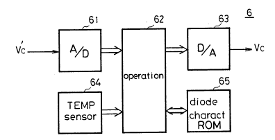
FIG. 2 is a block diagram to show an embodiment of
the compensate circuitry 6.
An envelope detector 5 includes a RF diode or other
parts of non-linear analog circuit, and characteristics of
detector thereof change due to changes in temperature. The
current temperature is detected by a temperature sensor 64,
and the detector output V of the detector 5 is compensated
based on the temperature by an operational circuitry 62.
The detector output V ' is digitized by an A/D con-
verter 61 and inputted at an operational circuitry 62. Thecircuitry 62 reads a compensating value for the diode char-
acteristic which corresponds to the output of the tempera-
ture sensor from a memory 65 which stores diode characteris-
tics and compensates the input signals with the compensated
values. The result is converted into analog signals by D/A
converter 63 and outputted.
However, the prior art linear transmitter fluctuates
in its detector characteristics by temperatures changes as
well as manufacture errors as the envelope detector com-
prises RF diode or other parts of non-linear analog cir-
- 203~5~
cuit. Therefore, the drain control signals are extremely
difficult to improve their precision, and errors in drain
bias make it difficult to reduce distortion satisfactorily.
This problem may be solved by providing a compensate
circuitry, but the construction of such the circuitry
inevitably becomes more complicated and expensive.
This invention aims to overcome those problems en-
countered in the prior art and aims to provide a linear
transmitter which can conduct linear power amplification at
high efficiency with less distortion but without the neces-
sity to use complicated compensate circuitries.
[ Disclosure of the Invention ]
The linear transmitter according to this invention
has a modulation unit comprising a complex envelope genera-
tor which generates in-phase envelope signal component and
quadrature envelope signal component of modulated signals
out of the input signals, a quadrature modulator which
generates modulated signals out of the in-phase envelope
signal component and quadrature envelope signal component,
and an envelope generating means which obtains envelope from
both of the envelope components and supplies the same to a
bias means.
Instead of obtaining envelopes with an envelope
detector having diodes or other analog devices in radio
frequency, it obtains envelopes by digital arithmetic proc-
essing in the base band. This resolves the problem of char-
acteristic fluctuation which is otherwise caused in analog
21~4!~
devices.
Moreover, as drain (or collector) control signals are
obtained by digital arithmetic processing, highly stable and
precise control signals can be obtained without the necessi-
ty of adjustment to attain sufficient effect in distortion
reduction. Further, it facilitates construction of LSI
circuits.
The envelope generating means may include a numerical
arithmetic processor which obtains envelopes from the input
in-phase envelope component and quadrature envelope compo-
nent by digital arithmetic operation. It may separately
include a memory table which outputs values that have been
written in for the in-phase envelope component and quadra-
ture envelope component.
It is preferable to provide a delay time adjustment
means which matches timewise the waveforms of the modulated
signals inputted at the radio frequency power amplifier with
the waveforms of the bias voltage in order to compensate the
time delayed by digital processing.
It may include an frequency equalizer which equalizes
the output amplitude and phase of the envelope generating
means and supplies them to a bias means. This can enhance
the bandwidth of frequency characteristics of the bias means
to be sufficient for high modulation frequency.
It may include a minimum bias voltage hold means
which maintains the output voltage from the bias means at a
prescribed value or higher when the signal level of the
envelope outputted from the envelope generating means is
`-- 2 ~) 3 ~
smaller than a preset level. This enables the bias voltage
of the radio frequency power amplifier to be maintained at a
given value or higher when the envelope level of input
signals is small and amplification factor at a given level
or higher, to thereby reduce distortion in output.
The minimum bias voltage hold means preferably in-
cludes a signal converter which supplies signals of a sub-
stantially constant value to the bias means when the signal
level of the envelope outputted from the envelope generating
means is smaller than a preset value, and supplies signals
substantially proportional to said signal level when said
signal level is larger than the preset value.
It may also include an output detecting means which
obtains the envelope of the modulated signals outputted from
the radio frequency power amplifier and an envelope compen-
sating means which compensates the signal level of the
envelope supplied at the bias means based on the difference
between the output from the output detecting means and the
output from the envelope generating means. As the power
voltage is controlled in advance with the envelope of the
input modulated signals to reduce distortion in the output
considerably, the closed loop gain in the error signals can
be made small and the errors in feedback loop can be made
small to thereby enable stable operation of the negative
feedback loop.
Separately from the above, it may include an output
detecting means which obtains the envelope of modulated
~_ 2 ~ 3 5 ~ 5 3
signals outputted from the radio frequency power amplifier,
and an input controller means which controls the amplitude
of the modulated signals inputted at the radio frequency
power amplifier based on the difference between the output
from the output detecting means and the output from the
envelope generating means. In this case, similar to the
case where signal level of the envelope is compensated based
on the difference, the power voltage is controlled in ad-
vance with the reference envelope to considerably reduce
distortion, and the closed loop gain of the feedback loop
can be reduced more with the envelope of input/output than
the case where the power voltage is not controlled at all.
Therefore, the feedback loop of the error signals can have
frequency characteristics of wider bandwidth to realize
sufficient compensation for amplitude distortion.
However, high speed transmission becomes difficult
even if the power voltage of the radio frequency power
amplifier is controlled as when the signals to be amplified
are of high speed, distortion cannot be quite compensated.
This is because the frequency characteristics of the DC
voltage control circuit which is used as the bias means
depend on the switching frequency thereof. The switching
frequency remains so far at the level of ca. 1 MHz and the
obtained band remains at 20 - 30 KHz currently. Therefore
sufficient voltage control cannot be conducted for modulated
signals which change in envelope at a speed higher than
above, and hence, larger amplitude distortion cannot be
compensated. Compensation of residual distortion is there-
_ 2033~5~
fore conducted without using the DC voltage control circuitto overcome the problem. In this case, it is not necessary
to pay too much attention to the frequency characteristics
of the DC voltage control circuit.
In other words, voltage control is conducted to
reduce distortion to a certain level and to improve power
efficiency while the input signals at the power amplifier
are modulated in amplitude with the error signals obtained
from the input/output envelope to compensate distortion at
high precision. This can remarkably reduce the distortion.
The radio frequency power amplifier includes a cas-
cade solid state amplification device, and further comprises
an output detecting means which obtains the envelope of the
modulated signals outputted from the final stage of the
cascade device and a control means which controls the bias
voltage of the device at the first or middle stage based on
the difference between the output from the output detecting
means and the output from the envelope generating means.
In the case where the output detecting means is used,
it is preferable to have a detector characteristic compen-
sating means which compensates the difference in the charac-
teristics between the envelope generating means and the
output detecting means. The detector characteristic compen-
sating means preferably includes a means which compensates
the output from the envelope generating means by a circuit
which has non-linearity substantially the same as the char-
acteristics of the output detecting means.
203~'3~
[ Brief Description of the Drawings ]
FIG. 1 is a block diagram to show a prior art trans-
mitter.
FIG. 2 is a block diagram to show an embodiment of a
compensate circuitry used in the prior art transmitter.
FIG. 3 is a block diagram to show the first embodi-
ment of the linear transmitter according to this invention.
FIG. 4 is a block diagram to show an embodiment of
the complex envelope generator.
FIG. 5 is a block diagram to show an embodiment of
the quadrature modulator.
FIG. 6 is a block diagram to show an embodiment of
the drain control signal generator.
FIG. 7 is a block diagram to show another embodiment
of the drain control signal generator.
FIG. 8 is a block diagram to show the second embodi-
ment of this invention.
FIG. 9 is a block diagram to show the third embodi-
ment of this invention.
FIG. 10 is a block diagram to show the fourth embodi-
ment of this invention.
FIG. 11 is a block diagram to show an embodiment of
the frequency equalizer circuit.
FIG. 12 is a graph to show an example of frequency
characteristics.
FIG. 13 is a graph to show an example of envelope
2035455
spectrum.
FIG. 14 is a block diagram to show the fifth embodi-
ment of this invention.
FIG. 15 is a block diagram to show the sixth embodi-
ment of this invention.
FIG. 16 is a block diagram to show the seventh embod-
iment of this invention.
FIG. 17 is a graph to show an example of drain volt-
age characteristics where the gain of the radio frequency
power amplifier becomes constant as against input voltage.
FIG. 18 is a circuit diagram to show an embodiment of
the signal converter.
FIG. 19 is a block diagram to show the eighth embodi-
ment of this invention.
FIG. 20 is a circuit diagram to show an embodiment of
the differential amplifier.
FIG. 21 is a circuit diagram to show an embodiment of
the DC amplifier.
- FIG. 22 is a circuit diagram to show an embodiment of
the compensate circuitry.
FIG. 23 is a circuit diagram to show an embodiment of
the envelope detector.
FIG. 24 is a circuit diagram to show another embodi-
ment of the envelope detector.
FIG. 25 is a graph to show an example of the diode
characteristics.
FIG. 26 is a graph to show an example of characteris-
tics of the signal converter.
2035455
FIG. 27 is a circuit diagram to show an embodiment of
the signal converter when the circuit shown in FIG. 23 is
used as the envelope detector.
FIG. 28 is a circuit diagram to show the signal
converter when the circuit shown in FIG. 24 is used as the
envelope detector.
FIG. 29 is a block diagram to show the ninth embodi-
ment of this invention.
FIG. 30 is a circuit diagram to show an embodiment of
the power level controller.
FIG. 31 is a circuit diagram to show another embodi-
ment of the power level controller.
FIG. 32 is a block diagram to show essential parts of
the tenth embodiment of this invention.
FIG. 33 is a view to show an embodiment of the power
level controller to be used in the tenth embodiment.
- FIGs. 34 through 37 are block diagrams to show an
embodiment of the linear transmitter which detects envelopes
in analog, wherein respective figures show a device which
equalizes the frequency, a device which holds the minimum
bias voltage, a device which compensates the envelope, and a
device which controls input amplitude.
FIGs. 38 and 39 are block diagrams to show modifica-
tions of the circuit shown in FIG. 37.
FIGs. 40 through 43 are graphs to show examples of
characteristics.
2035455
[ Optimal Mode to Realize This Invention ]
FIG. 3 is a block diagram to show the first embodi-
ment of the linear transmitter according to this invention.
This transmitter comprises a modulation unit 20 which
modulates the amplitude of input signals, a high-frequency
saturated power amplifier 4 which amplifies the modulated
signals outputted from the modulation unit 20 by an FET
which is grounded in source, and a DC voltage controller
circuit 7 which outputs DC voltage which is substantially
proportional to the envelope of the modulated signals as the
bias voltage of the power amplifier 4.
This embodiment is characterized by the construction
of the modulation unit 20 which includes a complex envelope
generator 21 which generates in-phase envelope component and
quadrature envelope component out of the input signal, and a
quadrature modulator 24 which generates modulated signal
based on the in-phase envelope component and the quadrature
envelope component, and the unit 20 further comprises a
drain voltage controller 10 which obtains an envelope based
on the in-phase envelope component and the quadrature en-
velope component and supplies the same to a DC voltage
controller 7.
A base band signal is inputted at an input terminal
1, and supplied to the complex envelope generator 21. The
power voltage is inputted at a power supply terminal 8 and
supplied to the DC voltage controller 7. A carrier is sup-
plied from a local oscillator 25 to the quadrature modulator
24.
2035455
The modulation unit 20 is a circuit which generates
modulated signal of which the envelope and the phase change.
For example, its use is discussed in the paper titled,
Development of QPSK MODEM for Continuously Variable Band
Rate by T. Miyo, M. Ono and T. Aono, Preprint of 1988 Elec-
tronic Information Communication Association, Paper No.
SB-3-2.
The modulated signal e(t) is generally expressed by
the equation (1) given the carrier angular frequency ~c Of
the modulated signal denoted, the envelope signal R(t) and
the modulated phase shift 0(t).
e(t) = R(t)[exp[j~(t) exp[j~t]]
= Re[E(t) exp[j~ct]] ....--(1)
wherein E(t) denotes the real part of the function f and
E(t) denotes a complex envelope, and may be expressed as
below.
E(t) = I(t) - jQ(t) ...... (2)
I(t) = R(t) cos 0(t)
t ...... (3)
Q(t) = R(t) sin ~(t) J
I(t) and Q(t) are referred to as in-phase envelope component
and quadrature envelope component respectively.
The complex envelope generator 21 calculates by
digital processing of the values of in-phase envelope compo-
nent I(t) and of the quadrature envelope component Q(t)
corresponding to the input. The calculated values are con-
verted into analog voltages respectively by D/A converters
22, 23 to obtain the waveforms of I(t) and Q(t). Those
` -- 2035455
waveforms are inputted at the quadrature modulator 24. The
quadrature modulator 24 multiplies I(t) and Q(t) with the
in-phase carrier and quadrature carrier respectively, and
adds the products to obtain e(t).
The drain voltage controller 10 obtains the envelope
R(t) by the equation (4) using the values I(t) and Q(t)
calculated by the complex envelope generator 21.
2 2 1/2
R(t) = [I(t) + Q(t) ] ......................... (4)
The envelope R(t) is converted, as it is or after it
is compensated so as to have the optimal drain control, by a
D/A converter to analog voltage, and inputted at the DC
voltage controller 7 as the drain control signal V .
The DC voltage controller 7 changes the drain bias
voltage of the power amplifier 4 in proportion to the drain
control signal V .
C
In this manner, the modulated signal e(t) outputted
from the quadrature modulator 13 is supplied at an input of
the power amplifier 4, and the drain voltage is controlled
to correspond to the envelope of the modulated signal e(t).
As a result, it becomes possible to conduct linear amplifi-
cation while maintaining saturation condition at a high
efficiency, to thereby enable signals with less distortion
to be obtained at the output terminal 9.
FIG. 4 is a block diagram to show an embodiment of
the complex envelope generator 21.
This circuit comprises a binary/quarternary level
converter 211 and two roll-off filters 212, 213. The roll-
14
2 ~
` -
off filters 212, 213 comprise, for instance, ROMs.
FIG. 5 shows in a block diagram an embodiment of the
quadrature modulator 24.
The quadrature modulator 24 comprises a /2 phase
shifter 241 which shifts the phase of the carrier fed from
the local oscillator 25 by /2, multipliers 242, 243 which
multiply the base band signals I(t) and Q(t) with the
carrier which has passed the /2 phase shifter 241 and with
the carrier which has not passed it respectively and an
adder 244 which adds the outputs from the two multipliers
242, 243.
FIG. 6 is a block diagram to show an embodiment of
the drain voltage controller 10, which uses a numerical
arithmetic processor 101.
The numerical arithmetic processor 101 obtains en-
velope R(t) from the input in-phase envelope component I(t)
and the quadrature envelope component Q(t) by the equation
(4), and outputs the same to a D/A converter 102 with or
without slight compensation. The D/A converter 102 converts
the signal into an analog voltage and outputs the same.
FIG. 7 shows another embodiment of the drain voltage
controller 10 wherein the processor 101 is replaced with a
memory table 103 to simplify the construction.
It is assumed that the values of the in-phase en-
velope component I(t) and the quadrature envelope component
Q(t) are denoted with the data of m bits respectively. A
read-only memory or a random access memory is used as the
memory table 103, and the data of the in-phase envelope
2 ~ 3 ~
component I(t) are inputted at the address A - A , while
0 m-l
the data of the quadrature envelope component Q(t) are
nputted at the address A - A . Addresses of the memory
m 2m-1
table 103 are written in advance with the values of the
envelope R(t) corresponding to the data of the in-phase
envelope component I(t) and the quadrature envelope compo-
nent Q(t) or the compensated values thereof. Therefore, the
same function as shown in the structure of FIG. 6 can be
realized with a simpler construction by converting the
output from the memory table 103 into analog voltage using a
D/A converter 102.
As described in the foregoing, this embodiment gener-
ates drain control signals V by digital processing based
on the complex envelope data of the modulation unit 20.
Therefore, it can provide drain control signals V which are
precise, highly stable and less vulnerable to temperature
changes and manufacture fluctuation. As the drain voltage
controller 10 can be constructed with digital circuits
similar to the complex envelope generator 21, it can be
easily structured as an LSI which incorporates the base band
processing unit of the modulation unit 20 to thereby reduce
the number of necessary component parts.
FIG. 8 is a block diagram to show the second embodi-
ment of the linear transmitter according to this invention.
This embodiment differs from the first embodiment in that
2Q3~
delay time between the drain bias and the modulated signal
e(t) is adjusted.
In order to reduce distortion sufficiently with the
drain control, it is necessary that the time waveform of the
drain bias voltage V ' outputted from the DC voltage con-
troller 7 corresponds precisely with the envelope waveformof the modulated signal e(t) outputted from the quadrature
modulator 24 in time. However, as the DC voltage controller
7 has a limited frequency band, delay is inevitably caused
in practice. This makes the envelope waveform of the modu-
lated signal e(t) and the waveform of the drain bias voltage
disagree timewise in an amplification device to thereby
impair the effect of distortion reduction.
In this embodiment, data delay circuits 26, 27 are
respectively inserted on the input sides of the D/A convert-
ers 22, 23. They offset the delay at the DC voltage control-
ler 7 to achieve sufficient effect of distortion reduction.
Shift registers or the like may be used as the data
delay circuits 26, 27.
FIG. 9 is a block diagram to show the third embodi-
ment of this invention linear transmitter.
In the construction of the first embodiment, a nar-
row-band pass filter is sometimes inserted at the output of
the quadrature modulator 24 in order to remove spurious
components other than the modulated signal. In such a case,
the delay time at the band pass filter becomes larger than
the delay time at the DC voltage controller 7. Then, the
203~55
drain bias voltage should be delayed.
The embodiment shown in FIG. 9 of the structure
suitable to such a case, and is different from the first
embodiment in that a data delay circuit 104 is inserted on
the input side of the D/A converter 102 within the drain
voltage controller 10. It may be inserted at the stage
preceding the memory table 103 or the numerical arithmetic
processor 101.
In the second and third embodiments, distortion
reduction can be sufficiently achieved even when the delays
at respective units of the circuit are not negligible, if
the delay time is adjusted by delaying the data in a digital
manner.
Analog circuits such as delay lines may be used to
realize this invention. In that case, they are inserted at
the output of the D/A converters, the output of the quadra-
ture modulator 24, the output of the drain voltage control-
ler 10, the input of the DC voltage controller 7 or the
output of the DC voltage controller 7.
In the above embodiments, the DC voltage controller 7
is structured to amplify extremely low frequency in order to
obtain an output which is constant as against the input
voltage. Therefore, the cut-off frequency at input/output is
extremely low or at about 10 KHz. The DC voltage controller
7 therefore cannot quite follow the changes in the modulated
signal at the amplifier for the modulated signal which
changes at frequencies higher than the cut-off frequency. As
a result, output becomes distorted. For instance, the fre-
18
203~4~
quency characteristics of a switching regulator depend onthe switching frequency for control or filters within the
regulator. The frequency characteristics may be improved by
increasing the switching frequency for control, but as they
are limited by the switching characteristics of transistors
and diodes which are the switches, they still remain in the
range of 500 KHz at best. Therefore, sufficient frequency
characteristics are difficult to obtain. This in turn makes
it difficult to realize a linear transmitter for the signals
of higher frequency.
The following embodiments (from 4th through the 6th)
obviate above-mentioned defects and enhance the bandwidth of
frequency characteristics equivalently with simple construc-
tions.
FIG. 10 shows in block diagram the fourth embodiment
of this invention linear transmitter.
This embodiment differs from the first embodiment
shown in FIG. 3 in that a frequency equalizer 11 is further
provided in order to equalize the output amplitude and the
phase of the drain voltage controller 10 and supplies the
same to the DC voltage controller 7.
FIG. 11 is a block diagram to show the frequency
equalizer 11 in more detail. The equalizer 11 includes
resistors R1 through R6, capacitors C1 and C2, and opera-
tional amplifiers 112 and 113. The resistors R and R6 are
connected on one end thereof to an input 111 while the
resistor R1 is commonly connected on the other end to one
19
2035455
end of the capacitors C1 and C2 respectively. The other end
of the resistor R2 is grounded. The other end of the capaci-
tor C1, the other end of the resistor R3 and one end of the
resistor R4 are connected to an output of the operational
amplifier 112. The other end of the capacitor C2 and one end
of the resistor R3 are connected to the inverted input of
the operational amplifier 112. The non-inverted input of the
operational amplifier 112 is grounded. The other end of the
resistor R4, one end of the resistor R5 and the other end of
the resistor R6 are connected to the inverted input of the
operational amplifier 113. The non-inverted input of the
operational amplifier 113 is grounded, and the output from
the amplifier 113 is connected to the other end of the
resistor R5 and an output 114.
The operation of this embodiment will now be de-
scribed referring to FIG. 12. FIG. 12 shows frequency char-
acteristics of the DC voltage controller 7 before and after
equalization of the frequency, as well as the -frequency
characteristics of the circuit 11.
In FIG. 12, the curve A indicates the frequency
characteristics of the controller 7 before equalization and
the cut-off frequency thereof remains less than 10 KHz. As a
result of equalization, the frequency characteristics of the
equalizer 11 become as indicated by the curve B with an
amplitude increase in radio frequency. The equalizer signals
are inputted at the controller 7 to improve the high fre-
quency characteristics as indicated by the curve C as well
as to increase the cut-off frequency to 50 KHz or higher.
35~5
The drain voltage V of the power amplifier 4 is controlled
with the improved output voltage from the controller 7 to
thereby enable amplification of modulated signals at hi9h
speed.
As shown in FIG. 11, the frequency equalizer 11
having such frequency characteristics can be simply struc-
tured with operational amplifiers, resistors and capacitors.
see "Electric Filter Design Handbook" by A.B.William, pub-
lished from MacGrow-Hill.)
FIG. 13 is a graph to show an example of the spectrum
of the envelope signals in QPSK modulation system or more
particularly the frequency distribution of the signal R(t)
of the equation (4). In the graph, the roll-off = 0.5, and
transmission rate is 32 Kb/s. In order to restrict distor-
tion of amplitude of the power amplifier 4 at 50 dB or less,
the frequency characteristics of the controller 7 are re-
quired to contain spectrum components up to the one which is
lower than the DC component by 50 dB. Therefore the band up
to ca. 40 - 50 KHz will be needed in this case. As described
in relation to FIG. 12, as the controller 7 has the cut-off
frequency at ca. 50 KHz or higher, it sufficiently satisfies
the requirement.
As described above, the circuit operation can be
increased in speed with a simple construction by equalizing
the frequency at the input/output of the DC voltage control-
ler 7.
FIG. 14 is a block diagram to show the fifth embodi-
21
- 20~545~
ment of this invention, and FIG. 15 a block diagram to show
the sixth embodiment thereof.
Like the fourth embodiment shown in FIG. 10, when the
frequency equalizer 11 is inserted in the DC voltage con-
troller 7, relative lead or delay occurs between the phase
of the drain voltage V of the power amplifier 4 and the
envelope phase of the output signals of the modulation unit
2.
In the fifth embodiment, the phase of the drain
voltage V of the power amplifier 4 is delayed from the
envelope phase of the input signal thereof. In such a case,
similarly to the second embodiment shown in FIG. 8, delay
circuits 26 and 27 comprising shift registers and the like
are inserted between the complex envelope generator 21 and
the quadrature modulator 24 to delay the modulated signals
so that the signals become agreed with the phase of the
drain voltage V of the power amplifier 25. This can reduce
distortion which is caused by the control delay of the drain
voltage V .
When the lead or the delay occurs in opposite direc-
tion, and if the drain voltage V of the power amplifier 4
shows a lead, delay circuits 26, 27 are inserted on the
input side of the drain voltage controller 10. Similarly to
the third embodiment shown in FIG. 9, delay may be caused
within the drain voltage controller 10. These delays may be
- 20354S~
realized with analog circuits similarly as in the third
embodiment.
In the above embodiments, when the power amplifier is
constructed with active devices, and bias voltages thereof
are decreased, the active devices will be suspended in
operation at a certain voltage level V or lower. In other
TH
words, the gain of the power amplifier becomes less than O
dB. This is because the amplification factor (i.e. the
mutual conductance in the case of FETs and the current
amplification factor in bipolar transistors) drastically
decreases due to the power drop. Therefore, at the bias
voltage level of V or lower, the power amplifier will not
TH
operate.
The modulated signals, on the other hand, can be
changed to a level considerably lower than that. If the bias
voltage of the power amplifier is controlled with the en-
velope signals, bias voltage having the gain characteristic
of O dB or less is applied to the power amplifier. Therefore
the output signal in radio frequency becomes unavoidably
distorted.
In other words, when the bias voltage of the power
amplifier is controlled in accordance with the envelope of
the modulated signal to operate the power amplifier linearly
at a high efficiency, a notable distortion might occur at
the output because of the voltage level V at or below
TH
which the amplification factor becomes less than O dB.
2G3~45~
Description will be given below to embodiments which
can overcome the above-mentioned problem and can maintain
linearity even if the level of input signals is low.
FIG. 16 is a block diagram to show the seventh embod-
iment of this invention.
This embodiment differs from the first embodiment
shown in FIG. 3 in that a signal converter 12 is provided as
the minimum bias voltage hold means which maintains the
output voltage from the DC voltage controller 7 at a given
value or higher when the level of the input signal envelope
is lower than a prescribed value.
FIG. 17 shows the drain voltage characteristics where
the gain of the power amplifier 4 becomes constant in re-
spect of the radio frequency input voltage.
In the figure, a dot-and-chain line indicates the
case where the power amplifier 4 operates with the drain
voltage at a given value or higher (in the case shown in
FIG. 17, about 2 V), and where the relation of the radio
frequency input voltage against the drain voltage is sub-
stantially linear. In such a case, the linearity of the
power amplifier 4 may be maintained by amplifying the output
from the envelope detector 5 at a suitable amplification
factor and by shifting the voltage level thereof.
On the other hand, when the drain voltage character-
istics are not linear as against the radio frequency input
voltage, substantially constant drain voltage is sometimes
required in the region where the input voltage is low, as
shown with the solid line in FIG. 17. In such a case, the
24
~5~5~
_,
curve should be approximated as shown with the broken line
in the graph. More particularly, when the radio frequency
input voltage is less than V , a drain voltage of a constant
value V is required.
When the input voltage exceeds the value V , the
curve is approximated if a drain voltage which increases
linearly as against the ratio frequency input voltage is
needed. FIG. 18 shows an embodiment of the signal converter
which attains such characteristics.
The envelope signal outputted from the drain voltage
controller 10 is inputted at an input 1201. The input 1201
is connected to the inverted input of the operational ampli-
fier 1203 via a resistor 1202. The non-inverted input of the
operational amplifier 1203 is grounded. The output from the
operational amplifier 1203 is connected to an anode of a
diode 1204 as well as to a cathode of a diode 1205. The
cathode of the diode 1205 is connected to the inverted input
of the amplifier 1203. The inverted input is further sup-
plied with the voltage - V via a resistor 1206. The contact
between the resistor 1206 and the operational amplifier 1203
is connected to the anode of the diode 1205 via a resistor
1208. The anode of the diode 1205 is further connected to
the inverted input of an operational amplifier 1209 via the
resistor 1208. The voltage V is supplied at the non-invert-
ed input of the amplifier 1209. The output from the opera-
_ - 2035455
tional amplifier 1209 is fed back to the inverted input via
a resistor 1210 as well as outputted to the DC voltage
controller 7 via an output 1211.
When the level of the signal at the input 1201 is at
the voltage V or lower, the diode 1204 is connected while
the diode 1205 is disconnected, and the operational amplifi-
er 1203 becomes a non-inverting amplifier with the gain (1).
As the non-inverted input of the amplifier 1203 is grounded,
the output thereof becomes zero potential. This makes the
voltage - V to be applied at the resistor 1208 via the
resistors 1206 and 1207.
When the signal level of the input 1201 exceeds the
voltage V , the diode 1204 is disconnected while the diode
1205 is connected, and the operational amplifier 1203 be-
comes an inverting amplifier.
The operational amplifier 1209 amplifies the signals
from the resistor 1208 in addition to the offset voltage V .
The drain bias voltage of the power amplifier 4 can be
controlled as shown with the broken line in FIG. 17 by
supplying the amplified signal to the DC voltage controller
7 via the output 1211. The gradient, when the radio frequen-
cy input voltage exceeds V , may be set by selecting proper-
ly the values of the resistors 1207 and 1210.
FIG. 19 is a block diagram to show the eighth embodi-
ment of this invention.
This embodiment of the linear transmitter differs
2 ~ 5 ~
.
from the first embodiment in that it is provided with a
directional coupler 13 and an envelope detector 14 as the
output detecting means to obtain the envelope of the modu-
lated signal from the power amplifier 4, an differential
amplifier 15, a DC amplifier 16 and a compensate circuitry
17 as the envelope compensating means to compensate the
output signal of the drain control signal generator which is
to be inputted at the DC voltage controller 7 based on the
difference between the output from the envelope detector 14
and the output from the drain control signal generator, and
a signal converter 18 as the detector characteristics com-
pensating means to compensate the difference in characteris-
tics between the drain voltage controller 10 and the en-
velope detector 14. The drain control signal generator is
formed herein with an envelope generator 100 and a D/A
converter 102. The envelope generator 100 is a circuit which
is equivalent to abovementioned numerical arithmetic proces-
sor 101 or the memory table 103.
Power amplifiers for radio frequency in general
change in characteristics thereof due to manufacture errors
and the ambient temperature changes. In order to obviate
such inconvenience, this embodiment is adapted to compare
the envelope on the output side with the envelope on the
input side and to compensate the control signals for the
controller 7. More particularly, an error in output as
against the input is obtained by the differential amplifier
15 and is supplied to the compensate circuitry 17 via the DC
amplifier 16. The compensate circuitry 17 compensates the
2035~5~
control signal fed to the controller 7 from the D/A convert-
er 102 with the output from the DC amplifier 16. As the
compensate circuitry 17, an arithmetic operation circuit for
addition or subtraction is used to either increase or de-
crease the-envelope signal on the input side so as to obtain
linearity in the amplitude characteristics of the power
amplifier for radio frequency.
In order to suppress the distortion by 50 dB in the
structure mentioned above, suppression of distortion in the
feedback loop by 20 - 30 dB will suffice because distortion
of 20 - 30 dB can be sufficiently suppressed by controlling
the power voltage with the output from the drain control
signal generator comprising the envelope generator 100 and
the D/A converter 102 on the input side. The gain required
for the DC amplifier 16 is therefore 20 - 30 dB at most.
This embodiment can therefore use an extremely stable nega-
tive feedback loop with a small loop gain.
FIGs. 20 through 22 show respectively embodiments of
the differential amplifier 15, DC amplifier 16 and compen-
sate circuitry 17.
The differential amplifier 15 comprises inputs 151,
152, an output 158, operational amplifier 156, and resistors
153, 154, 155 and 157. The output from the D/A converter 102
and the output from the envelope detector 14 are separately
supplied to the inputs 151, 152. Signals from the inputs
151, 152 are supplied to the operational amplifier 156 via
resistors 153, 154. The non-inverted input of the operation-
- 203~455
al amplifier 156 is grounded via the resistor 155 while the
output is connected to the non-inverted input via the resis-
tor 157.
The DC amplifier 16 includes an input 162, an output
168, an operational amplifier 166, and resistors 163, 164,
165 and 167. The output from the differential amplifier 15
is supplied to the input 162, and to the non-inverted input
of the operational amplifier 166 via the resistor 164. The
non-inverted input of the operational amplifier 166 is
further grounded via the resistor 165. The inverted input of
the operational amplifier 166 is grounded via the resistor
163 while the output thereof is connected to the inverted
input via the resistor 167.
The compensate circuitry 17 includes inputs 171,
172, an output 178, an operational amplifier 176, and resis-
tors 173, 174, 175, and 177. The inputs 171, 172 are respec-
tively supplied with the outputs from the D/A converter 102
and the DC amplifier 16. The signals from the inputs 171,
172 are supplied to the operational amplifier 176 via resis-
tors 173, 174 respectively. The non-inverted input of the
operational amplifier 176 is grounded via the resistor 175
while the output thereof is connected to the inverted input
via a resistor 177.
It should be noted that whereas the envelope obtained
by the generator 100 and the D/A converter 102 is a linear
signal, the envelope obtained by the detector 14 contains
effect of non-linear characteristics. In order to compare
the two envelopes accurately, non-linear characteristics of
29
20~4~3
the detector 14 should be offset.
For this purpose, between the D/A converter 102 and
the differential amplifier 15 is inserted a signal converter
18 which either has the same structure as the envelope
detector 14 or can realize substantially the same charac-
teristics as the detector 14. This converter 18 offsets the
influence of the characteristic of the detector 14 from the
output from the differential amplifier 15 so that the dif-
ference between the input envelope and the output envelope
signal is outputted.
FIGs. 23 and 24 show embodiments of the envelope
detector 14 in circuit diagram respectively.
There has been known as the envelope detector a
circuit using diodes or transistors. FIG. 23 shows the
circuit with diodes while FIG. 24 shows the one with tran-
sistors.
In the circuit shown in FIG. 23, a modulated signal
input 1401 is connected to an anode terminal of the diode
1405 via a capacitor 1402, and the cathode terminal of the
diode 1405 is connected to the output 1408. The diode 1405
is supplied with the bias voltage from the power source 1404
via resistors 1403, 1407. The output side of the diode 1405
is grounded via the capacitor 1406.
The modulated signal inputted at the input 1401 is
removed of the DC component by the capacitor 1402, and then
is inputted at the diode 1405. Components higher than the
anode voltage of the diode 1405 alone are supplied to the
2 ~ 3 ~
`_
capacitor 1406, and the carriers are rectified in half-wave.
The capacitor 1406 causes the carriers to bypass, and out-
puts the envelope alone at the output 1408.
In the circuit shown in FIG. 24, the input 1411 is
connected to the base terminal of the transistor 1413 via a
capacitor 1412 for DC component removal. A power terminal
1414 is grounded via resistors 1415, 1416 for base voltage
bias, and the contact between the two resistors 1415, 1416
is connected to the base terminal of the transistor 1413.
The transistor 1413 is inserted between the power terminal
1414 and the grounding point via resistors 1417, 1418 for
bias between the collector and emitter. The resistor 1418
for bias stabilization is connected parallel to a capacitor
1419 for DC bypass so as to be applied with DC component
alone. The collector terminal of the transistor 1413 is
grounded via a capacitor 1420 as well as connected to an
output 1421.
The modulated signal inputted at the input 1411 is
rectified in half-wave with the diode characteristics be-
tween the base and emitter and outputted at the collector
terminal. The carrier of the output is removed by the capac-
itor 1420 so that only the envelope is outputted at the
output 1421. Similar to the envelope detection by diodes,
the output signal is superposed with the diode characteris-
tics between the base and emitter.
FIG. 25 shows an example of the diode characteris-
tics, and FIG. 26 those of the signal converter 18.
When the diode within the envelope detector 14 shows
2 0 ~ j 4 5 ~
such characteristics shown in FIG. 25, the signal converter
18 is also provided with the diode having the same charac-
teristics, and the envelope signal outputted from the D/A
converter 102 together with the bias voltage is inputted at
the diode. At the output of the circuit 18 is outputted the
envelope signal having the non-linear characteristics of the
diode. The diode characteristics are offset from the error
signal by generating the error signal from the envelope
signal on the output side using the above-mentioned signal.
FIGs. 27 and 28 show embodiments of the signal con-
verter 18 respectively. The circuit in FIG. 28 uses the
circuit of FIG. 23 as the envelope detector 14 without its
capacitor for DC component removal. The circuit of FIG. 28
uses the circuit shown in FIG. 24 as the envelope detector
14 without the capacitor 1412 for DC component removal.
Error signals can be generated without errors by
using the semiconductor devices for the signal converter 18
that are substantially the same as the one used in the
detector 14. The presence/absence of the capacitors 1406,
1420 for removing the carriers would not affect the charac-
teristics.
FIG. 29 shows in block diagram the ninth embodiment
of this invention.
This embodiment is identical to the eighth embodiment
shown in FIG. 19 in that the difference between the input
envelope and the output envelope is used, but is different
from it in that the difference is used to control the input
2~3545~
-
amplitude of the power amplifier 4.
More particularly, a power level controller 19 is
inserted between the quadrature modulator 24 and the power
amplifier 4, and controls the amplitude of the signal input-
ted at the power amplifier 4 in accordance with the output
from the differential amplifier 15.
FIG. 30 is a circuit diagram to show an embodiment of
the power level controller 19 wherein PIN diode is used.
An input 1902 is supplied with the modulated signal
from the quadrature modulator 24 while the control terminal
1908 is inputted with the error signal via the DC amplifier
16. An output 1911 is connected to the power amplifier 4.
A power terminal 1901 is connected to a PIN diode
1912 via a resistor 1903. The input 1902 is connected to an
anode terminal of a PIN diode 1909 via capacitors 1904, 1905
for bypassing, and the contact between the capacitors 1904
and 1905 is connected to the contact between the resistor
1903 and the PIN diode 1902. The anode terminal of the PIN
diode 1909 is connected to a control terminal 1908 via a
choke coil 1906, and the control terminal 1908 is grounded
via a capacitor 1907 for bypassing. The cathode terminal of
the PIN diode 1909 is connected to the output 1911 via the
capacitor 1910, and then grounded via a resistor 1915. The
cathode terminal of the PIN diode 1912 is connected to the
anode terminal of a PIN diode 1913, and then grounded via a
capacitor 1914.
In this circuit, resistor in radio frequency of the
PIN diodes 1909, 1912 and 1913 changes by the control volt-
33
- 203~i4~S
age of the control terminal 1908. The circuit becomes there-
fore a type resistance attenuator and attenuates the
power in radio frequency.
FIG. 31 shows in circuit diagram another embodiment
of the power level controller wherein a dual gate FET is
used.
A control terminal 1921 is inputted with the error
signal via the DC amplifier 16. An input 1924 is supplied
with the modulated signal from the quadrature modulator 24,
and an output 1939 is connected to the power amplifier 4.
The power terminal 1933 is supplied with the power voltage.
The control terminal 1921 is connected to one of the
gate terminals of the dual gate FET 1928, and the contact
between the resistor 1922 and the gate terminal is grounded
via the capacitor 1923 for bypassing.
The input 1924 is connected to the other gate termi-
nal of the dual gate FET 1928 via the capacitor 1925 for
bypassing and an inductor 1927 for matching. The contact
between the capacitor 1925 and the inductor 1927 is grounded
via a capacitor 1930 for matching.
The voltage of the power terminal 1933 is branched
out by resistors 1931 and 1932 to be supplied to the contact
between the inductor 1927 and the dual gate FET 1928 via the
choke coil 1929. The contact among the choke coil 1929,
resistors 1931 and 1932 is grounded via the capacitor 1930
for bypassing.
The source terminal of the dual gate FET 1928 is
34
`- 2û3~455
grounded while the drain terminal is supplied with the
voltage of a power terminal 1933 via a choke coil 1934. The
contact between the power terminal 1933 and the choke coil
1934 is grounded via the capacitor 1935 for bypassing. The
drain terminal of the dual gate FET 1928 is connected to the
output 1939 via the inductor 1936 for matching and the
capacitor 1938 for bypassing. The contact between the induc-
tor 1936 and the capacitor 1938 is grounded via the capaci-
tor 1937 for matching.
The modulated signal inputted from the input 1924 is
amplified by the dual gate FET 1928. The power gain changes
depending on the voltage applied at the control terminal
1921. This is because the mutual conductance of the dual
gate FET 1928 changes depending on the voltage at the second
gate. This fact can be utilized to realize amplitude control
at high precision.
FIG. 32 is a block diagram to show the essential part
of the tenth embodiment of this invention, wherein the power
amplifier 4' having two-stage structure is used and the
signal level is controlled at the first stage amplifier by
the power level controller 19'.
The DC voltage controller 7 is supplied with the DC
voltage from the DC power terminal 6 and with the envelope
signal from the D/A converter 102. The power level control-
ler 19' is supplied with the DC voltage from the DC power
supply terminal 8 and with the error signal which has been
amplified by the DC amplifier 16.
The input 401 of the power amplifier 4' is supplied
2 !G 3 5 ~ 5 ~
with the output from the quadrature modulator 24. The bias
voltage from the DC voltage controller 7 is connected to the
drain bias terminal 403 of the final stage of the power
amplifier 7. The output from the power level controller 19'
is connected to the drain bias terminal 402 at the first
stage of the power amplifier 4'.
The input 401 is connected to the gate terminal of
the FET 405 via the input matching circuit 404. The drain
terminal of the FET 405 is connected to the drain bias
terminal 402 via the choke coil 406, and the source terminal
is grounded. The drain terminal of the FET 405 is connected
to the gate terminal of the FET 408 via the interstage
matching circuit 407. The drain terminal of the FET 408 is
connected to the drain bias terminal 403 via the choke coil
409, and the source terminal is grounded. The drain terminal
of the FET 408 is connected to the output 411 for radio
frequency via the output matching circuit 410.
The power level controller 19' controls the drain
bias of the FET 405. This changes the power gain of the FET
405 so as to supply the signal which has been modulated with
the error signal. In this way, the power amplifier 4' as a
whole can compensate the amplitude at a higher precision.
FIG. 33 is a circuit diagram to show an embodiment of
the power level controller 19' used in the tenth embodiment.
A power terminal 1941 is supplied with DC voltage
from the DC power terminal 8. The power terminal 1941 is
connected to an output 1943 via collector/emitter of a
36
2Q~5~
transistor 1942. The emitter terminal of the transistor 1942
is grounded via resistors 1944, 1945 for voltage division,
the contact between the resistors 1944, 1945 is connected to
the inverted input of an operational amplifier 1946. The
amplified error signal is supplied at the non-inverted input
of the operational amplifier 1946 via a control terminal
1947. The output of the operational amplifier 1946 is con-
nected to the base terminal of the transistor 1942.
The transistor 1942 controls the DC voltage applied
at the power terminal 1941, and supplies the voltage to the
output 1943. The operational amplifier 1946 compares the
divided voltage of the output 1943 with the control voltage
inputted from the control terminal 1947, and supplies the
difference therebetween to the base terminal of the transis-
tor 1942. This enables a voltage of higher precision to be
supplied to the output 1943. The output voltage is supplied
to a drain bias terminal 402 to modulate the FET 405.
In this manner, the amplitude of the transmission
system as a whole can be controlled at a higher precision by
controlling in voltage the power gain of the amplifier of
the transmitter.
Frequency equalization of the envelope signal to be
supplied at the DC voltage controller 7, retention of the
minimum bias voltage in respect of the power amplifier 4,
compensation of the envelope signal with the difference
thereof between the input side and the output side of the
power amplifier 4, and control of the input amplitude with
the difference in the envelope are applicable to analog
2~3~45~
processing of the envelope detection. Such a case is shown
below.
FIG. 34 is a block diagram to show the linear trans-
mitter which can equalize the frequency similarly to the
fourth embodiment shown in FIG. 10.
The output from the modulator 2 is divided by the
coupler 3 as in the conventional device shown in FIG. 1,
detected by the envelope detector 5 and compensated by the
compensate circuitry 6. The output from the circuitry 6 is
supplied to the DC voltage controller 7 via the frequency
equalizer 11. Therefore in this case, too, modulated signals
of high speed can be amplified.
FIG. 35 is a block diagram to show a linear transmit-
ter capable of holding the minimum bias voltage which is
comparable to that in the seventh embodiment shown in FIG.
16.
- For the envelope obtained by the coupler 3 and the
detector 5, the signal converter 12 converts the signal as
shown in FIG. 17. This can reduce the distortion in output
even if the level of the envelope signal is low.
FIG. 36 is a block diagram to show a linear transmit-
ter which compensates the envelope similarly as in the
eighth embodiment in FIG. 19.
If the envelope detector 5 on the input side and the
envelope detector 14 on the output side of the power ampli-
fier 4 are of the same construction, then non-linearity of
the semiconductors devices inside, if any, can be offset
2 0 ~ S
when error signals are generated. Therefore, signal convert-
ers like the one shown in FIG. 19 are not necessary.
FIG. 37 is a block diagram to show a linear transmit-
ter which controls the input amplitude similarly as in the
ninth embodiment shown in FIG. 29.
If the envelope detectors 5 and 14 are of the same
construction, the non-linearity can be offset without re-
quiring a signal converter.
FIGs. 38 and 39 are block diagrams to show modifica-
tions of the embodiment shown in FIG. 37.
The transmitter of FIG. 38 differs from the embodi-
ment of FIG. 37 in that a transmitter output control termi-
nal 1951 is newly provided, and level controllers 1952, 1953
are provided between the envelope detector 5 and the DC
voltage controller 7 and between the level controller 1952
and the power level controller 19 respectively.
The terminal 1951 is inputted with the control signal
for the transmitter output. The controller 1952 adjusts the
level of the signal inputted at the DC voltage controller 7
with the control signal. The level controller 1953 adjusts
the output from the differential amplifier 15 based on the
control signals to control the amount of the control by the
circuit 19. This enables control of the output in transmis-
sion.
The embodiment shown in FIG. 39 comprises an RF
switch 1954 so that the control signal from the control
terminal 1951 is supplied to the RF switch 1954 as well as
to the DC voltage controller 7. The DC voltage controller 7
39
203!~53
-
suspends the bias supply to the power amplifier 4 with the
control signal of the control terminal 1951. Simultaneously,
the RF switch 1954 cuts the input level of the power ampli-
fier 4 (as well as the power level controller 19). This
suspends the output in transmission.
FIG. 40 is a graph to show the effect of frequency
equalization to indicate the output spectrum of the power
amplifier 4 realized by the fourth through sixth embodi-
ments. In this graph, the case where offset QPSK signal of
32 Kb/s is used. By equalizing in frequency the envelope
signal, distortion is improved by ca. 5 - 10 dB.
FIGs. 41 and 42 show the effect of minimum bias
voltage retention indicating the output spectrum of the
power amplifier 4 realized by the seventh embodiment. FIG.
41 shows the output characteristics when the signal convert-
er 11 is removed while FIG. 42 shows the output characteris-
tics when the signal converter 11 is included. A ~/4 shift
QPSK with the roll-off of 0.5 was used as the modulated
signal. From the graph, it is obvious that the distortion
in output was remarkably reduced by the signal conversion.
In other words, by maintaining the bias voltage at a con-
stant value or higher when the level of input envelope
signal is low, the linearity of the power amplification is
improved.
FIG. 43 is a graph to show the effect of envelope
compensation indicating an example of output spectrum ob-
tained by the eighth embodiment. In this case, offset QPSK
%~3~5~
was used as the modulation type. In the graph, the power
spectrum is plotted on the vertical axis while the frequency
is plotted on the horizontal axis. The power amplifier 4 is
used and the outputs are measured when operated with DC
voltage alone without controlling the drain voltage, when
the drain voltage is controlled in accordance with the
envelope on the input side, and when the drain voltage is
controlled as well as feedback with the envelope on the
output side is carried out. It is shown in the graph that
out-of-band radiation (f + ~f, f + 2~f) is reduced by re-
spective compensations for distortion.
The output spectrum substantially similar to the one
shown in FIG. 43 is obtained by the ninth embodiment shown
in FIG. 29.
Although FETs are exemplified as the solid state
amplification device in the aforementioned embodiments, this
invention can be realized by using bipolar transistors with
grounded emitters.
In the above description, a DC-DC converter or a
series-pass regulated transistor is exemplified as the DC
voltage controller 7 that controls the DC voltage with the
control signal. As the DC-DC converter, a DC voltage con-
troller which is generally known as class-S amplifier and
which uses pulse amplitude modulation may be used. A step-
down type DC converter or switching regulator which has the
operation principle very similar to the above may be used.
2~3~5~
[ Applicability in Industry ]
As described in the foregoing, the linear transmitter
according to this invention enables highly precise and
highly stable drain control without the necessity of using
envelope detector to thereby enables power amplification at
high efficiency and low distortion. The transmitter may
easily be made as an LSI circuit as it generates in digital
the drain control signals in the base band.
It becomes possible to amplify modulated signals of
higher speed by equalizing in frequency the input signals of
the DC voltage controller. Simply structured circuits may be
used as the frequency equalizer to realize a linear trans-
mitter of higher speed without increasing the number of
component parts.
In case the bias voltage is maintained at a constant
value or higher when the level of the input envelope signal
at the power amplifier is low, the linearity in power ampli-
fication when the input signal level is low can be improved.
By compensating the control signal of power voltage
with the difference between the output envelope and input
envelope in the power amplifier, a linear transmitter with a
superior power efficiency, higher precision and stability
can be realized. The linearity with respect to input modu-
lated signals that are so high in speed that they cannot be
adjusted only with the control of the power source voltage
can be realized simply by modulating in amplitude the input
modulated signals at the radio frequency power amplifier
with the difference between the output envelope and input
42
2 i~ 3 ~
-
envelope.
This invention is effective in saving power consump-
tion and in improving economy in the linear transmitter for
radio frequency. It is particularly effective in reducing
the size and saving the power consumption if applied to
transmitters for broadcasting which otherwise require large
power in transmission, radio system for mobile communication
which is strictly restricted in power consumption and satel-
lite communications.
43