Note: Descriptions are shown in the official language in which they were submitted.
~ ~ 3 ~
PHOTOVOLTAIC CELLS FO~ CONVERTING LIGHT ENERGY TO
ELECTRIC ENERGY AND PHOTOELECTRIC BATTERY
BACKGROU:ND OF THE INVENTION
Field of the Invention
The present invention relates to semiconductor electron-
ics and, more particularly, to photovoltaic energetics,
and may be used for provid.ing photovoltaic cells.
Devices for converting light energy to electric energy
(photoelectric cells) are known, which comprise a bar-
rier-structure semiconductor wafer, conductive current
collecting elements arranged on both sides of the wafer,
protective coatings as well as current tapping elec-
trodes. Current collecting contacts are one of the con-
struction elements of photovoltaic cells.
State of the Art
Present-time photovoltaic cells include current col-
lecting contacts deposited by vacuum evaporation through a
mask (cf. A. Fahrenbruch t R~ Bube "Solar Elements. Theory
and Experiment~', Moscow~ Energoatomizdat, 1987, p. 163~.
The following metals are deposited using vacuum evapo-
ration techniqueso aluminium, titanium, palladium, cop-
per, and silver. A copper or silver layer is deposited
as the top layer. Following deposition the contacts
are coated with lead- and tin-based solder. Thus, the
.
.
2 ~ ç,',
use of vacuum-deposited contacts in photovoltaic cells
requires significant amounts of expensive metals and
energy.
05 In U.S. Patent No. 4,235,644, photovoltaic cells are
disclosed, wherein the current collecting contacts are
made using a screen-printing techni~ue. A conductive
paste containing silver powder as a fillex is applied
by means of a roller through a mask to the semiconduct-
or wafer sur~ace. After removal of the mask the con-
tacts are fired.
A major drawback of photovoltaic cells having vacuum-
deposited or screen-printed contacts is that, in prac-
tice, it is not possible to accomplish contact busesless than 0.2 mm in thickness.
The mesh of such contacts deposited on the surface of
the semiconductor wafer makes it impossible to provide
a surface shadowing area of less than 5 percent of the total
area, which is a limiting factor to improving the con-
version efficiency of photovoltaic cells. Moreover,
when photovoltaic cells containing vacuum-deposited
or screen-printed current collecting contacts are used
to make batteries, the interconnection of the photo-
voltaic cells is a complicated and time-consuming task to
be performed either manually or using expensive sophisticated
equipment.
In U.S. Patent No. 4,380,112, a photovoltaic cell is
disclosed, which comprise~ a silicon semiconductor wa~
fer having a barrier structure, a continuous metallic
contact on the rear side, and a current collecting con-
tact on the front side. The current collecting contact on
the front side (i.e. the side oriented towards incident
2 ~ 3 ~ ?,
light) is a metallic wire embedded in boron silicate glass
and directly contacting the sur~ace of the semiconductor
wafer. Since the glass is electrostatically bonded to the
surface of the semiconductor wafer and the whole construction
05 is heated to a temperature at which a noticeable dif-
fusion of the wire metal into the semiconductor takes
place, a rigid contact is provided between the semicon-
ductor wafer and the current collecting contact.
The disadvantage of ~uch a construction, too, i3 low conver-
sion efficiency due to a considerable degree of shadowing
of the semiconductor wafer surface caused by the wire. HPre,
too, the shadowing area constitutes at least S percent of
the total surface area of the semiconductor wafer. Further-
more, this construction is more expensive than the twoconstructions described above, as boron silicate glass i~
used, an expensive material which satisfies the requirements
of matching the thermomechanical properties of the silicon
wafer and the glass covar plate. This construction requires
preliminary polishing of the semiconductor wafer and the glass
plate~ and, t}lerefor~, canno~ be used for constructions
in which inexpensive polycrystalline or rough monocry-
stalline silicon is employed. Elevated temperatures up
to 600C are required to achieve electrostatic bonding.
Moreover, -this construction requires subsequent sealing
of the whole photovoltaic cell with a sealant polymer
and glass cover platesO Photovoltaic cells of this type
are usually interconnected by connecting the wires on the
front side and the metalli~ed contacts on the rear side by
soldering. This process is rather difficult to automate.
- .:
.
3~9~
-- 4
SUMMARY OF THE INVENTION
It is a principal object of the present inventlon to reduce
05 the shadowing area of the semiconductor wafer surface caused
by the current collecting contacts and, thus, to enhance
the efficiency of the photovoltaic cell for convertin~ solar
energy to electric energy. It is a further ob~ect of the
invention to provide novel current collecting contacts
simplifying the interconnection of both, the photovoltaic
cells themselves and batteries assembled thererom, in
result of which the above mentioned technique of interconnec-
ting the contacts and the bus0s by soldering can be abandoned.
This will permit to automate the fabrication of photovoltaic
cells and of batteries assembled therefrom as well as
significantly simplify the fabrication proc~ss as a whole
and reduce costs.
BRIEF DESCRIPTION OF THE INVENTION
The present invention provides a photovoltaic cell for
converting light energy to electric energy, wherein a
conductive current collecting element (contact) is provided
at least on the front surface of the semiconductor wafer,
said current collecting contact consisting of electrically
connected int~rmittent sections being, respectively, in and
out of contact with the semiconductor wafer surface.
Since part of the current collecting contact is "eleva-
ted" above the semiconductor wafer surface and this surface
is, thus, additionally exposed to dissipated solar energy,
the overall conversion efficiency of the photovoltaic cell
is enhanced.
J x ~
If the photovoltaic cell has an isotype ~un~tion on the
rear side of the semiconductor wafer, and the thicknes~
of the semiconductor wafer i5 comparable to the diffu-
sion length of minor charge carriers, then illumination,
05 e.g. by solar radiation dissipated in the atmosphere,of the rear side of the photovoltaic cell on which also
current collecting contacts in accordance with the pre-
sent invention are arranged, will lead to a further enhance~
conversion efficiency.
The construction and the interconnection of the conduc-
tive contacts are si~nificantly facilitated, if such
a current collecting contact i5 arranged on both sides
of the semiconductor wafer.
The configuration of the current collecting contacts
may vary within a broad range.
For instance, the contacts may be in the form o bent
wire and the bending may be of various shape and pitch~
They may also be configured as a bus with wire sections
attached thereto (in the orm of a brush). The current
collecting contacts may be prepared from a metal sheet
as a one- or two-sided comb.
The current collecting contacts do not necessarily have
to be planar, they may as well be three-dimensional
(e.g., in the form of a cylindrical spring).
Furthermore, khe conductive current collecting contacts
may be configured as a mesh, e.g. a mesh made of wires,
which may optionally be fixed at the crossing poînts.
Fixed wires facilitate the fabrication of photovoltaic
cells and batteries assembled therefrom.
. . . .
.
~ J.
The conductive current collecting contacts are embedded
in a block of optically transparent polymer material
in such a manner that at least the sections thereof
which are in contact with the surface of the semicon~
05 ductor wafer protrude from the polymer block. This pro-
vides for a reliable ohmic contact between the current
collecting contacts and the semiconductor wafer, since
the polymer block is compressed between the protective
coatings and the semiconductor wafer, and since the
current collecting contacts, due to their elasti-
city, constantly remain in contact with the surface
of the semiconductor wafer.
Optically transparent polymer materials, such as poly-
4-vinylbutyral and polyethylene vinylacetate, are com-
monly used in photovoltaic cells for converting light
energy to electric energy (cfo M.M. Koltun "Photovoltaic
Elements", Moscow, Nauka, 1987, p. 163).
In order to provide for constant contact and a reliable
bond between the polymer block, the protective coa-
tings and the semiconductor wafer, a layer of an opti-
cally transparent adhesive is applied to the upper and
the lower side of the polymer block containing the cur-
rent collecting contacts. Under heat and pressure suchan adhesive attaches to the surfaces of the protective
coating and the silicon wafer to form a tight bond.
In a preferred embodi.ment, the whole polymer block i~
3a made of such an optically transparent adhesive polymer
or polymerizable material. Adhesives such as poly-4-
vinylbutyral and polyethylene vinylacetate are known
and commonly used in practice for the manufactur~ of
photovoltaic cells to provide for rellable strength and
stability of the whole device.
Ys ~
In order to enhance efficiency and to reduce resistance
at the points of contact between the curren~ collecking
contacts and the surface of the semiconductor wafer, the
05 semiconductor wafer is coated either on the front side
or on both sides (unless the rear side con~act is a me-
tallic continuum) with an antireflective conducting material.
Such materials, e.g. materials on the basis of SnOx and
InOx, are known and widely used in practice in the fabri-
cation of photovoltaic cell3.
In another preferred embodlment, the rear side of the semi-
conductor wafer has an isotype junction similar to that of
the semiconductor wafer. In that case, series resistance
is reduced, less metal is required, and efficiency is enhan-
ced.
The current collecting contacts extend over the whole surface
of the semiconductor wafer~
In order to provide a reliable and simple interconnection
of adjacent photovoltaic cells, a dielectric wafer is
used which is arranged at least on one edge of the semi-
conductor wafer, thusl for example, forming an air gap,
or a dielectric spacer is arranged between the dielectric
wafer and the semiconductor wafer. This dielectric wafex
is coated on both sides with a conducting material to
which the current tapping electrodes are connected. The
dielectric wafer is coplanar with the semiconductor wafer
3~ and located between the polymer blocks, in which the current
collecting contacts are arranged, and provides for reliable
contact with the current collecting contacts due 'co the
elasticity of the current collecting contacts and the
compression force exerted by the protective coatingsO
~ ~ 3 ~
In the most preferred embodimen-t, the dielectric wafer
covered with a conducting coa~ing is configured as a frame
coplanarly arranged around ~he semiconductor wafer and
forming an air gap. A dielectric spacer may be arranged
OS in the gap. In ~hat case no addLtional conductive huses
are required for connecting the current collecting con-
tacts. As a result, the construction is significantly
simplified and its reliability increased.
The configuration of the current collecting contacts in
accordance with the present invention and the configura-
tion of the interconnection elements based thereon allow
to significantly simplify the assembly of photovoltaic
cells into a battery.
Parallel interconnection of at least two photovoltaic cell~
can be provided by electrically connecting the conductive
current collecting con~acts arranged on the front side of
the semiconductor wafer o one photovoltaic cell to the
contacts arranged on the front side of the semiconductor
wafer of the adjacent photovoltaic cell and, respectively,
connecting the contacts arranged on the rear side of the
semiconductor wafer of said first cell with the contacts
arranged on the rear side of the semiconductor wafer of the
second cell. The free ends of the current collecting contacts
of both photovoltaic cells are connected to the corresponding
current tapping electrodes.
In the case of sexial interconnection of at least two photo-
voltaic cells to orm a battery, the current collecting
contacts arranged on the rear side o the semiconductor
wafer of one cell are electrically connected to the current
collecting contacts arranged on the front side of the semicon-
ductor ~afer o the adjacent cell,and the current collecting
contacts arranged on the front side of the semiconductor
~ '3 ~
wafer of the first cell and the current collecting contacts
arranged on the rear side of the semiconductor wafer of the
second cell are connected to the corresponding current
tapping electrodes.
05
During fabrication of the photovoltaic cell the current
collectin~ contacts may be manu~actured as a separate con-
structior, element of the photovoltaic cell. For this purpose,
they may be arranged, for example, coplanarly in the form
of wires, spirals or meshes of the above described configu-
rations and subsequently be embedded in the optically
transparent polymer block at the softening temperature of
the polymer, or a polymerizable compound may be cast around
them, followed by hardening, with the contact~ protruding
lS from the polymer block at least on one side. The polymer
block thus obtained, in which the current collecting contacts
are embedded, may be rigid or flexible, e.g., may have the
form of a long continuous ribbon. The current collecting
contacts may be arran~ed in an arbitrary manner relative
to the longitudinal axis of the ribbon, i.e. they may be
arranged, for example, parallelly or an~ularly to any
pair of sides of the photovoltaic cell. The fabricated
ribbon may be cut into sections o~ a size sufficient to
provide for optimum interconnection of photovoltaic cells.
To this end, a polymer ribbon with conductive contact~
embedded therein is deposited on the surface of the rear-
side protective coating te.s. glass), then the dielectric
frames having conducting coatings are superimposed, the
barrier-structure silicon wafers having an antireflective
coating are arranged within said fra~ies, and, on top thereof,
a polymer ribbon with conductive contacts embedded therein
and the front side protective coating are sequentially
deposited. The multilayer structure thus obtained i8 placed
in a chamber which is evacuated to lo-1 Torry then heated
(to the polymer flow temperatllre) and mechanically compres6ed0
- 10 --
In the air-free atmosphere/ the mol-ten pol~mer fills any
cavities of the photovoltaic cell and makes all components
stick together. At the same time, (due to proper arrangement
of the dielectric frames, the silicon waers and the
05 polymer ribbons with the current collecting contacts embedded
therein) interconnection of individual photovoltaic cells
to form a photobattery is provided.
~RIE:F DESCRIPTION OF THE DRAWINGS
For a fuller understanding of the nature and objects of
the present inven-tion, reference is to be made to the
following detailed description, which is to be taken in
connection with the accompanying drawings, wherein:
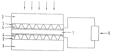
Fig. 1 is a schematic view o a photovoltaic cell containing
current collecting contacts in accordance with
the present invention.
Fig. 2 is a schematic view of current collecting contacts
arranged in the optically transparent polymer block,
where "a" denotPs the sections which are in contact
with the surface of the semiconductor wafer and
~b" denotes the sections which are not in contact
with the surface of the semiconductor wafer.
Fig. 3 is an illustration of various embodiments of a
current collecting contact made of bent wire.
Fig. 4 is an illustration of a çurrent collecting contact
configured as a cylindrical helix.
Fig. S is an illustration of various embodiments of current
collecting contacts made of metal sheet with pro
trusions and depresqions.
Fig. S is an illustration of current collecting contacts
05 configured as a "brush".
Fig. 7 is a schematic plan view of the semiconductor wafer
having current collecting contacts arranged parallelly
to one paix of sides of the semiconductor wafer.
Fiy. 8 is a schematic plan view of a semiconductor wafer
having current collecting contacts arranged parallelly
to the other pair of sides o~ the ~emiconductor
wafer.
Fig. 9 is a schematic plan view of a semiconductor wafer
with current collecting contacts conigured as
a mesh.
Fig. 10 is schematic view of a photovoltaic cell having
conducting strata on the front and the rear ~ide
of the semiconductor wafer.
Fig. 11 is a plan view of a semiconductor wafer and a
dielectric wafer arranged at one edge of the semi-
conductor wafer~
Fig. 12 is a sectional view corresponding to line A-A
in FigO 11.
Fig. 13 is a plan view of a semiconductor wafer and a
dielectric wafer configured as a frame.
Fig. 14 is a cross section corresponding to line A-A in
in Fig. 13.
2~3~
- 12 -
Fig. 15 is a schematic plan view of a dielectric wafer
contacting a semiconductor wafer, with conducting
coatings being applied -to both sides of the dielec-
05 tric wafer at some distance fxom the inner edge of
the wafer.
Fig. 16 is a cross section corresponding to line A-A in
Fig. 15.
Fig. 17 is schematic plan view of a dielectric wafer accor-
ding to Fig. 15 to which conducting coatings have
been applied at some distance from both, the lnner
and the outer edge of the wafer.
Fig. 18 is a cross section corresponding to line A-A in
Fig. 17.
Fig. l9 is an illustration of a battery composed of two
parallelly interconnected photovoltaic cells.
Fig. 20 is an illustration of a battery composed of two
serially interconnected photovoltaic cellsO
5 Fig. 21 is an illustration of various types of serial
interconnection of photovoltaic cells to form
a battery in accordance with the present invention.
DETAILED DESCRIPTION OF THE INVENTION
A photovoltaic cell for converting light energy to electric
energy in accordance with the present invention comprises a
barrier-layer semiconductor wafer 1 and current collec-
ting contacts 2 made of conducting metals or alloys. The
current collecting contacts are configured as electri-
cally connec~ed intermittent ~ections being, respectively,
in (a) and out (b) of contact with semiconductor wafer
1 (Fig. 2). In order to fix the current collecting contacts
they are embedded in an optically transparent polymer
05 block 4 in such a way that at lea~t the sections which
are in contact with the semiconductor wafer surface pro-
trude from the polymer block. From above and from below
the current collecting contacts are compressed b~ opti-
cally transparent protective coatings 3. Glass coatings
or flexible coatings, e.g. Lawsan coatings, are used as
the protective coatings.
Due to the compres6ion forces generated by protective
coatings 3 current collecting contacts 2 are in a state
of tension and, by virtue of their elasticity, remain con-
stantly in contact with the semiconductor wafer surface at
the contact points.
Upon illumination o~ the front side of the photovoltaic
cell, charge separation occurs at the energetic barrier,
and electromotive force i.s generated. As a result, current
flows through current collecting contacts 2 arranqed on
the front side (the side oriented towards incident light)
and on the rear side (the shadowed side) of semiconductor
wafer 1, which leads to power generation on load resistor
5. Contact resistance at the points of contact between
current collecting contacts 2 and semiconductor wafer
1 is rather low due to the compression forces generated
by protective coatings 3 and because of the elasticity
of the current collecting contacts themselves.
In the photovoltaic cell in accordance with the present
invention, 10 percent or less of the projection area of
current collecting contacts 2 on the surface of wafer 1 is
in direct contact with photosensitive semiconductor wafer 1.
~ 3,~ 2
This means that the remainin~ 90 percent of the wire pro~ec-
tion area is also illuminated, though not by perpendicular
light beams. This additional illumination oE the surface oE
photosensitive semiconductor wafer 1 leads to a higher
05 conversion efEiciency of the photovoltaic cell as a whole.
The configuration of current collecting contacts 2 as
claimed herein allows to significantly simplify their
fabrication as the step of embedding current collecting
elements 2 in optically transparent pol~mer block 4 is
performed separately~ and polymer blocks 4 with contacts
2 embedded therein are then used in the step of assembling
photovoltaic cells and interconnecting them to form batteries.
Contact between current collecting contacts 2 and the surface
of semiconductor wafer 1 as well as interconnection and
sealing of the photovoltaic cell are provided in one single
step by heating the assembled cell up to a temperature of
about 100 to 120C and applying external pressure of up
to 1 atm.
Current collecting contacts 2 may be made of conducting
bent wire. The wire may be bent periodically or aperiodi-
cally in the form of a sinu~oid, a triangle, a trapeze,
a rectangle, or a Elat helix, as well as various combin-
nations of these geometric figures (Fig. 3). The wire
bending may be completely arbitrary.
The current collecting contacts may also be configured
as a bus having wire sections attached thereto, with the
lower free ends of said wire sections contacting the sur-
face of the semiconductor waEer (in the form a "brush")
(Fig. 6a and 6c). The brush pitch is of no importance
whatsoever.
~5
- 15 -
Wire sections may also be arranged on both side3 of one
common bus (Fig. 6b).
Furthermore, the current collecting contacts may be con-
05 figured as a cylindrical helix (Fig. 4) or made of a metal
sheet with protrusions and depre~sions tFig. 5). The position
of these protrusions and depressions relative to each okher
as well as their shape are of no par~icular importance.
What is important is that due to the state of tension and
the elasticity of current collecting contacts 2 a reliable
contact be provided between these contacts and the surface
of semiconductor wafer 1.
In the photovoltaic cell, current collecting contacts
2 arranged on each of the two sides of semiconductor wa-
fer 1 may either be of the same type, e.g. configured
as bent wire, or represent various combinations of contacts
2, such as bent wire - cylindrical helix - comb - brush.
Current collecting contacts 2 may be arranged either co-
axially to the longitudinal axis of semiconductor wafer
1 (Fig. 7) or perpendicularly thereto (Fig 8), i.e.,
parallelly to one pair of sides of the semiconductor wa-
fer, as well as, for example, be arranged coaxially or
perpendisularly to the longitudinal axis of the semi-
condu~tor wafer on the front side, and reversely on the
rear side, i.e. parallelly to different pairs of sides of
the semiconductor wafer. In addition, the current collec-
ting element may be configured as a mesh. This mesh may
comprise various current collecting contacts, such as wires,
helixes, planar elements, "brushes", etc. An exampla of
a mesh design composed of bent and straight wires is shown
in Fig. 9. The wires optionally ma~ be fixed to each other
at the crossing points. If they are connect~d at the
at the crossing points. If they are fixed at the crossing
2 ~
- 16 -
points, this leads to enhanced mechanical strength, lower
series resistance and a sir.lplified assembl~ technique.
Contact resistance at the points of contact between current
05 collecting contacts 2 and the surface of semiconductor
wafer l is significantly reduced, if at least the front
surface of the semiconductor wafer is coated with an anti-
reflectlve conducting coating 6 (Fig. 10) characterized
by a high concentration of charge carriers (more than
102/cm~3). This antireflective conducting coating
may be selected from known materials which are commonly
used in constructions of photovoltaic cells. If illumina-
tion of the rear side of the photovoltaic cell is possib-
le, it is adviseable to apply the antireflective coating
to both sides of the semiconductor wafer, as this enhances
the efficiency of the photovoltaic cell.
In constructions of photovoltaic cells where only the
front surface of semiconduc-tor wafer l is exposed to in-
cident light energy, it is recommendahle to provide onthe rear side of semiconductor wafer 1 a highly-doped
near-surface layer having the same type of conductivity
as semiconductor wafer l, or to deposit a metal layer,
to provide for low contact resistance between the current
collectins contact and the semiconductor wafer. This will
lead to lower contact resistance and higher open~circu.it
voltage of the photovoltaic cell and, consequently, to
enhanced efficiency.
The proposed construction of current collecting contacts
2 makes it possible to significantly simplify the inter-
connection of contacts and to eliminate the time-consllming
soldering process which is difficult to automateO To facili-
tate interconnection of contacts, a dielectric wafer 8 i~
provided in the photovoltaic cell (FigO ll - 14)~ said wafer
2~3~8~
being arranged coplanarly with semiconductor wafer 1 and
at least at one edge of the latter. Dielectric waer 8 is
coated on both sides with a layer of conducking material
lO to which current tapping electrodes 9 are connected, e.
05 g., by soldering. Dielectric wafer 8 is arranged to form an
air gap ll relative to semiconduc~or 1. A dielectric spacer
element 12 may be arran~ed between dielectric wafer 8 and
semiconductor wafer 1 (Fig. 14). To prevent electric contact
between conducting coating 10 of dielectric wafer 8 and semi-
conductor wafer l, the conducting coating 10 may be appliedto dielectric wafer 8 at some distance from the edge
(Fig. ll - 18)o
Current collecting contacts 2 arranged on the front side
and the rear side of semiconductor wafer 1 are applied,
respectively, to each of the two sides of dielectric wafer 8,
and pressed against conducting material 10 due to the
compression force generated by protective coatings 3 and
their own elasticity. The photovoltaic cell i~ connected
to load resistor 5 via current tapping electrodes 9. Since
the thickness of the dielectric wafer preferably is equal
to or somewhat greater than the thickness of the semiconduc-
tor wafer, current collecting contacts 2, due to their
elasticity, maintain constant contact with conducting coating
10 of dielectric wafer 8. Rather low contact resi~tance
between current collecting contacts 2 and conducting coating
lO is provided in result of using a material having a high
concentration of charge carriers (more than 102/cm~3)
and low sheet resistance (less than lO~lohm/ ), e.g. a
metal, as the conducting coating. If one dielectric wafer
8 is used, current collecting contacts 2 are interconnected
via a bus on the opposite edge or, if a mesh is used, on the
other three edges of the dielectric wafer.
A preferred embodiment o~ the interconnection element
~ ~ S~ 8 ~
- lB -
(Fi.g. 13, 14) iS a dielec~ric frame 8 wlthin which semi-
conductor wafer 1 is arranged, which is separated from
said frame by an air gap 11 or a dlelectric spacer element
12. In that case, dielectric frame 8 is also covered on
05 both sides with conducting coating 10 to which current
collecting contacts 2 are applied. Here, too, as described
above, it is possible that the dielectric wafer i8 not
completely covered with conducting coating 10 (Fig. 15 -
18). This construction, which has all the ad~anta~es men-
tioned above for the above described construction wheraa dielectric wafer is arranged at one edge of the semi-
conductor wafer, makes it possible to completely abandon
the soldering process and automate the fabrication of
both, individual photovoltaic elements and batteries
assembled therefrom. This is accomplished by forming a
number of openinqs in a dielectric wafer 8 covered on
both sides with conducting coatings, in which openings
semiconductor wafers 1 covered with antireflective coa-
ting 6 and conducting coating 7 are inserted. The pre-
fabricated ribbons of optically transparent polymer ma-
terial 4 with current collecting contacts 2 embedded
therein are applied from above and from below to semi-
conductor wafer 1. Polymer ribbons 4 can be made of opti-
cally transparent adhesive sealant material or may be
coated from above and from below with a layer of such
material. From above, protective coatin~s 3 are applied
to polymer material 4, which protective coatings are either
of glass or, for example, of Lawsan, which provides for
a flexible protective coatin~.
Upon assembly, the wllole construction of the photovoltaic
cell. is lleated up to t:he flow temperature of the poly
mer tabout 100 - 120C). Due to the application of ex-
ternal pressure (up to 1 atm) the polymer flows from the
~ones whera semiconductor wafer 1 and dielectric wafer
~ ~3 ~ X ~
-- 19 --
2 are located into the gap between them or in any techno~
logical gaps between them. Since temperature and pres~ure
are relatively low, semiconductor waer 1 and dielectric
wafer 8 do not move apart from each other. During heating
OS and compression protective coating 3 and semiconductor
wafer 1 are adhesively bond~d to the adhesive sealant
polymer which has been applied to polymer block 4 or of which
polymer block 4 is made.
Photovoltaic cells in accordance with the present invention
are employed for assembling batteries.
Any type of interconnection, both serial and parallel,
can easily be provided.
ParalIel interconnection of two photovoltaic cells i~
schematically shown in Fi~. l9o In that ca~e, current
collecting contacts 2 arranged on the front side of ~emi-
conductor wafer l of the first photovoltaic cell are elec-
trically connected to current collecting contacts 2 arrangedon the front side of semiconductor wafer 1 of the other
photovoltaic cell, and the current collecting contacts
arranged on the rear side of the two semiconductor wafers
are connected correspondin~lyO The free ends of current
collecting contacts 2 of both photovoltaic cells are connec-
ted to the corresponding current tapping electrodes 9.
In the case of serial interconnection (Fig. 20) of photo~ol-
taic cells, current collecting contacts 2 arranged on the
rear side of semiconductor wafer l of the firsk photovoltaic
cell are electrically connected to current collecting
contacts 2 arran~ed on the front side of semiconductor wafer
1 of the adjacent photovoltaic cell, and the current collec-
ting contacts 2 arranged on the front side of semiconduc-
tor wafer l of the fir.st photovoltaic cell and the current
r~ ~3 8 ~
- 20 -
collecting contacts 2 arranged on the rear side of semicon-
ductor wafer 1 of the second photovoltaic cell are connected
to the corresponding current tapping electrodes 9. This
connection is schematically shown in Fig. 20.
05
In order to reduce resistivity of current collecting con-
tacts 2 a metallic conductor 15 may be provided in the
constructions according to Fig. 7, 8, 11, 12, 19 and 20,
which conductor may be configured as a wire or a metalli-
zed dielectric of any shape, which electrically contactscurrent collecting contacts 2. This conductor 15 may be
arranged either in the surface area or near the edyes of
silicon wafer 1 and may electrically contact metallized
dielectric frame 8. In the embodiment according to Fig.
lS 11 and 12, two conductors lS are fixed to each other at
the crossing point, and one o~ the conductors 15 is conn~c-
ted to metallized dielectric wafer B.
Possible varieties of serial interconnection of photovoltaic
cells to form a battery are shown in Fig. 21 (a, b, c, d).
In the embodiment according to Fig. 21a, serial interconnec-
tion of photovoltaic cells is accomplished by providing
a system o~ cuttings, holes and jumpers 13 in dielectric
wafers 8 covered by metallized coating 10, by means of which
system the metalliæed coatings are interconnected.
A continllous metal wafer 14 can be used instead of the
dielectric wafer, by means of which the front side and
the rear side of two serially interconnected photovoltaic
cells are connected (Fig. 21b).
Fig. 21c shows a battery composed of photovoltaic cells,
wherein the basic semiconductors have various types of
conductivity.
2 1~
- 21 -
Fig. 21d shows a hattery assembled from serially inter-
connected photovoltaic cells having the same type o~ conduc-
tivity and such a rear sid~ sensitivity that upon illumina-
tion of the rear side, the efficiency of this photovoltaic
05 cell differs little from its efficiency in the case of illu-
mination of the front side.
In the case of parallel interconnection as well as in
the case of serial interconnection of photovoltaic cell~
to form a battery, the contact systems of the photovoltaic
cells can be hrought out and interconnected. Construc-
tions of photovoltaic cells in accordance with the present
invention have been realized using various materials and
tested in comparison with photovoltaic cells fabricated
using known techniques.
Tests have shown that a photovoltaic cell in accordance
with the present invention, when illuminated at 1000 W~m2,
has an efficiency of 16 to lS percent as compared to known
photovoltaic cells, which have an efficiency of 12 percent.
Photovoltaic cells in accordance with the invention were
operated for 60 days at a temperature of 80C without
any chan~e in efficiency, which corresponds to 10 years of
operation at room temperature.