Note: Descriptions are shown in the official language in which they were submitted.
2036~28
ELECTRIC DOUBLE LAYER CAPACITOR
BACKGROUND OF THE INVENTION
The present invention relates to an electric double
layer capacitor of high electrostatic capacitance which
utilizes the princlples of an electric double layer that is
composed of an interface between activated carbon and
electrolyte.
Recently, high-capacitance capacitors based on the
electric double layer principles have been developed as
backup power supplies for memories in electronic systems,
and are wldely used with microcomputers and IC memories.
one type of electric double layer capacitor is dis-
closed ln U.S. Patent 3,536,936, for example. Disclosed
electrlc double layer capacltor comprlses a frame-shaped
gasket, a palr of polarlzed electrodes made of activated
carbon partlcles and dlsposed ln the gasket, a separator
dlsposed between the polarlzed electrodes for preventlng
electrons from movlng between the electrodes, and a palr of
current collectors mounted respectlvely on the opposite sur-
faces of the polarlzed electrodes and havlng perlpheral
edges bonded to the gasket. The polarized electrodes are
made as paste electrodes from a concentrated slurry whlch ls
a mixture of powdery or partlculate actlvated carbon and an
electrolyte.
It ls lmportant that the lnternal resistance of
such an electrlc double layer capacltor wlth paste elec-
- 1 - ~
; ' '.. " : '' ,' ' '"' :
,.
. .
.
- 2036028
trodes be low. The internal resistance of an electric dou-
ble layer capacitor is greatly affected by the contact
resistance of active carbon of the polarized electrodes and
the contact resistance between the collector electrodes and
the polarized electrodes.
Therefore, in order to reduce the internal resis-
tance of the polarized electrodes and the contact resistance
between the collector and polarized electrodes, each basic
cell of the electric double layer capacitor should be kept
under vertical pressure to bring the particles of the paste
activated carbon into good electric contact with each other.
Conventlonal electric double layer capacitors require each
cell to be kept under a pressure of about lOo kg/cm~ though
lt depends on the size of the electrodes, the size of the
partlcles of the carbon material, or the kind of the elec-
trolyte used. In prlor electrlc double layer capacltors,
the cells are kept under pressure by deforming the outer
cases of the capacltors or bondlng the current collectors
strongly to gaskets. If an electrlc double layer capacltor
ls to be used as a large-capacitance capacitor, e.g., a
power supply for energlzlng a motor, then lt is necessary to
lncrease the cross-sectlonal areas of the electrodes of the
basic cell. Therefore, the pressure to be applied to the
baslc cell has to be lncreased. Increaslng the pressure,
however, causes some practlcal problems such as the selec-
tion of means for applying the pressure and the need for
.. . .....
2036028
high rigidity for the outer cell which houses the basic
cell.
The contact resistance between the polarized elec-
trodes and the current collectors of conventional electric
double layer capacitors is so large that it is responsible
for presenting a high internal resistance. One proposed
electric double layer capacitor which has a reduced contact
resistance between the polarlzed electrodes and the current
collectors and hence a reduced internal resistance is dis-
closed in Japanese Laid-Open Patent Publication No.
63(1988)-232309.
According to the disclosure of the above
publicatlon, a thermoplastic resin is heated and dissolved
in an electrolytic solution, and the solution is cooled into
a gel which does not flow or is not deformed and remains in
a solld phase unless an external force is applied thereto.
Then, powder of activated carbon is added to the gel, and
the mlxture ls kneaded by a roll mill. The kneaded mlxture
ls shaped lnto a sheet which is cut off into polarized
electrodes. Metallic powder of stainless steel is sprinkled
over one surface of each of the polarlzed electrodes, and
the sprlnkled powder partlcles are embedded in the surface
of the polarlzed electrode by belng pressed by a roll, thus
provldlng an electrlcally conductlve layer whlch wlll reduce
the contact reslstance between the polarlzed electrode and a
current collector. Since the electrically conductive layer
' ' " '' . :
:
.
2~36~28
.
is formed after the polarized electrode is fabricated,
however, an increased number of processing steps are
required to manufacture the electric double layer capacitor.
In addition, the contact resistance between the polarized
electrode and the electrically conductive layer is not sat-
isfactory enough since they are electrically coupled to each
other through contact between the particles.
SUMMARY OF THE INVENTION
It is an ob~ect of the present invention to provide
an electric double layer capacitor which utilizes the prin-
clples of an electric double layer that is composed of an
lnterface between actlvated carbon and electrolyte, the
electrlc double layer capacitor havlng an electrically con-
ductlve layer on a surface of an electrode body to reduce
the contact reslstance between the electrode body and a cur-
rent collector, and the electrode body and the electrlcally
conductlve layer havlng a reduced contact reslstance the-
rebetween so that the capacitor has a reduced lnternal
reslstance.
Another ob~ect of the present invention is to pro-
vlde a method of manufacturlng an electrode for an electric
double layer capacltor, the method belng capable of reliably
forming an electrically conductlve layer on a surface of an
electrode body.
Accordlng to the present lnvention, there is pro-
vlded an electric double laye~ capacitor having an electric
203~28
double layer composed of an interface between activated car-
bon and electrolyte, comprising a pair of electrode bodies
having surfaces confronting each other, each of the elec-
trode bodies comprising a porous sintered body of joined
active carbon particles, a pair of electrically conductive
layers formed on respective other surfaces of the electrode
bodies at the time the electrode bodies are sintered, a sep-
arator interposed between the electrode bodies, a gasket
housing the electrode bodies and the separator therein, and
a pair of current collectors disposed on the respective
other surfaces of the electrode bodies in contact with the
electrically conductive layers, respectively, the current
collectors having respective peripheral edges joined to the
gasket.
According to the present invention, there is also
provlded a method of manufacturing a polarized electrode for
an electric double layer capacitor havlng an electric double
layer composed of an interface between activated carbon and
electrolyte, the method comprising the steps of placing an
electrlcally conductlve materlal in a sintering mold, plac-
ing powder of mlnute active carbon partlcles on the electri-
cally conductlve materlal ln the slnterlng mold, presslng
the powder of mlnute active carbon particles and the elec-
trlcally conductlve materlal ln the slntering mold, and
slnterlng the powder of mlnute actlve carbon particles and
the electrically conductlve material while under pressure,
-- 5 --
' ~, ", : :,
. . .
. . ..
203~028
thereby forming an electrically conductive layer and an
electrode body, respectively, which are intimately joined to
each other.
The above and other ob;ects, features and advan-
tages of the present invention will become more apparent
from the following description when taken in con~unction
with the accompanying drawings in which a preferred embodi-
ments of the present invention is shown by way of illustra-
tive example.
BRIEF DESCRIPTION OF THE DRAWINGS
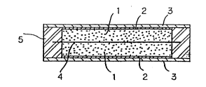
Fig. 1 is a cross-sectional view of an electric
double layer capacitor according to the present invention;
Fig. 2 is a cross-sectional view of an electrode
servlng as a polarlzed electrode ln the electric double
layer capacltor;
Flg. 3 ls a circuit diagram showlng an apparatus
for manufacturlng a porous slntered body as an electrode
body accordlng to the present lnvention;
Flg. 4 is a graph showing the pressure applied to
mlnute active carbon partlcles, the average current flowing
through the minute active carbon particles, and the tempera-
ture of the minute active carbon particles, as they change
with tlme; and
Fig. 5 ls a table of electrostatlc capacltances and
lnternal reslstances of electric double layer capacitors
according to lnventlve and comparatlve examples.
2036028
DETAILED DESCRIPTION OF THE PREFERRED EMBODIMENT
Fig. l shows in cross section an electric double
layer capacitor according to the present invention.
The electric double layer capacitor comprises a
palr of polarized electrodes l with surfaces confronting
each other. Each of the polarized electrodes 1 can be manu-
factured by a sintering apparatus as shown in Fig. 3.
Speclfically, powder of minute active carbon particles hav-
lng an average particle diameter of about 20 ~m is sintered
into a porous sintered electrode body, which is then impre-
gnated with dllute sulfuric acid.
The electric double layer capacitor also includes a
pair of electrically conductive layers 2 which are formed
respectlvely on the other surfaces of the electrode bodies
of the polarlzed electrodes 1 at the tlme the electrode bod-
ies are slntered. Each of the electrlcally conductive lay-
ers 2 1B made of metallic powder or foll that is lntegrally
~olned to the electrode bodies in a manner as described
later on.
The polarized electrodes 1 are housed ln an annular
gasket 5 which ls made of electrlcally nonconductive rubber
or synthetic resLn. The polarized electrodes 1 are sepa-
rated from each other by a separator 4 dlsposed
therebetween. The separator 4 may in the form of a piece of
nonwoven fabrlc of porous polypropylene whlch ls lmpregnated
wlth an electrolytlc solutlon. The separator 4 allows ions
,, .
, . ~ , , .
.. .. .
, - , .
. .
2036~28
to pass therethrough, but prevents electrons from moving
therethrough. The electric double layer capacitor further
includes a pair of current collectors 3 disposed respec-
tively on the outer surfaces of the electrically conductlve
layers 2 on the polarized electrodes 1. Each of the current
collectors 3 is made of an electrically conductive film
which is produced by kneading powder of electrically conduc-
tive material and synthetic resin. The current collectors 3
have peripheral edges bonded to the gasket 5.
A method of manufacturing each of the polarized
electrodes 1 with the electrically conductive layer 2, as
shown in Fig. 2, will be described below with reference to
the slnterlng apparatus shown ln Flg. 3.
As shown in Fig. 3, powder of minute active carbon
partlcles ls placed ln a slntering mold 10. The sintering
mold 10 ls made of a hlghly strong metal such as tungsten
steel, and has a central hole for placing active carbon par-
ticles therein. The lnner wall of the hole ls coated wlth
an lnsulatlng layer 11 whlch ls made of an lnsulating mate-
rlal such as sllicon oxlde (Sl02) or slllcon nltride (Si~N~)
and deposited by a known process such as vapor growth.
Upper and lower plungers 12, 13 have lower and upper ends,
respectlvely, lnserted in the hole ln the sinterlng mold 10.
The upper and lower plungers 12, 13 are made of a heat-
reslstant metal such as tungsten, molybdenum, or the like.
The upper and lower plungers 12, 13 are connected respec-
tively to upper and lower electrodes 14, 15.
2036028
Although not shown in Flg. 3, the upper and lower
plungers 12, 13 and the upper and lower electrodes 14, 15
are controllably pressed by a hydraulic press in the direc-
tions indicated by the arrows F so that a desired pressure
can be imposed on minute particles for forming the polarized
electrode 1 and an electrically conductive material for
forming the electrically conductive layer 2, which are
placed in the sintering mold 10. The minute particles and
the electrically conductive material which are contained in
the sintering mold 10 are placed in a desired atmosphere.
The upper and lower electrodes 14, 15 are electrically con-
nected to a series-connected circuit of switches SWl, SW2
and a capacitor C, and a series-connected circuit of a vari-
able resistor R and a variable-voltage power supply 16 is
connected parallel to a serles-connected circuit of the
capacltor C and the switch SW2. The on- and off-times of
the swltches SWl, SW2 are controlled by a switch control
circult 17. The swltch SWl comprlses a normally open
swltch, and the swltch SW2 comprlses a normally closed
switch.
The slnterlng mold l0 may be made of a ceramic
materlal such as slllcon oxlde (S10,), slllcon nitrlde
(Sl,N~), slllcon carbide ~SlC), or the like.
Operation of the apparatus shown in Flg. 3 for the
manufacture of an electrode body whlch wlll form a polarlzed
electrode of an electrlc double layer according to a flrst
lnventive example will be descrlbed below.
2036~28
With only the lower plunger 13 inserted in the hole
in the sintering mold lO, stainless steel powder having an
average diameter of about 5 ~m, which will form an electri-
cally conductive layer 2, is placed on the lower plunger 13
up to a thickness ranging from 50 to 100 ~m. The upper
plunger 12 is then inserted into the hole in the sintering
mold 10 to press the deposited stainless steel powder.
Thereafter, the upper plunger 14 is lifted out of the hole
in the slntering mold 10. Then, over the compacted stain-
less steel powder, there is placed powder of minute active
carbon particles having an average diameter of about 20 ~m
until the deposited powder has a thickness of 1.5 mm. The
upper plunger 12 is again inserted into the hole in the
slnterlng apparatus 10 to press the deposited powder of min-
ute actlve carbon particles and the stainless steel powder
under a predetermined pressure. Then, whlle the compacted
powder of minute actlve carbon partlcles and stalnless steel
powder are belng pressed, the switch SWl is controlled so
as to be repeatedly turned on and off.
The on-time of the switch SWl ls controlled so that
it i8 egual to or shorter than a dlscharge time in whlch the
charges ln the capacitor C are discharged between the upper
and lower electrodes 14, 15. The off-tlme of the switch SWl
i8 controlled so that it is substantially equal to or longer
than a charge tlme ln whlch the capacltor C can be charged.
Therefore, a current flowlng between the upper and lower
-- 10 --
2036~2~
electrodes 14, 15 is rendered variable from a maximum value
to a minimum value.
When the switch SWl is thus repeatedly turned on
and off, sharp pulsed impulse currents flow between the
upper and lower plungers 12, 13, as shown in Fig. 4.
The pulsed impulse current is supplied between the
upper and lower plungers 12, 13 untll almost all the minute
particles of active carbon sandwiched between the upper and
lower plungers are brought into contact and fused to each
other. Thereafter, while the pressure applied to the minute
particles is being kept at a constant level, the switch Sw2
ls continuously turned off and the swltch SWl ls continu-
ously turned on, and the resistance of the variable resistor
R and the voltage of the variable-voltage power supply 16
are regulated to contlnuously pass a heating current of a
glven value between the upper and lower electrodes 14, 15,
as shown ln Flg. 4.
After a target temperature ls reached, the heating
current whlch ls supplied is kept at a constant level for
thereby maintalning the porous sintered body of active car-
bon whose temperature has been increased thus far at a con-
stant temperature (see Fig. 4).
Under such a condltion, the mlnute active carbon
partlcles of the porous sintered body are stably bonded
together, and the stainless steel particles for formlng an
electrlcally conductive layer on one surface of the porous
-- 11 --
- . . : .
203~0~8
sintered body enter the interstices of the porous sintered
body and are held in intimate contact therewith. Now, the
discharge voltage applied between the upper and lower elec-
trodes i4, 15 is turned off, and the pressure applied ther-
ebetween is also cut off. When the temperature of the
porous sintered body has dropped to normal temperature, the
porous sintered body ls removed from the sintering mold lO.
As shown in Fig. 2, the electrode body, denoted at
la, thus fabricated supports on its one surface an electri-
cally conductive layer 2 of sintered stainless steel powder.
Two such electrode bodies are combined together, and impr-
egnated with dilute sulfuric acid. Using the polarized
electrodes 1 thus fabricated, an electric double layer
capacltor constructed as shown in Fig. 1 is manufactured.
An electric double layer capacitor according to a
second inventlve example is manufactured as follows:
Except that copper powder ls employed instead of
the stainless steel powder in the first inventive example,
the same materlals as those ln the flrst inventive example
are used, and an electrode body ls fabricated using the
slnterlng apparatus shown in Flg. 3 in the same manner as
the flrst lnventlve example.
An electrlc double layer capacltor according to a
thlrd lnventlve example ls essentlally the same as the first
inventive example except that gold powder ls employed
lnstead of the stainless steel powder ln the flrst inventlve
example.
- 12 -
, , ,
. ., ~ . .
- , , .", .
.. . ..
,
.. ; - ~ ,,,
- 2~3~
An electric double layer capacitor according to a
fourth inventive example is essentially the same as the
first inventive example except that stainless steel foil is
employed instead of the stainless steel powder in the first
inventive example.
Fig. 5 shows a table of electrostatic capacitances
and lnternal resistances of the electrlc double layer capac-
itors according to the first through fourth inventive
examples and also an electric double layer according to a
comparative example. The electric double layer capacitor
according to the comparative example includes a pair of
polarized electrodes each comprising an electrode body com-
posed of a sintered body of active carbon power having an
average particle diameter of 20 ~m and coated with acetylene
black. In each of the inventive and comparative examples,
the electrode body has a diameter of 20 mm.
Study of Fig. 5 indlcates that the electrostatic
capacltances of the electric double layer capacltors of the
lnventlve and comparative examples are substantially the
same. ~owever, the lnternal reslstances of the,electrlc
double layer capacltors accordlng of the first through
fourth examples are l/4, 2/15, l/lO, and 1/15, respectively,
of the lnternal reslstance of the electrlc double layer
accordlng to the comparatlve example, for the reason that
the electrode body ls held ln contact with the current col-
lector through the electrlcally conductlve layer which is
held in lntlmate contact with the electrode body.
- 13 -
- , ..
,, ~, . . . .
2036~28
With the present invention, as described above, an
electrode body, which will be impregnated with an electro-
lytic solution to form a polarized electrode, is held in
contact with a current collector through an electrically
conductive layer which is made of metal powder or foil and
lntimately ~oined to the electrode body at the time the
electrode body is sintered. Therefore, the electrically
conductive layer is held in intimate contact with a rough-
ened porous surface of the sintered electrode body. The
electric resistance between the electrode body and the cur-
rent collector through the electrically conductive layer is
thus reduced, so that the electric double layer capacitor
has a reduced internal resistance.
As described above, the electrically conductive
layer is formed on the electrode body at the same time that
the electrode body is sintered by the sintering mold.
Therefore, no special dedicated device is needed to form the
electrically conductive layer on the electrode body.
Consequently, the electric double layer capacitor of good
performance can be manufactured according to a simple man-
ufacturlng process.
Although a certain preferred embodiment has been
shown and described, it should be understood that many
changes and modifications may be made thereln wlthout
departlng from the scope of the appended clalms.
- 14 -
. . .
'
.. ~' : '
. - , - ' '" , . '