Note: Descriptions are shown in the official language in which they were submitted.
203~17~
CONTRO~ NAI ~;pRF~nFR
RACK(;~OUNn OF THF INVFNTION
The present invention relates to a system for smoothing or spreading
transitions between regions of an image transmitted by a television sign~ which
are processed in a first way and those which are processed in a seccnd
different way.
Processing of standard television sign~s, (such as NTSC or PAL), which
represent images, is often chansed to adapt to the environment of the signal.
This adaptive processing can result in some regions of an image being
processed in one way and other adjoining regions being processed in a
different way. If the processing differences can be perceived by a viewer, the
different regions, and the transition between them, can be discerned, and image
quality is degraded.
For example, when separating chrominance and luminance components
from the composite video signal, a frame comb filter may be used. As long as
there is no change in the image over a frame time interval, the iuminancs and
chrominance components can be completely separated. If the scene changes
over the frame time interval, then some color inforrnation will be present in the
separated luminance component and some brightness information will be
present in the chrominanca co""~onertt.
A line comb filter will also separate the luminance and chrominance
components from the co",posite video signal and does not produce significantly
degraded component signais in the presenc~ ot image motion. I lovJever, a line
comb fllter red~ces the vo.llcal resolution ot the r~p~duced image relative to a
- 2036175 -
frame comb filter. In addition. in locations whQre a vertical transition occurs, an
image processed by a line comb fiiter may be degraded due to color information
being introduced into the luminance component, producing an image artifact
known as hanging dots; and brightness information being introduced into th~
chrominance, producing incorrect colors in the neighborhood of the transition.
The television signal may be adaptively processed by detecting the
presence or absence of image motion. In regions in which the image is
stationary, the frame comb filter is used, and in resions in which the image is
chansing, the line comb filter is used.
Another example of such adaptive processing is an adaptive double-
scanned non-interlaced scan converter. In such a converter, interstitial lines are
displayed between lines of the current field. The interstitial lines may be those
from the preceding held, however, in such presence of im~ge changes, visible
artifacts, such as serrated edges, occur. The interstitial lines may aiso be
interpolated from lines within the current field, but the vertical resolution isreduced and line flicker may occur. In regions in which image changes are
detected, intrafield interpolated interstitial lines are displayed and held~elayed
interstitial lines are displayed othenNise.
Yet another example is an adaptive peaking circuitry in which regions
having relatively high noise are processed with a relatively low peaking factor
and regions having relatively low noise ars processsd with a relatively high
peaking factor.
In all of the above exa-"ples, the pro~ssing of the television signais`is
changed in response to the value ot an estimated parameter of the imags. The
parameter is motion in the case ot luminance/chrominanca separation and
double scanning non-interlaced conversion, and it Is the relative level of noisein the case ot the peaking. Dlfferently processsd regions, and noticeable
203617~
boundaries between those regions where the parameter is present and where it
is absent is an undesirable artifact introduced by the above types of adaptive
proc~ssing. It is desirable to reduc~ the visibility of this artifact in such systems
and thereby improv~ the perceived quality of the image.
In accordanc2 with the invention described in U.S. Pat No 4,B68,6~0,
issued en Sept. 19, 1989, to H. J. Wec~enbroc~, a parameter of the composite
video signai is estimated for points in the image. A control signal is then
generated based on the parameter. This control signal may be used to control
the selection of processing modes. The value of the control signal is then
spread symmetncally in a gradually decreasing manner around the region in
which the control signal is generated in at least one direction. This generates a
region in which the procossing gradually changes from a region in which one
type of processing is performed to that in which the other type of processing isperformed.
RRIFF SUMMAFIY OF THF INVFNTION
In the following description of apparatus for spreading a control signal,
the word ~horizontal~ will refer to a direction along the scan lines and the word
~vertic~ will refer to a direction perpendicular to the scan lines. Although theinventicn can be carried out by analog circuits, it will be described in digitalforrn.
As the control siy"als are derived for pixels along the scan lines, they
have a fixed control signal amplitude such as one, and the rest of the signals
have reference values such as zero. As is well undelstood by those sl(illed in
the art, each scan line has a fixed number ot pixels, and when this number ot
- 20~61~5
plxels is received, image forming apparatus places the next pixel at the
beginning of the next line.
In accordanc~ with this invention, the control signal is applied to a
horizontal widener ~nd a vertical widener that ar~ connected in series in eitherorder. Th~ honzontat widener repeats each logic 1 of a control signal n times,
where n is equal to the number of clock delay elements in the horizontal
widener 32, and the vertical widener repeats each scan line m times where m
is equal to the number of line delays, denoted by ~1-H~ delays, in the vertical
widener 34. Thus m +1 identical scan lines are produced, each having 1's at
the locations along the lines where the originai control signals occurred and n
more 1's occurring immediately thereafter.
As the extended set of control sisnal values, including the repeated scan
lines, emerges from the horizontal and vertical wideners, it is applied to a line
signal spreader that creates a ramp of increasing values starting at the first
onginal control signal pixel and extending throush the 1 pixels following it. The
line signal spreader retains the maximum value it created at the end of the rampof n pixels until the last 1 has been recsived. At this point, the line signal
spreader creates a ramp of decreasing values during the following r pixels, it
being understood that r may be equal to n to achieve symmetry between th~
ramp of increasing values and the ramp of decreasing vatues.
Thus instead of having a controi signal that abruptly changes from a O to
a 1 and back to a 0, the line signat spreader generates a signal that gradually
changes from a O to a ma~dmum vatue, such as 7, at the point where the originat
control signat just appeared, retains this value during a number of clock cyctesequal to the number of contiguous control signats and then graduatly decreases
that signal bacJc to a Yatue of 0. At this pcint there are m+1 identicat lines.
2036175
Whereas this spreads the control si~nal honzontally along ~ach of m 11
lines there is no vertical spreading because all the lines have the same values.Vertical spreading is achieved in accordanc~ with the preferred form of this
invention by effectively forming a window that is one c!oct< cyc~e wide and m+1
lines high. This window is scanned horizontally until the end of the lines are
reached and then dropped by one line before again scanning across the lines.
The control signal value for the point corresponding to the bottom of the windowis a function of all the values within ths window. Simple addition of the valueswithin this window has been found to work well.
As is weil understood by those skilled in the art the necsssary delays
required to obtain the spread control signals in this manner will cause the
spread control values for the original control signals to be delayed by n pixel
inten~als plus m scan line intervals with respect to the corresponding video
signal. This can be corrected by delaying the video signals by n pixels and m
line scanning intervals.
A distinc~ advantage of this method for spreading control signals is that
the maximum value of the rising ramp occ~rs at the first onsinal control signal
pixel and not at some later pixel as in other methods.
RF~IF~ nF~ lPTl-~N OF THF nRAWlN~
hg. 1 is a block diagram of television equi~.",6"l in which a control signal
representing motion is spread so as to create a better color image from siyllalstransmitted in accG-~nce with the NTSC sla~ d.
Fig. 2 is a bloclc diagram of a control sisnal spreader constructsd in
accordance with this inventlon.
Fig. 3 ill~ as the circuits of one e.l~ t of this inve.,llG,).
2036175
Figs. ~A through 3E respectively represent signal vaiues appeanng at
correspondingly lettered polnts in Fig. 3.
Fig. 3B~ illustratss operation when the position of the horizontal and
vertical wideners are reversed.
Fig. 4A throush 4E respectively represent signal values proaucad at like
lettered points in Fig. 3 as they would be computed to derive the final contro~
signal values as shown in Fig. 4E.
Fig. 5 illustrates a line signal spreader usins PROMs r~ther tha" M'JXes
as in Fig. 3.
Fig. 5A is a table explaining switching functions of Fig. 5.
nFTAII Fn DFSCRIPTION
The illustrated embodiment described below will be disc! ~ssed ,n terms of
a motion adaptive luminance/chrominanca separator. A simiiar arrangement
could be used for other adaptive processing circuits such as double scanned
noninterlaced adaptive scan conversion, or adaptive peaking.
In Fig.1 a composite video signal such as that derived from an NTSC
telecast by a television receiver is applied at terminal 10. A motion detec.or 12
provides a signal having a value such as 1 when motion is considered to exist
and a reference signal 0 when motion is not considered to exist to a signal A-
spreader t4 such as described herein. A 'k' value generator 16 responds to the
signal at the output of the signal spreader 14 to produce values of k and 1-k for
the control ot soft switches 18 and 20. The coi"~osile video signal at terminal
10 is applied via a matching delay 22 to a frame comb 24 and via a matching
delay 26 to a line comb 28.
- 2036175
When there is no motion in the image, the output of the fram~ comb 24 is
used to provide the luminance signal YFC and the chrominanc~ signal CFc
Frame comb filters take advantage of the fact that in the absence of motion two
composite video images separated by a framQ time interval differ only in the
phase of the chrominance signal. Therefore, when two composite video signals
one frame apart are added. the chrominance is cancelled whereas the
luminance is reinforced, so as to provide a luminance signal free from color
contamination. Similarly the subtraction of those two signals cancels the
luminance and provides a chrominance signal free of luminance centamination.
However, when there is motion, the output of the line comb 28 is used. Since
there is normally only little change from one line to the next and since the
chrominance signal is 180 degrees out of phase on adjacent lines, addition of
the signals from like points on adjacent lines cancsls the chrominancP
components and reinforces the luminance components, and subtraction
cancels the luminancP and reinforces the chrominancs sc as to provide
uncontaminated luminancs and chrominance signals. However, the line comb
filter reducss the vertical resolution by half.
- - If the frame comb signals from the comb 24 were used only when there is
no motion and the line comb signals from the comb 28 were used only when
there is motion, the differenc~ between areas of the picture where there is no
motion and areas where there is motion wauld be ver~ noticeablQ in most
cases. Therefore, it is better to gradually use less of the signals from the frame
comb 24 and more of the signals from the line comb 28 as the scanning of the
image gets closer to that region where there is motion. Where there is motion,
k=l, and where there is no motion, k,0. In the region surroundin~ areas of
motion, k takes on intermediate values. The value of k thus determines the
- 23~617~
relative amounts of the outputs of the combs 24 and 28 that are blended
together in the soft switches 18 and 20.
The sisnal spreader 14 outputs a maximum value at points where there
is motion and values that gradually become smaller as the distance from the
area where there is motion increases.
Reference is now made to the block diagram of Fig. 2 illustrating the main
components of a control signal spreader constructed in accordance with the
invention.
Controi signais, having values of 1 when a phenomenon such as motion
is pres~nt and a vaiue of 0 when it is not present, are suppiied to terminal 30. A
suitabie means for providing such control signals is the motion detector 12 of
Fig. 1.
A horizontal widener 32 is coupled to the input terminal 30 and passes
all t's appiied to terminal 30 and produces additional n 1's after the last 1 isapplied to the terminal 30. A vertical widener 34 coupled to the output of the
horizontal widener 32 repeats each lir~ emerging from the horizontal widener
m times.
A line signal spreader 36 coupled from widener 34 provides a ramp of
increasing values during the first n+1 1's of each line emerging from the vertical
widener 34, maintains the maximum value of the ramp as long as 1's are
present, and provides a ramp of decreasing values during the next r pixels. In
the usual case n = r to achieve symmetry between the two ramps. Thus, there
are m+1 lines having an increasing ramp of values, a series of maximum values
and a decreasing range of values.
A vertical signal spreader 38 and temporal spreader 40 respectively
coupled from line signal spreader 36 derive the control signal values to be usedby the k-value generator 16 to generate k and 1-k which in tum are used to
-
2036175
control the s~ft switches 18 and 20. Temporal spreader 40, if desired, is suitably
a lowpass filter. It provides gradual transitions between still and motion portions
of a scene in th~ temporal domain.
These control signal values are formed by sliding a window that is one
clock cycle wide and m + 1 lines high across the raster and combining the
values within this window in a certain way. Although difFerent functions for
combining these values ara possible, it has been found that simp~e addition
works well.
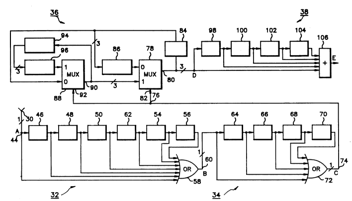
Reference is now made to the circ~lit of Fig. 3 for a description of a
detailed embodiment of the invention shown in the block diagram of Fig.
2except for the temporal spreader 4û which is an optional feature not usually
utilized. The horizontal widener 32 has an input terminal 44 to which a senes ofn c!ock delay elements are connected in series. In this example, six cloclc
delays 46 through 56 are used. The output of an OR gate 58 is connected to an
output terminal 60, and seven inputs of the OR gate 58 are respectively
connected to the input terminal 44 and the ends of the cloc~ delays 46-~6 that
are remote from the input terminal 44. Any control signal having an amplitude
of 1 indicating the presence of a phenomenon such as motion will be repeated
six times at the output terrninal 60.
The vertical widener 34 of Fig.3 is similarly constructed. There are m 1-ff
delays connected in series to an input terminal 62. In this example. there are
four 1-tl delays 64, 66, 68 and 70, so that m=4. The output of an OR gate 72 is
connected to an output terminal 74 and its five inputs are respectively
connec~ed to the input terminal 62 and the ends of the 1-H d~lays 64-70 that areremote from the input terminal 62. Any line of control signals applied to the
input terminal 62 will be r~peated four tlmes at the output terminal 74.
The horizontal widener 32 and the vertical widener 34 are shown as
being connected in series, in the order named, between the input terminal 30
203G175
for the spread~r system and an output terminal 76 for the widener circuits.
HowevQr, as wlll be explained. the ~rder of the horizontal and vertical wid~nerscould be reversed. In ~ither case, control signals having the logic value of 0
pacs through the widener circ~Jits 32 and 34 without any delay and the losic
value of 1, indicating th~ presencs of a phenomenon, is repeated so as to form
a rectansle of logic l's that is n~l clock cyc!es wide and m+1 lines high.
The line signal spreader 36 is coupled to the output terminal 76 and
functions to produce a ramp of increasing signal values along a line that
increases from the value of 0 to a maximum value, such as 7, during the first n
control signal penods referred to. It then holds the maximum value as long as
1's appear at the terminal 76, and when they cease, it produces a ramp of
decreasing signal values along the line over a period of r c!ock cycles. In the
usual case r=n. This is done in the same way along the line whenever the
control signal assumes the logic value of 1, and along the m succe~ding lines
so that there are m+l identical lines.
In the circuit shown in Fig. 3 for performing the line signal spreading
function just described, a MUX 78 has an output 80, an input labelled 0, an
input labelled 1 and a switching control input 82 to which lo~icaJ values of 0 and
1 may be applied. When a logic 0 is applied to the control input 82, the output
80 is connected to the input labelled 0, and when a logic 1 is applied to the
input 82, the output 80 is connected to the input labelled 1. A- one clock delayelement 84 and a generator 86 that performs the function f(x)=x-1 are
connected in series between the output 80 and the input labelled 0. The
generator 86 cannot go below a value of 0. Thus, when no motion is detec~ed
and a logic 0 is at the input terminal 30, logic O's are passed through the
widener circuits 32 and 34 to the terminal 76, and the output 80 of the MUX 78
will be 0. If by some chancs the signal at the output 30 of the MUX 78 should be
20361~ -
other than 0, it will b~ reduced to 0 in at most m cloci~ cyc!es by the operation of
the generator 86. As w~ e seen. the MUX 78 will produca the ramp of
decreaslng values previousiy referred to.
The ramp of inc.e.~sing values, previously referred. to i5 formed by a
MUX 8~. It has an output ~0 that is connected to the input of MUX 78 that is
labelled 1, an input labellea 0. an input labelled 1 and a switcning control input
g2 to which logic values of d or 1 may be applied. As in the MUX 78. a logic 1 at
the control input 92 comlec.s the output 90 to the input labelled 1, and a logic 0
at the control 92 connec~s the output 90 to the input labeiled 0. A one cloc~
delay 94 and a generator g6 that periorms the function f(x)=x+1 are connec~ed
in series between the out,~ut 86 and the input labelled 1. The generator 96
cannot produce a signal value above some seiected maximum, such as 7. The
input of the MUX 88 that is la~elled 0 is coupled to the output 80 of the MUX 78.
The vertical signal soreader 38 that provides the signal values that can
be used by the k-value generator 16 of Fig. 2 to generate the vaiue of k and 1-kfor each pixel location is comprised of means for succassiveiy making available
the signal values for each posltion alons the scan line for which a value of k is
sought and the signal values of positions above them and means for combining
each set of values in ac ordance with a predetermined function.
Ths means for making the signal values for corresponding pixels along
the scan lines available is herein shown as being comprised of m t~H delays.
Delays 98, 100, 102 and 104 are shown so that in this particular ambodiment
m=4.
Whereas the signal values at the output 80 and at the ~nds of the four 1-
H delays 98 through 104 that are remote from the output 80 could be
respectively weighted before they are combined the means for combining them
is an adder 106.
203617~ -
ClR~:l llT ~PF~ATION
The operation of the circuit i ~9. 3 will now be ~xplained by reference to
Figs. 3A through 3E that show signal values that would be present at
correspondingly lettered points in Fig. 3.
For the purpose of this ~xplanation it is a-ssumed that the control signals
applied to the input terrninal 30, which is point A of the control signal spreader,
has only two succ~ssive values of 1 indicating the presence of a given
phenomenon, such as motion, and that all the other positions on the scan line
have the reference value of a logic 0. Such a situation is depicted in Fig. 3A
where these original control signals of 1 that ~ccur along a scan line L1 are
enclosed in a rectangle 108. It is to be understood that line L1 would have
many more signal values than those shown.
Fig. 3B illus~rates the signals appearing at point B which is at the output
terminal 60 of the horizontal spreader 32. This signal includes the onginaJ
control signals that are within the rectangle 108 and n repetitions of the logic 1
of the second control signal vaiue. In this example, it is assumed that n=6 so
that there are eight logic 1's along the scan line L1.
The signals at point 8 are applied to the input t~.",inai 62 of the verticai
widener 34 which repeats the line 1~1 m times. In this example, m=4 so that
logic 1's are prqdvce~ at a point C that are inrlu~ in a rectangle of signal
values having a width equai to the number of contigl~otls control signals plus nrepeated co,,ttul s;gnals and a height of m+1 lines.
If the vertical widener 34 pr~_~ried the holiLGIlt~i widener 32, its output
would be as illusl.~t~J in Fig. 3B', and it is readily a?par~nt that, after these
203617~
signals are applied to the honzontal widener 32, the signals of Fig. 3C will be
produced.
The line signal spreader 36 operates as follows. The control signal
values for all lines including the lines L1 through L5 of hg. 3C are successively
supplied to terminal 76, which, as shown, is connected to the switching control
inputs 82 and 92 of the MUXes 78 and 88. If the output 80 of the MUX 78
should not be 0, the application of a few O's to the terrninal 76 will cause theMUX 78 to count down to 0 and it will appear at the output 80. The output gO of
the MUX 88 will also be 0 because its input labelled 0 is coupled to the output
80 of the MUX 78 as lon~ as its switching inputs 92 receives a logic 0.
As soon as the first logic 1 of the original control signal in the rec~angle
108 reaches the terrninal 76, the outputs 80 and 90 of the MUXes 78 and 88 are
connected to their inputs labelled 1. This means that the output 80 of the MUX
78 is connec~ed to the output 90 of the MUX 88 and that the output 90 of the
MUX 88 is connected to its input labelled 1 so as to receive the incremented
values provided clock by clocl< by the generator 96. After n cloclcs, in this case
6, the signal value is 7, and the generator 96 is such that its maximum output is
7. During the next two logic 1's of the line L1, the maximum value of 7 is
retained. However the next control sisnal value is a losic 0 so that the MUXes
78 and 88 are switched. The output 80 of the MUX 78 is now connected to its
input labelled 0 so that the value at its output 80 is red~ce~t by one at each ciock
count. The generator 86 is such that it cannot go below 0. When another
control signal, which, of course, has a vaiue ot a logic 1, is encountered, the
entire process is rere~te~
Fig. 3D illu~ dtds the output values at the output 80 of the MUX 78 which
is the point D in the circ lit. Each ot the lines is pf~cessect as just desc~ ed so
that they have identical values at c~lldapollJin~ po~itlons.
203617~ -
it should be not~d that the generators 86 and 96 c~uld be programmed
so as to generate ramps that ar~ nonlinear rather than linear as shown, e.g.,
they could be programmed to have different increments or decrem~nts for given
input values.
The operation of the vertical spreader 38 will now be exptained by
reference to hgs. 3D and 3E. As noted above, Fig. 30 represents succsssive
identical lines of values that are presented at the point D which is the input of
the vertical spreader. The output 80 and the 1-H delays 98-104 effectively form
a vertical window such as W1 in Fig. 3D that is one clock cyc~e wide and m~1
lines high. After scanning across the lines, it drops by one scan line and scansacross the next set of lines. In this particular embodiment, the operation of the
1-H, delays 98-104 and the adder 106 will produce a value of 1 when in the
position W1, and this is the value used for the first position shown in Lt. Since
the top four pixels are 0's, the output of the adder 106 will be the same as that in
L1 of Fig. 3D.
On the next scan, the window is lowered one line to a vertical position
indicated by W2 and the output of the adder 106 will be as indicated in L2 of
Fig. 3E. As the window makes su~e~sive scans, the resulting signal values will
be as indicated in Fig. 3E. By way of illustrating, consider what the output of the
adder 106 will be as the window drops vc.~ically one line at a time, beginning at
the position of the rectangle W1. ~he values obtained will be the values of the
first column ~fe~ by the spread~r of this invention. At s~coess,ve vertical
positions the sum of the values within the window will be incremented by 1 untila maximum of ~ is reached. At the next step, the lowest pixel in the vAndow willbe 0 so that a value of 4 will be produced
From the values of the lines in Fig. 30, it is apparent that the sums of the
values within the window will increase a~ shown in fig. 3E as the window
203617S
proceeds from the left to the middle and will decrease as it proceeds farther tothe right. It is also apparent that the sum of the values will increase as the
window drops to the bottom line of Fig. 30 and that it will decreasa as it dropsbelow that point.
The maximum values of 35, emphasized by rectangle 110 in Fig. 3E
indicate the positions of the original control signals in rectangle 108. They
occlJr n clock counts (6 in this axample) plus m lines (4 in this example) laterthan the original control signals. The values of 35 can be made to oca~r at the
same time as the video by inserting the proper matching delays into the video
signal path.
Figs. 4A through 4E illustrate the signal values that wou~d be produc~d
by the control signal sprèader of Fig. 3 in response to a different set of control
signal pulses shown in Fig. 4A. There is this difference, however. hgs. 3A-F
show future samples as moving toward the right and downwards whereas Figs.
4A-E show them travelling to the left and upwards. -Thesa are merely two
different perspectives of the same -si~t~on.
Reference is now made to Fig. 5 illustrating a diff~rent circuit for the line
signal spreader 36. Components and points in the circuit of Fig. 5 that
correspond to Fig. 3 are similarly de~gr,dled. The principle difference are that a
PROM 110 is programmed to perforrn the functions of the generator 86 and the
MUX 78 and PROM 112 is progrd,--,--e~ to pertorm the tunctions of the
generator 96 and the MUX 88. The table ot hg. 5A des~-ibes the ope.ation of
the circuit of hg. 5 in r~sponse to control sisnal values of 0 and 1 that a~pedr at
the terminal 76 of MUX 76 (Fig. 3). Since this circuit s~ a~ the line s;ynals inessentially the same way as the dn:~lit shown in Fig. 3, no further e~ ;tio,l isrequired as will be undo.stood by those ~killed in the art.
- 2036175 --
Although several particular embodiments of the invention have been
described, means other than those shown will be apparent to those skilled in
the art.
16