Note: Descriptions are shown in the official language in which they were submitted.
2~3~2~5
I ~NLN'I`I~ U~'I'IBl.E ~Ol~k'l~ Sll~ JAL l,l~:VEIJ V~L.'I'/~ NI'l!'l'
2 l3~CI\(;I~OUN~ ()l~'`l`lll~' INV~N'I'I~N
3 'I`he pre~.ent invention l~elates to a stnnd~ .c. I~o~er
~ supply havin~ ~n inverl,e~r that, l~ill operute l'rolll eilhen ,.r
~,wo levels of d.o. ~olt.a~e.
Unintel~ruptible power systems, Ol~ UPS, are a~ai l.al. l.e
hich are based on se~eral different topolo~ies.
8 For the most senslt:ive loads, the full tinle in~erl nl`
9 or "true UPS" approach is best. ln this topolo~y, an
inverter supp]les a.c. to the load Otl a continuous bLlsis .
Il When the a.c. power line is available, the d.c. po~er
12 required by the inverter is supplied from the a.e. Iin~
13 (via rect:ifier/battery chnr~er). l~ilen t;he a.c. Iine is not.
l~l available, the d.c. po~er requiled by ~,he inverter is
supplied by batteries. 'rhese ba~teries are rech~r~et~
lG the re~tifier/char~er ~hcell tl)e ~.c. line is again
17 available. Since ~,he in~ert.er always supplies pol~er to 1 he
~8 loull, I;here is a~sol~ll,ely no inl:e~ upl;ion or dist~ nllee c-l`
19 the a.c. output when t;he ~ol~er line Fails or l~et~lrns.
'I'he disadvanl,a~ s to 1,hi9 al~pl`OaCh al'('` cosl, rln~
21 efficiency. Normally, all c~c`-the po~er re~luire~l b~ ~he
2~ loacl,~oes l,hrough two po~er eonversions: from a.c. to d.c.
23 (via rectifier/cl1arger) and then from d.c. baclc to a,c.
21 ~via the in~ert,er). The ad~antage is that there i~
absolutely no disturbance in -the output, ancl the output
`2~ Frequency is indepen~ent of the input. This is a
'27 l~articular advnn~a~,e ~here the loa~1 is freq~lenc~ senxi1i ~'f:'
28 and the input powel is unstable ~as in some thir~
29 countries or when operating off of` an emer~ency ~enerato~
or ol,ller such soutce). Th;s also allo~s tlle llP,~ lo ~e use~
31 as a frequency converter, such ns l~hen a 60 Hz load i5 -to
32 be operate~ on a 50 ll~, power system. ~lso, no swil.-:hin~ is
33 required to ~isconnect t;he input to the UPS from the fai le~
2~3~?,~
I i l~ e i x ~ 1' I,I)e i r~ r f.e ~ l'f~-~(l i ng
2 l~ot~er back t.o the inpllt..
') t)ne nf Ihe reasons for poor effic~ieney ;n the l:rue UPS
1 irl smnller s.i7.es iS t.hf.? u~e c f lo~ VC)It.Agf? ~nt.teries. ln a
.-~ sl~ y.~ ttl?r~r vol~.r~f? l~il.]. f~ellera~ y ~e in tl~f.?
Il 12 I.O 3~ volt r~n~f~?~ Th:i~ .iS trUe for pr.imarily eeonomif~
~ l-e7.~solls. E3~.~tl;eries are mncle Up of ind.ividual cells~
~t e~~)nl~fe~f3d il~ Sf~ries. A t.yl~;enl .leAd ~c~.id battery ~e]..l has
r~ n~mi.na.l. vol.ta~f ot` 2 vol.ts, thus a 12 volt bal;tery has
It) xi~ cel.ls, n 2~1 vo.lt hal.tery hns 12 cells~ nnd ~o on. For
~ ,r~ Ar~ ~llll->llr)~ r f~rlf~rgy sfi~nr~n~r~f?l r~e f~ln IIX-~ r~f?lflf..i~ r
I ~ re,~ l~r~e c~el].s (IOW volt.a~e, hi~fth current), or R ~r~re?nter
~ llnrll il.y Or SlllSlllf?r cel.l.s ~hi,r~ther vol.l;a~e, lo~er cllrrent).
.\1 Ih~-~ rel~t.lvfly J.ol~ inower levf-ls of :int.erest here, t.he
I.l.se ol` rf.~lnli.vely fewer, lar~er cel.].s is m~lch less
e~ensi.ve thnn .17~r~e number of sma.ller cells-
r)rfrl;lln:ll;el.y, l~ower cnn~er~.i.on at. ]oi~ voltage and hi.rath1~ elll~l~f.lll i.x m~loll less ef`f3.ci.ent; t.llan pol~er C~onversion nt
l~;J ili,f~lll?r` voltage lln-l IOI~er cllrrent. ~em.i~onductor con-.l~ftion
~0 IC-XSf?S of ~ .O volt, for e~nmp.le, are very si~n:if.ic7.1nt on n
21 12 vnlt system~ bl.lt mlJoh lf.?SS so on a 2fiO volt system.
c)m t:hf* Ul~ r~es~tner~s viewl~oint, it iS des.ire~ble tc-
'2:3 use n d.l~. vol t~e i n ~hf.? 100 200 volt ran~e. From a cost
2-1 v.i~wl-oin1:~ thix is not prnct:ical in small syste1ns bf~?cause
~,F~ ~r t.hf? cost. o~ thf? hatteri.es.
~ If~lf~ .Y _ r ~ l N~IFNll'T~N ~i
27 'I'l~f? ~ f tll-~ ?xf-~nf~ in~ rl~if~n i.~ t.~
'~ IllI?nllS for a UP~ to operate at a high d.G. vol tarate, ~hile
29 llsing lo~ vol ~,a~e bat.ter;.es. ~y way of explanation~ it
:~0 sl~olll.ll be not.e~l l;llAt 1 he IIPS .is operated from t.hf? a.c. line
3lal almost nll times. I:lal,tely l~ower is used only l~hen the :~
n . e . 1 i ne i s unavai lahl e, an(l even in areas hThere power
3:3 r el iabi l i.t.y ;s very l~c,ol, the line .is availabl.e at least
3~% of t.he time (~ full hollr of ~-ower fa.ilures each ~~ef*k
-3- ~ ~ 3 ~
~ e ~.1% av;~ ;ty). lt. is, therefore, t.he
2 et`fi(.~i.f?ncy of the system i.n ]ine mode which is of concern;
el`l' i (` i ellCy i n i ~IVerl.el' mocie .i X Or I it,t;.l.e .importance.
I 'I'he UP~ topolosy d;sclosed here.in has an inverter
~) Wll i ~l~ O] t~l.`A t,(~s A t t,l~n difrf?r~?n1; ~l.c. voltn~es: A hi~h
~; vol.I:a~e i.n .I.i,ne m-)-l.e, und a .l.oI~ volta~e in haI;ter~y mode.
7 ~ ? i ll \~ '.e r :i. n c~ ld e ~; ~1 t rfl n g Fo rme r ~ v .i r)l~ Fl rlr i mn r,Y
~inclin,L~ aIld rl st.?corl~Mry willdi.Il~ the pri.mAry winclLnst bein~
~I divi-1~!~1 int.o nt :Ienst. three portions.
Il) It, nlso ino1n.l-les a first d.c. source applied
II nIt-?l~na~.el~ ncr~ss a fi.rst .less t.han a~.l porti.on~s of the
12 I-r;lllarY l~;nr~ An(3 I,l1en aCrOS~ n seconcl l.ess than ~1.1.
:l porî ions Or the primary I~i.n~lin~, t.he first an~ ~second .1ess
I;l IhAn nlI. por~,i.c-n.s havirl~t n common port.ion.
1~ :In n-3dit.ion, it. ;nclu~es a second d.c. solIrce apll:ied
II. n1tel~n~tin,¢.1.y across at least a port.i.on of the c.?ommon
17 por~.ion when the first d.c. source is less than a
Ih l~r~ 1ernl;ned VQ1I:a~Lre~ ~S a res~ ,, thf~? secondary ~indir
I~ ;x m~lintnined at. a rf;?lnt.:ivf?J.y constant a.c. volt.a~te.
~ ! X~?~Orl-.l cl . ~` . X-)ll l`C~? Ill:,ly 1~ . i f?~3 Fl 1teT~n~lt.ill.~tl~
'>1 acrnss the at..1.east. a portion of the common port.ion .in a
'~2 o-anl:.er-tal)ped .invf?rter conf`i~gurati.oIl~ the at least A
2~ poI~l.iorl of t.he common portion havins~ a center tap.
2I 1`he predetermined volta~e i.s determ;ned ~S~ when a
2:~ vt.)1ta,Lt,e at: I.he center-tnp drops below that. of the xecon(1
21~ d.c. source.
27 Alt.ernat.ive1.y~ the second d.c. ~ource may be app1.ied
2~ ~.1t.ernat.in~tl~ across t,he ~t least a port;on of the common ~.
`2!~ porl:i~,n in an ll-hri-l.Ltt~ inver ~,er confi~l~ra~,ion, t.he at. Ieast.
:3f1 n l--rI:it)n )f t;he common portion havin~ a voltase at each
:31 end ~.he~reof.
~2 rn this case, the pre-leterminell volta~e is determi.ne~
y ~h~?n hot.h en~ volta~es ~rop belol~ that of the second
3-I d.c. source.
`,
~3~
l.~R:IEI~ XCI~.II''I`:t~)N 01` 'I`Hh DRAWlNG~
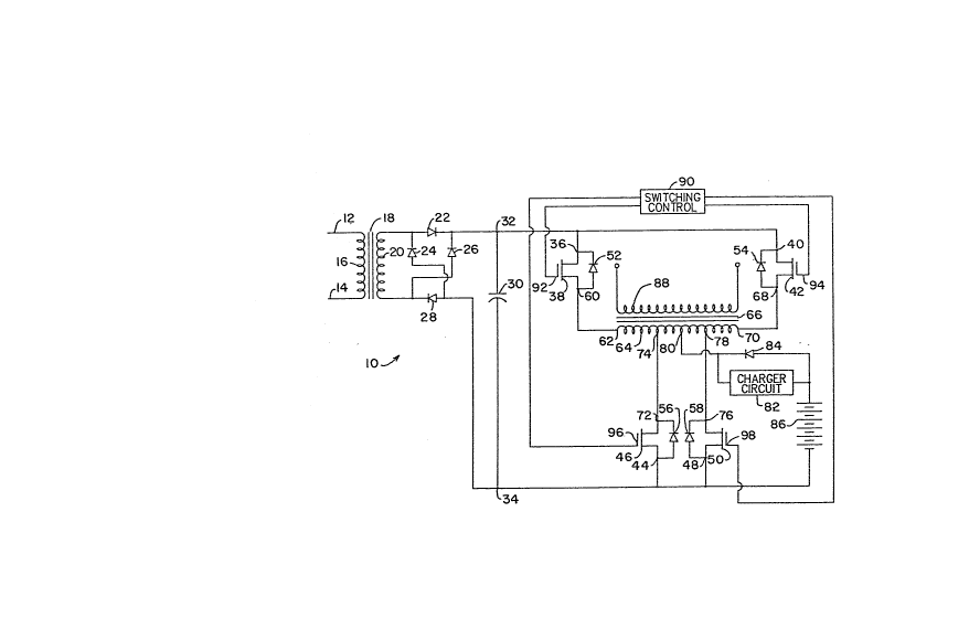
5~ G. 1 ;.s a schematic dia~ram o~ an uninterruptihle
ow(?r s~ p~ aoeorcling to the ln~ention.
~ '1(3. '~ i.x a sc~51emntic dia~l~an1 of.' anot5~er embodimen1; o1`
fi nn ~1nin1:err~ le l~ower ~ ply a~cor~lin~ to tlle invent;on.
~; 1)f~ ,lP'1'10N Oi~ l'HE ~RE~h' Rk'1) 1~:~15~0Dr~1fi'N'1'S
7 1~eferr;n~ to 1~.[a. l, an uni.nterrupt.ible pc~er s-1pply
R noeorc1ing to the invention is generally indicated by the
~ n11mern.1 10.
111 .~n n.~. 1ine t2, 1~1 is norma1..1.y connected to the
11 ,1>~im~r~ in(ling 16 of ~ l:rnnsformer 18. 'I`he seoondAry
~ inrlin~ 20 is connectetl to the hri~e dio~es 22, 2~, 2fi, 2~ ~ ,
13 t~hich are connected .i.n a f'ull-wave bridge rectifier
1~1 eonrig~1rat.io1~ '1'he onl)aci.1:or 30 i~ connected across the
lF d.c. OUtp~1t t,erm.inals 32, 3(5 of the bridge diodes 22, 29,
1~; 21;, 28.
17 ln operat.ion, a cl.c. volta~e ap~ears at the termina1.s
1~ ~2, '~ hen the a.c. line 12, l~ .is energ.ized. It, is of
1t~ e-1lrse ~ossible t,o substit,ute other d.o. sources at the
t.e~nminnl.s 32, 3~. lt. shol1ld be notecl that t,he ~alue of
~1 ~.his -1.c. volt,~e c:~n be mnde as hi~11 as des.ired for
22 effic.;ent inverter operation. For e.~rample, a vo].ta~e
2:~ within the range of lOO-200 volts has been found to offer
2:1 si.~ni.fi.cant efficienoy advantages. :
2~ The termina]. 3? is connected to the terminal 3~ of t.he
2~ it.chin~ element ~8 and to the terminal ~0 of the
~7 s~it.ohi.n~ el.ement ~12. 1'he termina]. 3~ i3 connected to the
.e~1ir~ 1 c-f the s~.it.ohin,~ element 46 ancl t:o the termir1al
~ 3 ~ in,~ ?lll-?ll 1: ~ n .
:10 '1'hl~ s~il.e11i11,~ elen1ent,s 3~ , 5n may be, fo
3I '`.;~1111~)1~, 1`ie~ -(?I`r-?-`t. tr-lnsistors as s5~o1~n, or hi~1.a
3" t.r~nsixt.ors, or ~C`~s. '1'he diodes 52, 5;1, 56, ~8 are
:
-5- ~3~
2 ;38, 12, 1~, ~0, respectively. In the cnse of field-ef~`ec1;
3 tr~nsistors the diode is .integral 1~it1- the transistor. If
~l oll)er tyles of s~;.t:chin~ e.lements are used, a se~arate
5 ~liode is ~1setl.
I; 1`ll(? I f?l`llli.ll~ 0 of l:l1t-~ sl~itch;~ e.1.e~ nt 3~ is
7 ool~nectl-cl t.o th~-! e1l~i t~1- fi2 oF the primar~ wind.in~ 6l1 of a
8 tll.1rlsrorrner 6fi. Ihe terl11.ina.1 ~ of` tlle s1~itchin~ element
tl 12 is t.~onnecte(1 I.o the ~n-.1 t;np 70 of the primary w.indir
1 () 1; ~1 .
11 I`he l:erminul 72 o~ the sl~itchin~ elennent i16 is
~2 connec-t.ed to 1:he in~ermediate tap 7-1 of the primary winding
13 fi~l. l`he terminn1. 7fi of the s1~.itchi.ng element 5() is
1~ fil.
Ifi The center tap 80 of the primary winding 61 i~
17 connec1ed to the inl1lt of a charger circui-t 82 and to the
18 cal;hode of a di~nle 81. The output of the charger circuit
19 ~2 ancl the anode of the diode 8~ are connected to the anode
of n battery 8~. rhe cathode of the battery 86 is
21 oonnected to the d.c. output terminal 3~. The battery 86
22 mn~ be, for example, a 12-volt rechar~eable battery.
2~ The transformer ~6 is provided with a secondar~
21 ~.inding 88. Where good regulation and sinusoidal output is
2~-. iml-c-rt.ant., the t.ransformer 66 would be a ferroresonant.
2l; I:rans~ormer, otherw;.se a cnventional. iso].uti.on transformer
27 is n~1e(~ te.
2X ,\ s~ chin~ conl:ro1. 90 ~rovides sw;tching contro~. :
2~ si~rll1ls ~.-) Ihe conl.l~o1 in~ l.s ~2, 9~1, 9fi, 9~ of ~w.i.tcl1in~
3() e1ements 38, ~2, lfi, .60, res~ectively.
:;1 N-~rmn1ly Ihe l~ower ~su~ y 10 ol~ernte.s ns n sl;ra.i~11t.
32 f--:wnrd H-hrid~e inverter. When ti1e u.c. line 12, ~.;1 is
33 ener~ized, ~ d.c. ~o~ta~e appears at the d.c. output
3~1 termi.nals 32, 31. The Sl~i tching control 90 provides
~5 cont:ro.1 signals to the ~sT~itchin~ elements 38, ~12, ~16, 50
3f; sl.lch that, alternal:ely the s~itchin~ e].ements 38, 50 conduct
. ~ . ~;, . .'
: :,: - ~ .
'-6- ~3~
\~ ile 1.1~1~ s~ in~ e.l.~ nl.s 1~ 11; ul~e rlonc~ ll.lel~in~ Ullll '
2 then the s~itchin~ elements ~2, :16 conduct and the
3 switchin,¢ elemenl;s 88, :, n are nonconductin~. 'I'his rel>eats
e rlesil(!~ fl~etluenc~. 'I`hlls, tl-e ~.c. volta~e nt the
fi ~I.c. olllpul: I;el~mirlllls .~2, ~1 i.s apl)lie-l all:ernatel~ acl~osq
l,~lr~ r~l~illll~r~ illtli~ et,l~ell 111~ cllcl tr~
7 62 ~nrl tl~e in~,e~mediul:e tnp 78 and the ~ortion betl~een t.he
8 end tap 70 alld t,he int,ermediate tap 7~. 'rhis results in
9 the desired a.c. voltage at the seo~ndary ~indin~ 88 bein~
~ ro~
I1 'I'he position of the intermediate taps 7~, 78
12 det.ermines the volta~e at the center tap 80. 'I`he
18 intermediate taps 7~1, 78 are positioned ~o that the vo]t.a~e
11 pro~u~ed at the oenter tnp 80 is, under normnl a.c. line
IS volta,¢e con~ition~ on tl~e a.o. line 12, 1~, a d.c. vo]ta~e
16 somel~hat hi~her than t.l-e voltage of the battery 86, for
17 e~mple, lO percent ~renter.
~ s l-nl~ ns l:he volt.a~e at. lhe cent,or tap ~0 i9 hi~he
l9 than the volta~e of the battery 86, the diode 8~1 bloclcs
2() current flo~ from t,he center tap 80 to the batter~ 86. 'I'hc
21 chnr,~er Ci.l`Cll.it 82 allo-~s a portion of the current from the
22 center tap ~0 to mair,tain the battery 86 in a charged
2~ st.~t~.
21 Tf t.he volta~e on the a.c. line 12, 11 drops too far
2& lor fails compl~tely), the d.c. voltage at the d.c. Olltp-lt
21; ~2, :l~l he~ins to drop~ As this ~olta~e drops, the ~olta,~e
27 at ~l~e center tap R0 a~x~ drops. At some point, t.he center
,np ~o]ta,~e drops beJow the volta~e of the battery 8~, and
elllrent is nble t.o flo~ hro~ h the diode 8~.
3~ Tn this s1:ate, the s~itchin~ elements ~6, fiO are
31 f`llnctionin~ as part of a center-tapped inverter circuit
32 ~also kno~n as a parallel in~erter). The volta~e of the
33 I-~tt.ery 86 is applied a]ternately across first the portion
3I r~l Ihe primary win~iin,~ ~l be1,~een the center tap 80 and the
interme(l;nl,e t~p 7~1 and t,hen bet-~een the center tap R0 and
3fi t,he intermed;ate t,ap 78. This repeats at the desired
, .
'
_7_ 2~
I I r~ ql~eno~ . 'I'lli.s resul l:s irl l;he ~esired a.c. volta~e al; the
2 s(?~onda~ w:indin~ ~38.
3 'I'his can perhaps best be visualized by ima~r~inin,,~ that
1 ~.he swit,chin~ element.s 38, ~2 and the portions of the
6 .~re no loll~er ~resent.. 'rhe com~onents are of co~1rse still
7 ~1~esenl;, hut l;he;.r onl,Y effeot in l:.his mode of op~ration i.s
Ite~p t.h~ ~a~ci.t.or ~'~0 ch~lr~ted.
g 'I'he re~.1Jrn of suf~i.ci.ent a.c. line volta~te ~ill boost
~ I . C . V t - 1. 1. ~l ~ ~` I I I . I . I I ~! l. ~! l` lll .i I I 1~ 1 S ~1 2, 39; ~ o.1~ e ol
11 t11e center ta~ 80 ~ ..1. .i.ncrease to re~erse b.ias the diode
12 89; the ~ower SIJpp~ 0 ~ill resume functionin~t as an H-
1:3 hri~e i.n~erter an~ the char~~er circuit 82 will rechar~e
1.'~ It shoul.d be note~ that the chan~eover from A hi~h
lfi ~o.ltage H-brid~e to n center-tapped inverter operatin~ from
17 a lo~ o.l-ta.te battery takes place qu.ite naturally and
~ 1ltolllr~t.ic~ ly, wiL11 no Chall~'f' in l.hC` eonLrc)l s.i~nals from
19 I:he switc11i.n~ contro1. 90 req~1ired. No ~olta~e sensin,g or
'?() SW:i t cll~in~t of an~ 1tir1d is re~uired.
21 Referrin~ to FIC. 21 another embodîment of an
22 ~Inillt.errl11:)t;hl~ lower s~ ply accordin~t to the ;nvention .is
2:~ ,~enern.1.1.y indicate~ by the n-lmeral lO'.
2~1 rnsteacl of t.he cat11ode of the ~iode 8~ and t.he inp~lt
of the char~er circuit 82 hein~ cor,nected to a center tap
2fi of the ~r.imar~ windin~~ G~l as shown in FIG. l, the~r are
27 connected to the terminal lO0 of a swit~hin~ element 102
28 an~l to the termina]. 109 of a switching element 106. ,~s
29 IJith t.he switc11ing elements 38, 921 9~, 50, the switchi.n&~
~h ~1emen1.s 1n2, 1n~ mn~ he, for e~am1-1e, fie.1d-eff-ect
:11 ll~n.si~tor. as s.llown, or bipo].ar transistors1 or SCRs. Tlle
32 (1iol1es 108, 1:10 .nre oonneo1;e~ :in in~,rerse ptlrallel wi1:h the
l ~ swi I,clli nLr~ element.s 102, ln~ res1~e-:ti~e1~. Thl? termi.na1. 109
'~1 Or the xwi l.chin~ e.1eme11t 102 ;s connected to the
~ in~ermerli.ate t.ap 7:1 an(:l the t,erminal 11l of the switch.in~
:~.fi e] ement 101~ is connectet3 to t.he ;.nt.ermed.iate tap 78. In
- -8- 2~2~ -
~ .. r r ~ .. f ~ r~ t.~rnl
~ wilh thc i;rnnsi~sl.or. ll` olller types of s~itchi.n~ e.lemen~s
3 ~re ~.~se~, a separate diode i~ ~sed.
s~itchin~ contro.L 90' provides switching control
~:ign11.s to the oontro.l. inputs 92, 9~, 96, 98, 112, ll-l of
6 s~i.tching e].emQnts 38, 12, ~), 50, 102, tO6, respective1y
7 No~mall.~, tll~ po~er xllpp.:l.y tO' operates a.s nn ll-brid~e
~1 inverter. When t;he a.o. li.ne 12, 1~ is ener¢.ized, a d.c.
9 voltage appears at the d.c. output terminals 32, 3~. lhe
In .s~itchi.n~ contro]. 90' provides control si~nals to the
1l s~itchin~ elements ~8, 12, ~6, 60, 102, 106 su~h thnt
12 al.ternate].y the switchin~ elements 38, 50, 102 conduet
13 ~hi.l.e the s-~itchi.n~ elements 92, ~6, 106 are nonconductin~
11 nnd then the switchin~ elements 12, ~6, lOG conduc1; and the
l~ s~itching elements 38, 50, 102 are nonconductin~. This
1l, repeals at t:he desired fre~ enoy.
17 As a resu.lt, the d.c. voltage nt the d.c. output
l~ lerminals 3~ nppl.ied a1ternn1;ely across the port;on :
l4 ol` ~ e primary l~;n(l;n ~1 1etween the end tap 62 r~nd the
21) in~.errni?dial:e tap 78 and the portion betl~een the end tap 70
2l ~nd the intermediate tap 7~1. I`hi.s reslllts in the desired
2' n.c. vo].tn~e at the secondary wind;n~ 88 bein~ produced.
2~ ~t the same t:ime, the s-~itchin~ of the ~witohing
21 element.~ 102, 10~ provides a portion of these vo.l.1:a~e~ to
2~5 t:he d.iode 8~1 and the char.~er circuit 82. In pnrticular,
2li ~hl~n Ihl ~l.l.n~e fr~m t.he terminals ~2, :~1 ;.s nppl.ie~
, ncros~ the portion of the primary w.indin~ 6~ between the
>R en~ p 62 and the intermediate tap 7~, the intermediate
29 t:np 7-l is c~nn~cted 1;o the diode 8~ and the charger circuit
:3l1 ~2. Similar].y, when the vo].tage from the terminals 32, 3;1
31 is app1ied across the portion of the pri.mary winding 6
.3 ~ hl?l l~een t.he enrl tap 70 an-l ~he intermediate tap 7-1, t.he
~:~ i.nt.ermedi.~te t.~p 78 ;s connected t,o the diode ~ and the
3 1 cl)ar~er ci rcui t 82 .
3~ The po~sition of -the intermediate taps 7-l, 78
let.erm;llcs i:he ~o1t.n~e l;hnt the sl~it.chin~ elements lO2 IOfi
~e3~2~
g
2 in1:ermedinte taps 7~, 18 are posit;ioned so that the ~olta~e
3 1~ro-1uce~ at. the dio~e 8~ is, 1n~er normal a.c. line volta¢e
1 con~1i1;.ions on 1;he a.o. 1.ine 1~ 1, a 1.c. vol ta~e somewl~a t
i,~hC?l` than 1.he vo]ta~¢e of the In1:tery F36, for e~ample, tO
7 .~s lon~ as tllf` ~olta~e Ut 1he cathode~ ot` the cliocle 8;1
R i.s hi~11er thnn t;he volta~e of the battery 86, the ~iode 8~1
~ b1Ooks current f:1.o~ fron1 1;he intermediate tnp-q 7'1, 7~ to
t.he 1~attery Mfi. l'he char~er circlli.t 82 allows a portion of
11 11le ~urren1. from the i.nter1nediate taps 7~, 78 to maintain
12 t.1)e hattery ~ in n charged state.
13 Tf t.h~ vo1~.a~ on th~ a.c. 1.in~ 12, 11 drop~ too fa
1~ :3., 3~1 he~ins to ~Irop. As th.is volta~e drops, the volta~e
11i a~ the cat1-ode of the .liode 8~1 also drops. At some po.int,
17 this vo.lta~e clrops belo~ the volta~e of the bat-tery 8fi, and
18 e~1rre11t. i~ nh.le t.o flo~ t.hrou~h the diode ~.
I') rn this state, 1;he s~itohin~ elements ~fi, 60, 102, IOfi
are functionin~ as part. of` an H-bridge inverter c.iro~1.it
2I pca~ered by 1.he ba1;1:ery 8~. 'I'he volta~e o~ the battery 8fi
22 i.s alplie~l ~lternatin~ly across the port.ion of the primary
23 1~indi.ng fi-1 ~et~een the intermediat.e tap '1-1 and the
'>1 ir11:1?rmedirlte tnp 78. '1`his repeats at the ~esired
2~-, rreq1.~er1cy~ This results in the desired a.o. volta~r? at t.he
2(. seel~n(1nr~ ;ndin.~ 88.
27 'I`l1e return of sufricient a.c. line volta~e wi.1.1 boost
28 the d.c. volta~e at the terminals 32, 34; the volta~e of
29 ~ e cathodf? of the diode 8-1 will increase to re~erse bias
3~) t.hf' diO~f~? 8~; the power 511pp~ 0 will resume functioni.n~
'31 ~ith power from the d.c. output terminalq 32, 3-1 and the
.'>2 ell')r~er Cil'Cllit. 82 ~ill rechar~e the battery 86.
:1:1 The en-l:)odiment of ~IC. 2 i.s useful 1~here more
31 i111.ern~e~1if11e hat.tery ~oIt.a~es are 11~ed (e.g. 36--~8 ~o]t.s)
3~- ~eca11~e the ~->l1;age dolJb].ing effect of a center-tapped
.:. , .. ~
. ~ :, ~. :, .... .
-lo- 2~6~
I It. should ~e evi.(lenl: ~hRt this ~isel~sllre is by way of
2 e~ample and that var.ious chan~es may be made by add;n~,
3 modifyin~ or eliminat.ing de-tails wi.thout departin~ from the
~I fair scope of the tenchin~ oontained in this disclosure.
r) ~l~he invent.ion i.s t:herefore not, limi.ted to pnrticular
1> details of l;h.is di.scl.osure e~cept to the e~tent that the
7 I`ol lowin~¢ Cltlims al~e necessarilv so l.imitecl.
.,
' . , ' ' .: ~
:: :. . . .
.: