Note: Descriptions are shown in the official language in which they were submitted.
~ I - 20~-~342
PROCESS AND APPARATUS ALLOWING THE REA~-TIME DISTRIBUTION
OF DATA FOR CONTROL OF A PA~ K~l~G PROCESS
Field Of The Invention
This invention relates to an electronic data loading and
distribution system and, more particularly, to a system
using a programmable direct memory access controller for
the real-time selection of destinations for digitally
encoded data.
The system may be used to control the selective
application of dyes or other marking materials to a
moving substrate in accordance with digitally encoded
pattern data. The programmable direct memory access
cu,.~oller allows multiple patterns or repetitions of the
same pattern to be generated by a pattern control system
across the width of the substrate in real-time as opposed
to being generated off-line and ahead of time.
Background Of The Invention
This invention, in particular, finds application in the
field of textile dyeing. A known modern textile dyeing
apparatus includes multiple arrays, each comprising a
plurality of individual, electronically addressable dye
jets. Each of the dye jets in a single array outputs the
same color of dye. The arrays are positioned in spaced
relation across the path of a moving substrate.
Using such apparatus, the pattern-wise application of dye
to the textile materials or substrates requires a large
- quantity of digitally encoded pattern data which must be
sorted and routed to each of the individual dye jets
comprising each of the arrays. Each of the arrays of dye
jets extends across the width of the substrate path~as
the substrate moves under the arrays. It has been found
advantageous to coll~rol individually the time period
during which the dye streams produced by the individual
dye jets in a given array are allowed to strike the
- , . . ........................................ . . . . . .. . ~ .
- ,, ; ~ ~
2036342
substrate. This allows for shade variations to b~
produced from side-to-sidQ (and end-to-end) on the
substrate by varying the quantity of dye applied to the
substrate along the length of a given array.
One such cG,ILlol system capable of providing this
capability is described in co-pen~ing U.S. Serial Number
327,843, entitled "DATA LOADING AND DISTRl~ull~G PROCESS
AND APPARATUS FOR CONTROL OF A PAil~h~l~G PROCESS", filed
on March 23, 1989, the specification of which is hereby
incorporated by reference. This system, which is
applicable to a variety of marking or patterning systems
wherein large quantities of pattern data must be
allocated and delivered to a large number of individually
co~ ollable imaging locations, pro~esces pattern data
received from a real-time ~G~e~Qr through the use of
specific electronic circuitry which accepts the pattern
data in the form of a series of 8-bit units. Each of the
8-bit units uniguely identifies, for each pattern element
or pixel, a pattern design element to be associated with
that pattern element or pixel.
The term "pattern element~ as used herein is intended to
be analogous to the term "pixel~ as that term is used in
the field of electronic imaging. The number of different
pattern design elements i8 equal to the number of
district areas of the pattern which may be assigned a
separate color.
The term "pattern line~ as used herein is intended to
describe a continuous line of single pattern elements
ext~nA~ng across the substrate, parallel to the
patterning arrays. Such pattern lines have a thickness,
measured in the direction of substrate travel, equal to
the maximum permitted amount of substrate travel under
the patterning arrays between array pattern data updates.
, . . . . . ............... _ .. . . . . ~ , . . . . _ , .
., : . - . ; . - ,
20~312
In this system, the pattern element data must first be
converted to "on/off" firing instructions, (referring to
the actuation or deactuation, respectively, of the
individual dye streams produced by the dye jets). This
is performed by electronically associating the ~raw"
pattern data with pre-generated firing instruction data
from a computer generated look-up table. The raw
patterning data is in the form of a sequence of pixel
codes. The pixel codes merely define those distinct
areas of the pattern which may be assigned a
distinguishing color. Each code specifies, for each
pattern line, the dye jet response for a given dye jet
position on each and every array. In this system the
number of arrays equals eight; therefore, each pixel code
lS controls the response of eight separate dye jets (one per
array) with respect to a single pattern line.
The raw pattern data for a given array is preferably
arranged in sequence, with data for dye jets l-N for the
first pattern line being first in the series, followed by
data for dye jets 1-N for the second pattern line, etc.
The complete serial stream of such pixel codes is sent to
a firing time converter and memory associated with each
respective array for conversion of the pixel codes into
the respective firing times.
Each firing time converter includes a look-up table
having a sufficient number of addresses so that each
possible address code forming the serial stream of
pattern data may be assigned a unique address in the
look-up table. At each address within the look-up table
is a byte representing a relative firing time or dye
contact time, which, assuming an 8-bit value at the
address code of interest, can be zero or one of 255
different discreet time values corresponding to th~
relative amount of time the dye jet in question is to
remain "on". Therefore, each specific dye jet location
2036342
on each and every array can be assigned one of 256
different firing times.
The firing time data from the look-up table for each
array is then further proreCce~ to account for the
"stagger", e.g., the physical spacing between arrays, and
the allocation of the individual firing instructions for
each jet in the array. Finally, the individual firing
instructions for each ~et in the array are sent in
parallel to the jet dyeing apparatus for actuation of the
individual jets in each array.
These systems require a full line of pattern data to be
stored in the real-time pro~ec~Qr memory for output to
the pattern control system. When it is desired to
generate different patterns or repetitions of the same
patterns across the width of the substrate, each pattern
to be generated must first be converted into a "full
~ machine width" pattern line. For example, the individual
corresponding pattern lines of each of three separate
patterns must be combined into a single set of composite
pattern lines which individually extend across the entire
substrate. Because this combining of pattern data into
full width pattern lines i8 a computationally intensive
process, it must be done "off-line" from the operation of
the dyeing apparatus. Further, the entire pattern must
then be written into memory which requires an extremely
large memory.
One alternative to formatting the patterns off-line and
producing the patterns in an "across the width" format
would be to eliminate the "full machine width" conversion
process and simply produce each individual pattern, in
real-time, down the substrate rather than across.
However, it is readily apparent that a tremendous amount
of the substrate would then be wasted. For example, a
twelve foot wide substrate used to produce a pattern only
- 2U363~2
three feet wide, such as would be suitable for a hall or
"runner" carpet, for instance, would waste the remaining
nine feet across the substrate width.
There is therefore a need for a process and apparatus
which produces multiple patterns or repetitions of the
same pattern across the substrate in real-time. Further,
the process and apparatus should be capable of producing
the pattern beginning at any point along the width of the
substrate or be capable of starting the given pattern at
any point in the pattern for proper centering of the
pattern across the substrate and thus not delivering dye
to the edges of the substrate.
Summar~ Of The Invention
The present invention overcomes these problems with the
use of a programmable direct memory access ("DMA")
controller to assist in the real-time selection and
production of multiple patterns or repetitions of the
same pattern to be generated across the substrate. The
individual pattern data may be stored in separate memory
locations which are then accessed in any desired sequence
upon demand by the DMA controller. As ~i~cllcre~ above,
the control system is believed to be applicable to a
variety of marking or patterning systems wherein large
quantities of different pattern data must be allocated
and delivered to a large number of individually
controllable imaging locations, and is not limited to use
in connection with the patterning devices disclosed
herein.
In a preferred emho~iment using the present invention,
the programmable DMA controller, without intervention by
the real-time processor, retrieves the same pattern data
from memory a desired number of times to repeat the
pattern across the width of the substrate. The DMA
- 5 -
2036~2
controller operates in real-time to combine the patterns
into a full machine width pattern line for output to the
pattern control system. Thus, unlike systems of the
prior art, only a single copy of the pattern data need be
stored in the memory to produce a repetitive number of
the patterns. This results in a dramatic reduction in
the size of the memory associated with the real-time
processor used to store the pattern data.
The control system of the instant invention uses the
channel select lines provided by the DNA controller to
selectively enable in real-time one of a number of
different destinations for the data output from the
real-time processor. Because of this capability, an
alternate embodiment of the present invention provides
for the DMA channel select lines to select one of a
plurality of look-up tables associated with each array in
conjunction with the retrieval of different patterns from
~ the real-time processor memory. Thus, each pattern that
is combined into the full machine width pattern lines
will have its respective coY~e~ look-up table of firing
times available when the pattern data is procecee~ by the
pattern control system. This allows multiple different
patterns, or portions of a larg~, overall pattern (which,
by dividing the pattern into areas which individually
require no more than 2S6 pattern elements, will allow use
of more than 256 pattern elements in the overall pattern)
to be produced across the width of the substrate in
real-time.
These and other advantages are provided by proper
~LG~ amming of the direct memory access controller. It
is thus possible to change the pattern sequences
"on-line" which results in a savings in time, substrate
material, and memory.
- 6 -
203634~
Details of the present invention herein, as well as
additional advantages and distinguishing features, will
be better understood with reference to the following
figures.
s
Brief Description Of The Drawings
Figure 1 is a block diagram illustrating one pattern
control system environment in which the present invention
may operate;
Figure 2 is a schematic block diagram illustrating in
greater detail the real-time computer and pattern control
system of Figure 1 and, more specifically, illustrating
the programmable DMA controller's interface with the
pattern control system of Figure 1.
Figure 3 illustrates an example of two patterns and their
~ associated look-up tables stored in the real-time
computer memory.
Figures 4 and 4A illustrate portions of a substrate
patterned in accordance with the examples of Figure 3.
~etailed Description
For purposes of this discussion, the programmable DMA
controller and control system of the present invention
will be described in conjunction with the jet patterning
apparatus discussed above and to which this invention is
particularly well suited. It should be understood,
however, that the operation of the programmable DMA
controller and control system of the instant invention
may be used, perhaps with obvious modifications, in other
devices where similar quantities of digitized patt~rn
data must be distributed in real-time to different
destinations.
2036'~
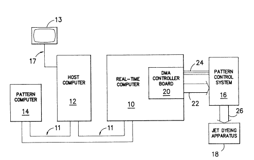
Referring to Figure 1, a multipror~c~?r patterning system
5 is shown having a host computer 12 coupled via a bus 11
to a real-time computer 10. Optional pattern computer 14
is further coupled to the host computer 12 and real-time
computer 10 by the bus 11. It is readily apparent that
the coupling of the pattern computer 14, host computer 12
and real-time computer 10 may be by any means for
coupling a local area network (LAN) such as an Ethernet
bus.
A pattern control system 16 is coupled via bus 2 6 to a
jet dyeing apparatus 18. The jet dyeing apparatus 18 may
be of the type generally described in greater detail in,
for example, commonly assigned U.S. Patent Numbers
3,894,412, 3,942,343, 3,969,779, 4,033,154, 4,034,584,
4,116,626, 4,309,881, 4,434,632 and 4,584,854.
' The pattern control system 16 receives inputs from bus 22
and channel select lines 24 of the programmable DMA
controller board 20. The y-o~ammable DMA controller
board 20 is part of the real-time computer 10 and is
described in greater detail in Figure 2.
Optional pattern computer 14 may be provided to allow a
user of the system to quickly create their own pattern
design. Alternatively, pattern designs may be pre-loaded
onto magnetic or optical media for reading into the
system. A computer terminal 13 may be coupled via a
suitable conneçtion 17, e.g., a standard RS232 cable, to
the host computer 12. The terminal 13 then serves as the
operator's interface for providing the input parameters
to the host computer for each n job" of patterns to be
generated on the substrate by jet dyeing apparatus 18.
The host computer 12 also fetches the pattern data from
the pattern computer or other source and sets it up for
processing by the real-time computer 10. The real-time
203634~
computer lO functions to insure that the pattern data is
properly output to the pattern control system 16 by
programming appropriately the DMA controller board 20.
S Referring to Figure 2, the real-time computer 10 is shown
having memory 34 and programmable DMA controller board
20. Pattern data is received from the host computer 12
via the bus 11 and stored on high speed disk 33 by way of
diagrammatically depicted links 35 and 35A, which
typically may be comprised of an I/0 bus, associated bus
interface units, and an appropriate network interface
unit, not shown. As appropriate, data is moved from high
speed disk 33 into memory 34, via link 35, for access by
DMA controller 20 via bus 36.
The programmable DMA controller board 20 is shown
comprising a programmable DMA processor 32, FIF0 buffer
28 and 3-bit latch 30. The ~Lo~Lammable DMA processor 32
couples with bus 36 via line 38 and with FIF0 buffer 28
via line 37. Further, the 3-bit latch 30 is coupled to
the bus 36 via line 39. It should be understood that
Figure 2 shows only a simplified diagrammatically
depicted version of the programmable DMA controller board
20. A more complete and accurate description of the
controller board 20 can be found by consulting the
specifications thereof; for example, the controller board
20 may be of the type produced by Digital E~uipment
Corporation as Model DRQ3B or may be the Intel 82258 DMA
chip used in conjunction with a host computer card such
as the Intel 286/12 Board.
Pattern numbers chosen by the operator using terminal 13
are entered via line 17, into host computer 12 (Figure
1). Computer 12 loads pattern data from, e.g., pattern
computer 14, onto high speed disk 33, and then sends data
messages to real-time computer 10. Computer 10, on
receipt of such messages, loads the requested pattern
20363~2
data from high speed disk 33 into memory 34. When
requested by means of an interrupt, as by the occurrence
of a transducer pulse indicating a predetermined length
of substrate has passed under the patterning jets, the
real-time computer 10 commands the DMA controller 20 to
initiate the transfer of the a~Lo~iate pattern data
stored in memory 34 to the pattern control system 16, via
FIF0 buffer 28.
In one embodiment, a first-in-first-out (FIF0) buffer 28
stores words (16-bits) of pattern data in each buffer
location. The pattern data stored in FIF0 buffer 28 is
then output to the pattern control system 16 along the
high-speed (e.g., 2.6 megabytes/second) data bus 22. The
FIF0 buffer 28 serves as an interface between the rate at
which data is placed into the FIF0 buffer 28 by DMA
processor 32 and the rate at which data is ouL~uL to the
pattern control system 16. If the pattern control system
' 16 operates at a rate equal to or greater than that of
the real-time processor 10, FIF0 buffer 28 would not be
needed to perform the interface function.
In accordance with commands from the real-time computer
10, the DMA processor 32 also functions to request memory
34 to provide inputs via line 39 to the 3-bit latch 30.
The latch 30 provides a parallel ouL~L on the three
channel select lines 24 to the pattern control system 16.
The demultiplexer 42 receives the channel select lines 24
and provides one of eight o~L~Ls A~p~A~ng upon the
state of the ch~nnel select lines 24. m e demultiplexer
42 may be any suitable conventional 3-to-8 type
demultiplexer.
A portion of the pattern control system 16 is shown.in
Figure 2 having a 3:8 demultiplexer 42, a series of
16-bit registers, and a 16-to-8 bit data multiplexer 40.
-- 10 --
2036~42
Multiplexer 40 receives the 16-bit words (when either the
- pattern data select line 45 or the LUT load data select
line 47 is selected by the channel select lines 24,
through demultiplexer 42) over data bus 22 from the FIFO
S buffer 28 in the programmable DMA controller board 20.
The 16-bit multiplexer 40 then provides single byte (8
bit) write outputs over 8-bit bus 44. Therefore, the
data multiplexer 40 serves to convert each 16-bit
parallel word into a sequence of two bytes over 8-bit
parallel bus 44 for pattern data or LUT load data. The
bus 44 is further coupled in parallel with an array of N
firing time converters (numbers 1 through N), each firing
time converter corresponding to one of N arrays of
individual dye jets. Each firing time converter 1 though
N includes a plurality of look-up tables (LUT arrays 1
through N) addressed by the contents of the LUT select
register 46 which provides the upper address lines to
each firing time converter array. Each firing time
converter array may be thought of as a simple high speed
static memory having address lines, data-in lines,
data-out lines, and read and write control lines.
The other four 16-bit registers can be loaded by
selecting the appropriate register with the channel
select lines and providing the desired value on 16-bit
bus 22.
One of the four 16-bit registers loaded by bus 22 is the
look-up table (LUT) select register 46. In the
embodiment shown in Figure 2, 9 bits from the LUT select
register provide the upper nine address lines to each LUT
array (1 through N), thus providing 512 LUTs for each
respective array. For purposes of discussion, this
embodiment is assumed to include 8 arrays (N=8) and, as
mentioned above, 512 LUTs per array. Each look-up ~able
has a sufficient number of addresses so that each
possible address code forming the serial stream of
20363~2
pattern data may be assigned a unique address in each of
the look-up tables. At each address within the look-up
table is a byte representing a relative firing time or
dye contact time. Assuming an 8 bit address code used to
form the raw pattern data, the firing time can be zero or
one of 255 different discrete time values corresponding
to the relative amount of time the dye jet in question is
to remain "on". Accordingly, for each 8 bit byte of
pixel data, one of 256 different firing times (including
a firing time of zero) is defined for each specific jet
location on each and every array 1-N. Jet identity
within a given array is determined by the relative
position of the address code within the serial stream of
pattern data and by the information pre-loaded into the
look-up tables, which information specifies in which
arrays a given jet position fires, and for what length of
time.
' The 8-bit bus 44 from DATA MUX 40 is connected in
parallel to the data inputs of the firing time
converters. It is also connected to the input of MUX 48.
Connected to the other input of MUX 48 i8 AUTO address
generator 50. Depending on the state of channel select
lines 24, one or the other of these inputs can be
connected to the lower address lines of each LUT array.
To load an array with conversion data, select lines 24
activate the LUT load data select line 47. This
"enables" DATA MUX 40, as well as connects AUTO address
generator 50 through MUX 48 to the lower address lines of
each LUT array in sequence, and provides a sequential
"write enable" through séquencer 52 to each LUT within
each LUT array selected by LUT select register 46 for
each LUT array. (The first 256 bytes on bus 44 are
loaded into LUT array 1; the second 256 bytes are loaded
into LUT array 2, etc.)
- 12 -
2036342
To output pattern data through the LUT's, select lin~ -2
~ activate the pattern data select line 45, which "enables"
DATA M m 40, routes data on bus 44 through MUX 48 to the
lower address lines of each LUT array, and provides a
"read enable" signal to each LUT array such that data
from bus 44 selects the appropriate contents (i.e.,
firing time) of each LUT selected by the LUT select
register 46. This firing time is output on its
respective data out bus 55 to each stagger memory array
56. Thus, depending upon the output from channel select
lines 24 of the programmable DMA controller 20, the
enabling of one of the eight possible output lines from
demultiplexer 42 directs where data from bus 22 will go
(i.e., to one of the 16 bit registers, or through DATA
MUX 40 to the data inputs of the LUT arrays, or channeled
through MUX 48 to the lower address lines of each LUT
array).
The firing time information from the LUT arrays
comprising firing time converters 1-N is supplied to a
respective stagger memory 56 for each of the LUT arrays
l-N. The stagger memories 56 1-N function to compensate
for the time necessary for the substrate to be patterned
to travel from array to array due to the physical spacing
between the arrays in the jet dyeing apparatus. The
stagger memory 56 operates on the firing time data
produced by LUT arrays 54 and performs two principal
functions: (1) the serial data stream from the LUT
array, representing firing times, is grouped and
allocated to the appropriate arrays on the patterning
machine and (2) "non-operative" data is added-to the
respective pattern data for each array to inhibit, at
start up and for a predetermined interval which is
specific to that particular array, the reading of the
pattern data in order to compensate for the elapsed.time
during which the specific portion of the substrate to be
patterned with that pattern data is moving from array to
- 13 -
20363~2
array. The precise operation of the staggered memories
is described fully in co-pending Serial Number 327,843
referenced above.
The stagger memories 56 provide their output to a
"Gatling" memory module 58 for each array. The Gatling
memory 58 performs two principal functions: (1) the
serial stream of encoded firing times is converted to
individual strings of logical (i.e., "on" or "off")
firing commands, the length of each respective "on"
string reflecting the value of the corresponding encoded
firing time, and (2) these commands are quickly and
efficiently allocated to the appropriate dye jets. Thus,
the Gatling memory arrays serve to distribute the encoded
firing times to the appropriate jets for each dye jet
array such that the desired pattern is produced on the
substrate moving under the dye ~et arrays. Again, as
noted above, a complete description of the Gatling memory
~ modules is provided in co-p~n~ing Serial Number 327,843.
It is readily apparent that because the DMA controller
can be programmed to change the rhAnn~l select lines 24
in real-time, it is possible to enable different look-up
tables in each of the arrays by reloading LUT select
register 46 in real-time between pattern data outputs,
for the processing of different pattern data across the
width of the substrate. This allows multiple (different
or identical) patterns to be printed side-by-side in
real-time, each with its own look-up table of firing
times.
An example showing a typical use of this system is now
described below, in which two different patterns are
produced across the substrate using the yL GYL ammable DMA
controller 20.
- 14 -
Figure 3 is an example showing PA~ KN A and PAl-l ~ B as
they exist in memory 34 (Figure 2). Also shown are
look-up tables A and B as they exist in memory 34.
Real-time computer 10 loads these items in memory 34
prior to the time that they are actually needed. Figure
4 illustrates the finished product or pattern of
producing one repeat of PAll~KN A and two repeats of
PATTERN B on the substrate.
Referring again to the example of Figure 3, PATTERN A is
shown being six pixels wide by five pattern lines long.
It is arranged in memory 34 as a sequence of 30
contiguous bytes as indicated by the relative address (in
memory numbers) in the upper right portion of the cells.
This pattern contains two different pattern elements
numbered "10" and "20". These are two independent areas
of the pattern which will generate two different colors
on the final product. The look-up table for PATTERN A
(LUT A) serves to translate the PAl~l~K~ A elements into
firing time information for each dye jet array.
Note that element 10 translates to firing time 22
(typically in milliseconds) for the RED ARRAY and element
20 translates to firinq time 22 for the BLUE ARRAY. This
means that area 10 will be RED on the final substrate and
area 20 will be BLUE. Firing time 22 is a relative
amount of time to deliver dye from the dye ~ets which is
directly proportional to the amount of dye delivered.
PAll~N B and its associated look-up table LUT B will be
translated in a similar manner to PAll~KN A. The
finished product will be as shown in Figure 4.
A sequence of DMA commands for producing the product of
Figure 4 is given in Table 1 below. Real-time computer
10 sets up these commands in memory and instructs DMA
controller 20 to execute them at the appropriate time.
The appropriate time is determined by means of an
- 15 -
~036342
interrupt such as a transducer pulse ~ ing after a
predetermined length of substrate has travelled under the
jet dyeing apparatus for each pattern line.
TABLE ~ .
Line O Group 1 SET CHANNEL SELECT LINES = LUT SELECT
OU-1~U~ LUT NUMBER ~ 1
WAIT ON FIFO EMPTY
Line O Group 2 SET CHANNEL SELECT LINES ~ LUT LOAD
OU1~U1 LUT A
WAIT ON FIFO ENPTY
Line O Group 3 SET CHANNEL SELECT LINES = LUT SELECT
0~1'~U ~ LUT NUMBER = O
WAIT ON FIFO EMPTY
Line O Group 4 SET CHANNEL SELECT LINES = PATTERN DATA
O~ LAST LINE OF PREVIOUS PATTERN
Line 1 Group 1 SET CHANNEL SELECT LINES = LUT SELECT
O~ ~-~U 1 LUT NUMBER = 2
WAIT ON FIFO EMPTY
25 ~ -
Line 1 Group 2 SET CHANNEL SELECT LINES = LUT LOAD
OU-1~U-1 LUT B
WAIT ON FIFO ENPIY
Line 1 Group 3 SET CHANNEL SELECT LINES = LUT SELECT
OU 1~U-1 LUT NUMBER ~ 1
WAIT ON FIFO EMPTY
Line 1 Group 4 SET CHANNEL SELECT LINES = PATTERN DATA
OU~U1 2 BYTES ~ 255
OU'1'~U L FIRST LINE OF PA~.-~K~ A (6 BYTES)
OUl~ul 2 BYTES - 255
WAIT ON FIFO E~PTY
Line 1 Group 5 SET C~ANNFT SELECT r-TNFS = LUT SELECT
Ou-.~u. LUT NUMBER - 2
WAIT ON FIFO EMPTY
Line 1 Group 6 SET CHANNEL SELECT LINES - PAl-l~hN DATA
- 45 OU-1~U-1 FIRST LINE OF PAl~KN B (4 BYTES)
OU'1'~U ~- FIRST LINE OF PAl-l~K~ B (4 BYTES)
O~'1'~U~ 2 BYTES = 255
Line 2 Group 1 SET CHANNEL SELECT LINES = LUT SELECT
OU1~U~ LUT NUMBER - 1
WAIT ON FIFO EMPTY
- 16 -
;; -
.. . . .
2036342
Line 2 Group 2 SET CHANNEL SELECT LINES ~ PAl~K~ DATA -
- 0~-1YU-1 2 BYTES 3 255
O~1YU~ S~CO~V LINE OF PA~ A (6 BYTES)
OU-1YU-1 2 BYTES = 255
Line 2 Group 3 SET CHANNEL SELECT LINES = LUT SELEC$
~-1Y~-~ LUT NUMBER = 2
WAIT ON FIFO EMPTY
Line 2 Group 4 SET CHANNEL SELECT LINES = PAll~KN DATE
OU 1 YU 1 SECOND LINE OF PA~ ~K~ B (4 BYTES)
OU'1'YU'1' S~CONu LINE OF PAll~K~ B (4 BYTES)
OU~YU1 2 BYTES = 255
Line 3 SAME AS LINE 2 EXCEPT THIRD LINE OF
PAll~KNS A & B OU1YU1
Line 4 SAME AS LINE 2 EXCEPT FOURTH LINE OF
PAl"l~K~ A OU1YU1 AND FIRST LINE OF
PAl-l~N 8 OU1YU~-
Line 5 SAME AS LINE 2 EXCEPT FIFTH LINE OF
PAll~KN A 0~'1'YU1 AND SECOND LINE OF
PAl-l~KN B OU1YU-~
25 Line O must oecur sometime prior to line 1. In this
example, it will be the last pattern line of the previous
pattern. The first eommand in Group 1 for line 0, SET
CHANNEL SELECT LINES = LUT SELECT, provides an ou~ on
rhAnn~l select lines 24 to the demultiplexer 42 whieh
signals the write enable line "LUT SELECT" eoupled to LUT
seleet register 46. The next eommand, OU1'YU1 LUT NUMBER
= 1, instruets the DMA eontroller board 20 to provide as
an ouL~ on bus 22 a word of data (16 bits with only 9
bits used in this emho~;ment) equal to 1, whieh
identifies the look-up table number to the LUT seleet
register 46. The look-up table seleet register 46
seleets, via bus 49, the eorreet look-up table in the
respeetive firing time eonvertors l-N S4, in aeeordanee
with the look-up table number, that will be used in
succ~e~i~g operations.
The third eommand, WAIT ON FIFO EMPTY, is provided to
allow the FIFO ~Ur~ ~K 28 to be emptied prior to ehanging
the ehannel seleet lines 24. This insures that all data
- 17 -
20:~63~2
meant to go to the LUT select register 46 has been
distributed. It is readily apparent that this command
would not be neceCc~ry if the FIFO 28 were not in the
system. For the present emho~ment, this command
S instructs the DMA controller 20 to read its own status
register and mask (not shown), and compare it to
determine when a FIFO empty bit h~C~mes set, and then
proceed to the next command when a match is detected.
The first command in Group 2, SET CHANNEL SELECT LINES =
LUT LOAD, enables the LUT LOAD DATA SELECT line 47 from
demultiplexer 42 which is coupled to DATA MUX 40, WRITE
SEQUENCER 52 and MUX 48. This enables the next command,
OU1~U1 LUT A, to provide the firing time data contained
in LUT A as shown in Figure 3 on bus 44 to load the
selected look-up table (in thi~ case LUT 1) in each array
sequentially as controlled by AUTO ADDRESS generator 50
and WRITE SEQUENCER 52. Again, a WAIT ON FIFO EMPTY
' command is included to allow the FIFO buffer 28 to empty
before changing the channel select lines 24. These
commands essentially load LUT A into LUT l in firing time
convertors l-N 54.
The first command in Group 3, SET CHANNEL SELECT LINES =
LUT SELECT, provides an output on r~Annel select lines 24
to the demultiplexer 42 which signals the write enable
line, LUT SELECT, coupled to LUT select register 46. The
next command, OUTPUT LUT NUMBER ~ 0, instructs the DMA
controller board 20 to provide as an ouL~u~ 0 on bus 22.
This number is written into LUT select register 46.
Again, a WAIT ON FIFO EMPTY command i~ included to allow
the FIFO buffer 28 to empty before changing the channel
select lines 24. These commands essentially connect LUT
0 for subsequent operations.
The first command in Group 4, SET CHANNEL SELECT LINES =
PATTERN DATA, changes the channel select lines 24 such
- 18 -
20363~12
that demultiplexer 42 asserts the PA~.~KN DATA select
line 45. This enables data from bus 44 to be input on
the lower address lines for the firing time converters
such that each pattern element translates in parallel to
the appropriate firing time for each array through firing
time convertors l-N 54 for LUT 0 as selected above.
Finally, the command, OUTPUT LAST LINE OF PREVIOUS
PATTERN, sends the pattern data fetched from real-time
computer memory 34 through the enabled DATA MUX 40 to be
output on bus 44 through MUX 48, to the lower address
lines of the firing time converters l-N. The pattern
data output on bus 44 is a serial stream of 8-bit pattern
elements which act as addresses for the selected LUT (0)
in each array 1-N. The parallel ou~u~ from firing time
converters l-N 55 drives stagger memories 56 which output
data on bus 57 which drives Gatling memories 58 which
finally activates the appropriate dye jets in each dye
~et array for the specified times for the appropriate
line of data.
Once the LUT A is loaded into LUT 1 in the firing time
convertors l-N 54, the system is ready to output LINE 1
of PATTERN's A and B (Figure 3). The first command of
Group 1 for line 1, SET CHANNEL SELECT LINES = LUT
SELECT, provides an output on channel select lines 24 to
the demultiplexer 42 which signals the write enable line
LUT SELECT coupled to LUT select register 46. The next
command, OU1~U1 LUT NUMBER = 2, identifies the look-up
table number to the LUT select register 46. The look-up
table select register 46 selects, via bus 49, the correct
look-up table in the respective firing time convertors
l-N 54, in accordance with the-look-up table number, that
will be used in suc~ee~ing operations. The third
command, WAIT ON FIFO EMPTY, is provided to allow the
FIFO ~U~ ~K 28 to be emptied prior to changing the~
channel select lines 24.
-- 19 --
~036~42
The first command in Group 2 for Line 1, SET CHANNEL
SELECT LINES = LUT LOAD, enables the LUT LOAD data select
line 47 from demultiplexer 42 which is coupled to DATA
MUX 40, WRITE SEQUENCER 52 and MUX 48. This enables the
next command, OU1~U1 LUT B, to provide the firing time
data contained in LUT B as shown in Figure 3 on bus 44 to
load the selected look-up table (in this case LUT 2) in
each array sequentially as cu..L~olled by AUTO ADDRESS
generator 50 and WRITE SEQUENCER 52. Again, a WAIT ON
FIFO EMPTY command is included to allow the FIFO buffer
28 to empty before changing the chA~nel select lines 24.
These commands essentially load LUT B into LUT 2 in
firing time converters l-N 54.
The first command in Group 3 for Line 1, SET CHANNEL
SELECT LINES = LUT SELECT, provides an output on channel
select lines 24 to the demultiplexer 42 which signals the
write enable line LUT-SELECT coupled to LUT select
register 46. The next command, O~,~u. LUT NUMBER = 1,
instructs the DMA controller board 20 to provide as an
output 1 on bus 22. This number is written into LUT
select register 46. Again, a WAIT ON FIFO EMPTY command
is included to allow the FIFO buffer 28 to empty before
changing the channel select lines 24. These commands
essentially connect LUT 1 for ~lh~^quent operations.
The first command in Group 4 for Line 1, SET CHANNEL
SELECT LINES 5 PAll~KN DATA, changes the rhAnnel select
lines such that demultiplexer 42 asserts the PAl-l~K~ DATA
select line 45. This enables data from bus 44 to be
input on the lower address lines for the firing time
converters such that each pattern element translates in
parallel to the appropriate firing time for each array
through firing time converters l-N 54 for LUT l loaded
with LUT A (Figure 3) above. The next command, OU1~. 2
BYTES = 255, sends two bytes equal to 255 (an element
which translates to zero firing time for all dye jet
-- 20 --
- ~n363~2
arrays) from real-time computer memory 34 through the
-
enabled DATA MUX 40 to be output on bus 44 through MUX
48, to the lower address lines of the firing time
converters l-N. These two bytes will essentially assure
no dye on the left edge of the final product as shown in
Figure 4. The next command, OU~U1 FIRST LINE OF PATTERN
A (6 BYTES), sends the first 6 bytes of PAll~KN A (10,
10, 20, 20, 10, 10) from real-time computer memory 34
through the enabled DATA Mm 40 to be output on bus 44
through MUX 48, to the lower address lines of the firing
time converters l-N 54. The resulting loo~ed up firing
time information will be 22, 22, 0, 0, 22, 22 for array 1
and 0, 0, 22, 22, 0, 0 for array 3. All remaining arrays
include all zeroes. The next command, OUTPUT 2 BYTES =
255, sends two bytes equal to 255 (an element which
translates to zero firing time for all dye jet arrays)
from real-time computer memory 34 through the enabled
DATA MUX 40 to be output on bus 44 through MUX 48, to the
lower address lines of the firing time converters l-N.
These two bytes will essentially assure no dye between
PAll~:~N A and the two repeats of PATTERN B as shown in
Figure 4. Again, a WAIT ON FIFO EMPTY command is
included to allow the FIFO buffer 28 to empty before
changing the channel select lines 24.
The first command in Group 5 for Line 1, SET CHANNEL
SELECT LINES = LUT SELECT, provides an output on channel
select lines 24 to the demultiplexer 42 which signals the
write enable line LUT SELECT coupled to LUT select
register 46. The next command, OUTPUT LUT NUMBER = 2,
instructs the DMA controller board 20 to provide as an
output 2 on bus 22. This number is written into LUT
select register 46. Again, a WAIT ON FIFO EMPTY command
is included to allow the FIFO buffer 28 to empty before
changing the channel select lines 24. These comma~ds
essentially connect LUT 2 for subsequent operations.
203~342
The first command in Group 6 for Line 1, SET CHANNEL
SELECT LINES = PATTERN DATA, changes the channel select
lines such that demultiplexer 42 asserts the PAl-l~KN DATA
select line 45. This enables data from bus 44 to be the
lower address lines for the firing time converters such
that each pattern element translates in parallel to the
appropriate firing time for each array through firing
time converters l-N 54 for LUT 2 loaded with LUT B
(Figure 3) above. The next command, ~ U- FIRST LINE OF
PATTERN B (4 BYTES), sends the first 4 bytes of PAll~KN B
(16, 92, 92, 16) from real-time computer memory 34
through the enabled DATA MUX 40 to be output on bus 44
through MUX 48, to the lower address lines of the firing
time converters 1-N 54. The resulting looked up firing
time information will be 36, O, 0, 36 for array 1 and O,
44, 44, O for array 7 and all zeroes for the remaining
arrays. This command essentially produces the first line
of the first repeat of PA~l~K~ B. The next command,
' 0~ U~1~ FIRST LINE OF PATTERN B (4 BYTES), essentially
does the same as the last command and produces the second
repeat of PAl~l~KN B on the substrate. The next command,
OU1~U1 2 BYTES = 255, sends two bytes equal to 255 (an
element which translates to zero firing time for all dye
jet arrays) from real-time computer memory 34 through the
enabled DATA MUX 40 to be ou~ on bus 44 through MUX
48, to the lower address lines of the firing time
converters l-N. These two bytes will essentially assure
no dye on the right side of the substrate as shown in
Figure 4. This completes all of the commands necessary
to produce the first line of the final product.
The series of commands for Line 2 are essentially the
same as G~ou~ 3-6 for Line 1 except that the second line
for PAll~KNs A and B are ou~uL~ed. The series of
commands for Line 3 are essentially the same as for~Line
2 except that the third line for PAl~KNs A and B are
outputted. The series of commands for Line 4 are
- 22 -
2o~6~C~
essentially the same as for Line 2 except that the fourth
line of PA~ ~N A and the first line of PAll~K~ B is
outputted. The series of commands for Line S are
essentially the same as for Line 2 except that the fifth
line of PAll~N A and the second line of PAl"l~KN B are
outputted. It should be understood that the above
example illustrates how to repeat a pattern in a
lengthwise direction. As noted with respect to line 4,
PAll~KN B begins starting over in the lengthwise
direction.
It is readily apparent from this example that a single
full width pattern may be produced on the substrate or
multiple independent patterns may be produced across the
substrate and any pattern may be repeated across the
substrate to fill the desired width for that pattern. It
is also apparent that the patterns may be shifted,
expanded, or contracted depending upon how many bytes
equal to 255 are outputted at the beginning and end of
each line of pattern data. Note also that for proper
pattern registration, repeats of the patterns may begin
in the middle of a pattern, go to the end, then start at
the beginning for full repeats, and then end up with a
partial repeat on the other side. The programmable DMA
controller board in conjunction with the use of the
channel select lines makes flexible patterning possible.
Overall, the use of the programmable direct memory access
controller of the present invention provides for the
real-time functioning of the patterning apparatus. The
DMA controller provides increased flexibility with
respect to changing the pattern sequences on-line.
Further, by being able to repeatedly access pattern data
from memory, there is a substantial savings in memory
space for the real-time processor. By this technique,
far less memory is required, and the data neceCc~ry to
produce a full width line of patterns can be generated
2036342
much more quickly and in real-time, as o~o~ed to
off-line.
- 24 -