Note: Descriptions are shown in the official language in which they were submitted.
2036~3
TRANSMISSION AND RECEPTION OF PAGER SIGNALS
WITHOUT USELESS SAMPLING OPERATION
Background of the Invention:
This invention relates to a pager receiver for
receiving pager signals and a control station for
transmitting the pager signals. Such a pager receiver
5 and a control station are particularly useful in a radio
communication network.
A pager receiver of the type described
intermittently receives the pager signals. Each of the
pager signals comprises a preamble signal having a
10 preamble duration, a synchronization signal succeeding
the preamble signal and having a synchronization
duration, and an address signal succeeding the
synchronization signal and having an address duration
which is variable from the address signal to another
15 address signal. The address signal may comprise a call
number signal representative of a call number and a
message signal representative of a message.
20365~
A control station is connected between a
telephone network and a base station which has a service
area in which the pager receiver can receive the pager
signals. The control station comprises a processing
5 circuit supplied with call information from the
telephone network for processing the call information
into processed signals to make the base station transmit
the processed signals as the pager signals.
A recent remarkable development of an integrated
10 circuit technique has rendered the pager receiver
compact or portable and multifunctional. Preferably,
the pager receiver has a long life. Inasmuch as a
battery is used as a power source in the pager receiver,
the pager receiver has a life time dependent upon the
15 life of the battery. Therefore, electric power must not
be wasted in the pager receiver. In other words,
useless operation should strictly be restricted. For
this purpose, a battery saving operation is carried out
in such a pager receiver during nonreception of the
20 pager signals.
In order to carry out the battery saving
operation, the pager receiver comprises a battery saving
switch having an on state and an off state. The pager
receiver further comprises a switch operating circuit
25 for putting the switch selectively in the on and the off
states and a receiving circuit connected to the battery
saving switch and enabled while the battery saving
switch is put in the on state.
2~36533
According to a conventional battery saving
operation, the switch operating circuit puts the battery
saving switch in the on state repeatedly at a
predetermined time period shorter than the preamble
5 duration to make the receiving circuit receive at least
a portion of the preamble signal. Such an operation is
called a sampling operation in the art. When the preamble
signal is detected, the switch operating circuit keeps the
battery saving switch in the on state until an end of
10 the address signal to make the receiving circuit receive
whole of the synchronization and the address signals.
From the end of the address signal, the switch operating
circuit puts the battery saving switch in the off state
and then puts the battery saving switch in the on state
15 repeatedly at the predetermined time period. It is to
be noted here that the sampling operation is repeated
between the pager signals at the predetermined period
shorter than the preamble duration.
The conventional battery saving operation has,
20 therefore, an insufficient battery saving efficiency
because the sampling operation is repeated between the
pager signals. In particular, the sampling operation
may be useless at night because a small number of calls
is given to the pager receiver at the night.
Summary of the Invention:
It is therefore an object of this invention to
provide a pager receiver capable of reducing a time
duration of useless sampling operation.
2036533
_,
4 64768-235
It ls another ob~ect of thls lnventlon to provlde a
control statlon capable of produclng pager slgnals partlcularly
useful ln the pager recelver of the type descrlbed above.
Another ob~ect of this lnventlon wlll become clear as
the descrlptlon proceeds.
Accordlng to a broad aspect of the lnventlon there ls
provlded a method comprlslng the steps of transmlttlng and
recelvlng call lnformatlon as address slgnals ln flrst and second
through N-th pager slgnals arranged successlvely at a flrst
predetermlned perlod Tl, where N represents an lnteger whlch ls
not less than two, each of sald address slgnals havlng a slgnal
end and an address duratlon Tal endlng at sald slgnal end,
sald transmlttlng step comprlslng the sub-steps of:
consecutlvely arranglng ln sald flrst predetermlned perlod Tl
a preamble duratlon Tp, a synchronlzatlon duratlon Ts, and an
address lncludlng duratlon whlch ls longer than sald address
duratlon Tal;
generatlng a preamble slgnal havlng sald preamble duratlon
and a synchronlzatlon slgnal havlng sald synchronlzatlon duratlon;
and
arranglng sald preamble and sald synchronlzatlon slgnals and
each of sald address slgnals consecutlvely ln sald preamble, sald
synchronlzation, and sald address lncludlng duratlons collectlvely
as each of sald pager slgnals;
sald recelvlng step comprlslng the sub-steps of:
puttlng a battery savlng swltch lnto an on state repeatedly
at a second predetermlned perlod T2 shorter than sald preamble
duratlon Tp to enable a recelvlng clrcult to recelve at least a
2036533
64768-235
portlon of the preamble slgnal of sald flrst pager slgnal;
keeping sald battery savlng swltch ln sald on state, durlng a
prescrlbed duratlon D2, after receptlon of sald portlon, to enable
sald recelvlng clrcult to detect the synchronlzatlon signal of
said flrst pager slgnal;
tlmlng a preselected duratlon D3 from detectlon of sald
synchronlzatlon slgnal, sald preselected duratlon D3 belng glven
by:
D3 = Tl - (Tp - Ts/2);
puttlng sald battery savlng swltch ln an off state from
detectlon of the slgnal end of the address slgnal of sald flrst
pager slgnal untll lapse of sald preselected duratlon D3 from
detectlon of the synchronlzatlon slgnal of sald flrst pager slgnal
to cause the battery savlng swltch to remaln ln the off state for
each perlod between recelpt of the pager slgnals;
puttlng sald battery savlng swltch momentarlly ln sald on
state after lapse of sald preselected duratlon D3 to enable sald
recelvlng clrcult to recelve at least a part of each slgnal of
sald second through sald N-th pager slgnals;
keeplng sald battery savlng swltch ln sald on state, after
receptlon of sald at least a part, to enable sald recelvlng
clrcult to recelve the synchronlzatlon and the address slgnals of
sald each slgnal and detect the slgnal end of the address slgnal
of sald each slgnal; and
puttlng sald battery savlng swltch ln sald off state from
detectlon of the slgnal end of the address slgnal of sald each
slgnal untll lapse of sald preselected duratlon D3 from detectlon
of the synchronlzatlon slgnal of sald each slgnal.
2036533
_
6 64768-235
Accordlng to another broad aspect of the lnventlon there
ls provlded a method comprlslng the steps of transmlttlng and
recelvlng call lnformatlon as address slgnals ln flrst through (L-
l)-th and L-th through N-th pager slgnals arranged successlvely at
a predetermlned perlod T, where (L-l) represents a flrst lnteger
whlch ls not less than about ten, (N-L) representlng a second
lnteger whlch ls not less than one, each of sald address slgnals
havlng a slgnal end and an address duratlon endlng at sald slgnal
end,
sald transmlttlng step comprlslng the steps of:
consecutlvely arranglng ln sald predetermlned perlod T a
preamble duratlon, a synchronlzatlon duratlon, and an address
lncludlng duratlon whlch ls not shorter than sald address
duratlon;
generatlng a preamble slgnal havlng sald preamble duratlon
and a synchronlzatlon slgnal havlng sald synchronlzatlon duratlon;
and
arranglng sald preamble and sald synchronlzatlon slgnals and
each of sald address slgnals consecutlvely ln sald preamble, sald
synchronlzatlon, and sald address lncludlng duratlons collectlvely
as each of sald pager slgnals;
sald recelvlng step comprlslng the sub-steps of:
puttlng a battery savlng swltch lnto an on state to enable a
recelvlng clrcult to recelve the synchronlzatlon slgnal of each
slgnal of sald flrst through sald (L-l)-th pager slgnals as
recelved slgnals and detect the slgnal end of the address slgnal
of sald each slgnal and to use sald recelved slgnals ln
determlnlng a determlned perlod as sald predetermlned perlod T;
2036533
-
7 64768-235
puttlng sald battery savlng swltch ln an off state from
detectlon of the slgnal end of the address slgnal of sald (L-l)-
th pager slgnal untll lapse of a flrst tlme lnterval tOl from
detectlon of the synchronlzatlon slgnal of sald (L-l)-th pager
slgnal, sald flrst tlme lnterval tOl belng shorter than sald
predetermlned perlod T, to cause the battery savlng swltch to
remaln ln the off state for each perlod between recelpt of the
pager slgnals;
puttlng sald battery savlng swltch ln sald on state durlng a
second tlme lnterval tO2 lmmedlately followlng sald flrst tlme
lnterval tOl to make sald recelvlng clrcult recelve the
synchronlzatlon and the address slgnals of each pager slgnal of
sald L-th through sald N-th pager slgnals and detect the slgnal
end of the address slgnal of sald each pager slgnal, sald flrst
tlme lnterval tOl belng equal to an algebralc sum of sald
predetermlned perlod T mlnus sald second tlme lnterval tO2; and
puttlng sald battery savlng swltch ln sald off state from
detectlon of the slgnal end of the address slgnal of sald each
pager slgnal untll lapse of sald flrst tlme lnterval tOl from
detectlon of the synchronlzatlon slgnal of the last-mentloned each
pager slgnal.
Accordlng to another broad aspect of the lnventlon there
ls provlded a pager recelver for recelvlng flrst and second
through N-th pager slgnals successlvely at a flrst predetermlned
perlod Tl, where N represents an lnteger whlch ls not less than
two, each of sald pager signals comprlslng a preamble slgnal
havlng a preamble duratlon Tp, a synchronlzatlon slgnal succeedlng
sald preamble slgnal and havlng a synchronlzatlon duratlon Ts, and
2036533
._
8 64768-235
an address slgnal succeedlng sald synchronlzatlon slgnal and
havlng an address slgnal end and an address duratlon Tal endlng at
sald address slgnal end, a sum of sald preamble, sald
synchronlzatlon, and sald address duratlons belng shorter than
sald flrst predetermlned perlod Tl, sald recelver lncludlng a
battery savlng swltch havlng an on state and an off state and a
recelvlng clrcuit connected to sald battery savlng swltch and
enabled whlle sald battery savlng swltch ls ln sald on state, sald
recelver comprlslng:
swltch operatlng means connected to sald recelvlng clrcult
and sald battery savlng swltch for puttlng sald battery savlng
swltch ln sald on state repeatedly at a second predetermlned
perlod T2 shorter than sald preamble duratlon Tp to make sald
recelvlng clrcult recelve at least a portlon of the preamble
slgnal and all of the synchronlzatlon and the address slgnals of
sald flrst pager slgnal and detect the address slgnal end of sald
flrst pager slgnal, sald swltch operatlng means keeplng sald
battery savlng swltch ln sald on state to make sald recelvlng
clrcult recelve at least a part of the preamble slgnal and all of
the synchronlzatlon and the address slgnals of each of sald second
through sald N-th pager slgnals and detect sald address slgnal end
of each of sald second through sald N-th pager slgnals, sald
swltch operatlng means puttlng sald battery savlng swltch ln sald
off s~ate from detectlon of the address slgnal end of each slgnal
of sald flrst through sald N-th pager slgnals untll lapse of a
preselected duratlon D3 from detectlon of the synchronlzatlon
slgnal of sald each slgnal to cause the battery savlng swltch to
remaln ln the off state for each perlod between recelpt of the
~6~
-
9 64768-235
pager slgnals, sald preselected duratlon D3 belng tlmed from
detection of sald synchronlzatlon slgnal and belng glven by:
D3 = Tl - (Tp - Ts/2).
Accordlng to another broad aspect of the lnvention there
is provlded a pager recelver for recelvlng flrst through (L-l)-th
and L-th through N-th pager slgnals successlvely at a
predetermlned perlod T, where (L-l) represents a flrst integer
which ls less than about ten, (N-L) representlng a second integer
which is not less than one, each of said flrst through sald N-th
pager signals comprlslng a preamble slgnal havlng a preamble
duratlon, a synchronlzation signal succeedlng sald preamble signal
and havlng a synchronlzatlon duratlon, and an address slgnal
succeedlng sald synchronlzatlon slgnal and havlng an address
slgnal end and an address duratlon endlng at sald address slgnal
end, a sum of sald preamble, sald synchronlzatlon, and sald
address duratlons belng not longer than sald predetermlned perlod
T, sald recelver lncludlng a battery savlng swltch havlng an on
state and an off state and a recelvlng clrcult connected to sald
battery savlng swltch and enabled whlle sald battery savlng swltch
is ln sald on state, said recelver comprislng:
preparing means connected to sald recelvlng clrcult and sald
battery savlng switch for preparing said receivlng circult for lts
operatlon by puttlng sald battery savlng swltch ln sald on state
to make sald recelvlng clrcult recelve the synchronlzatlon slgnals
of sald flrst through sald (L-l)-th pager slgnals as recelved
slgnals and detect the address slgnal end of sald (L-l)-th pager
slgnal and to use sald recelved slgnal ln determlnlng sald
predetermlned perlod T, sald preparlng means puttlng said battery
2036533
64768-235
savlng swltch ln sald off state from detectlon of the address
slgnal end of sald tL-l)-th pager slgnal untll lapse of a flrst
tlme interval tOl from detectlon of the synchronlzatlon slgnal of
sald (L-l)-th pager slgnal, sald flrst tlme lnterval tOl belng
shorter than sald predetermlned perlod T; and
swltch operatlng means connected to sald recelvlng clrcult,
said battery savlng swltch, and sald preparlng means for puttlng
sald battery savlng swltch ln sald on state durlng a second tlme
lnterval tO2 lmmedlately followlng sald flrst tlme lnterval tOl to
make sald recelvlng clrcult recelve the synchronlzatlon and the
address slgnals of each slgnal of sald L-th through sald N-th
pager slgnals and detect the address slgnal end of sald each
slgnal, sald swltch operatlng means puttlng sald battery savlng
swltch ln sald off state from detectlon of the address slgnal end
of sald each slgnal untll lapse of sald flrst tlme lnterval tOl
from receptlon of the synchronlzatlon slgnal of sald each slgnal
to cause the battery savlng swltch to remaln ln the off state for
each perlod between recelpt of the pager slgnals, sald flrst tlme
lnterval tOl belng equal to an algebralc sum of sald predetermlned
perlod T mlnus sald second tlme lnterval tO2.
Brlef DescrlPt lon of the Drawlng~:
Flgure 1 ls a block dlagram of a conventlonal pager
recelver 7
Flgure 2 ls a tlme chart for use ln descrlblng a battery
savlng operatlon of the pager recelver lllustrated ln Flgure l;
Flgure 3 ls a block dlagram of a pager recelver
2036533
11 64768-235
accordlng to a first embodlment of thls lnventlon;
Flgure 4 ls a tlme chart for use ln descrlblng a
~036533
12
battery saving operation of the pager receiver
illustrated in Fig. 3;
Fig. 5 is a flow chart for use in describing
operation of a controller of the pager receiver
5 illustrated in Fig. 3;
Fig. 6 is a flow chart for use in describing
another operation of the controller mentioned in
conjunction with Fig. 5;
Fig. 7 is a block diagram of a control station
10 according to a second embodiment of this invention;
Fig. 8 is a flow chart for use in describing
control operation carried out by a controller of a
processing unit illustrated in Fig. 7;
Fig. 9 is a flow chart for use in describing
15 another control operation carried by the controller
mentioned in connection with Fig. 8;
Fig. 10 is a time chart for use in describing a
different battery saving operation of the controller
mentioned with reference to Fig. 3;
Fig. 11 is a flow chart for use in describing
other battery saving operation mentioned in conjunction
with Fig. 10;
Fig. 12 is a flow chart for use in describing
preparing operation which is included in the different
25 battery saving operation illustrated in Fig. 10;
Fig. 13 is a block diagram of a control station
according to a fourth embodiment of this invention;
2036533
13
Fig. 14 is a time chart for use in describing
operation of the controller mentioned in conjunction
with Fig. 13; and
Fig. 15 is a flow chart for use in describing
5 operation of a controller of a processing unit
illustrated in Fig. 12.
Description of the Preferred Embodiment:
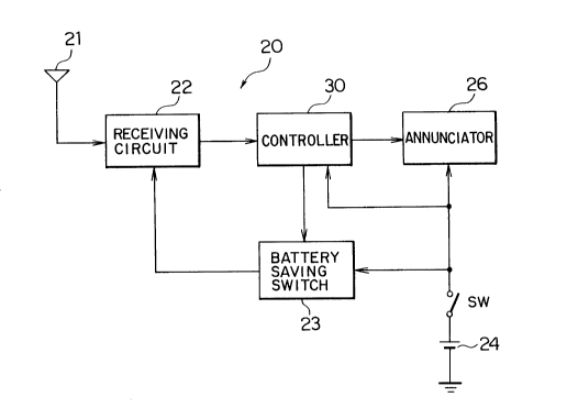
Referring to Fig. 1, a conventional pager
receiver will be described at first in order to
10 facilitate an understanding of the present invention.
According to the prior art, a pager receiver 20
comprises an antenna 21, a receiving circuit 22 for
receiving pager signals through the antenna 21, and a
battery saving switch 23 connected to a battery 24
15 through a power switch SW. The battery saving switch 23
has an on state and an off state. The receiving circuit
22 receives the pager signals as reception pager signals
while the battery saving switch 23 is in the on state.
The receiving circuit 22 supplies the reception pager
20 signals to a controller 25. The controller 25 is
adapted to decide whether or not the reception pager
signa]s contain an address signal which is directed to
the pager receiver 20. Such a decision operation is
called an address decision operation. If the reception
25 pager signals contain the address signal directed to the
pager receiver 20, the controller 25 energizes a speaker
or annunciator 26. The controller 25 serves as a switch
2~3~533
operating circuit for carrying out a battery saving
operation which will shortly be described.
Turning to Fig. 2, the pager signals are
indicated at RS along a top line. Each of the pager
5 signals RS is a POCSAG code signal which is set up in
CCIR recommendation 584. The pager signals RS are
intermittently transmitted by a base station (later
shown). Generally, a time interval T between the pager
signals RS is variable.
Each of the pager signals RS carries a preamble
signal PA and a batch B succeeding the preamble signal
PA. The preamble signal PA has a preamble duration Tp
equal to, for example, an eighteen-code word length when
a unit codeword consists of, for example, 32 bits. The
15 preamble signal PA is specified by a repetition of
pulses which are of logic "l" and "0" levels. The batch
B consists of, for example, seventeen codewords. Other
batches may succeed the illustrated batch B within the
time interval T although only one combination of the
20 preamble signal PA and the batch B is depicted in the
time interval T.
The batch B comprises a frame synchronization
signal SS and first through eighth frames Fl to F8. The
frame synchronization signal SS succeeds the preamble
25 signal PA. The frame synchronization signal SS has a
synchronization duration Ts equal to, for example, a
one-codeword length and is specified by a predetermined
pattern of bits. The first through the eighth frames Fl
2036533
to F8 successively succeed the synchronization signal
SS. Each of first through the eighth frames Fl to F8
has a two codeword length. The first through the eighth
frames Fl to F8 consist of first through eighth call
5 number signals and first through eighth message signals.
The first through the eighth call number signals
are different from each other and may be grouped into
first through eighth groups. The first through eighth
groups are assigned to the first through the eighth
10 frames Fl to F8, respectively. In the top line of Fig.
1, the first call number signal and the first message
signal are symbolized typically at CN and ME,
respectively. Each of the first through the eighth call
number signals and the first through the eighth message
l5 signals has a one-codeword length. The first through
the eighth frames Fl to F8 will collectively be called
an address signal which is depicted at AS. The address
signal AS has an address signal end and an address
duration ending at the address signal end.
As illustrated along a second line, the preamble
signal PA has a preamble duration depicted at Tp. The
synchronization and the address signals SS and AS have a
synchronization duration and an address duration
depicted at Ts and Ta, respectively. A sum of the
25 preamble, the synchronization, and the address durations
is shorter than the time interval T.
Turning back to Fig. 1 and referring to a third
and a fourth or bottom line of Fig. 2, the controller 25
20 3~ 3
16
puts the battery saving switch 23 in the on state during
a first time duration Dl in a time period Tt and
repeatedly at the time period Tt to make the receiving
circuit 22 receive at least a portion of the preamble
5 signal PA. In such an operation, the controller 25
carries out detection of the preamble signal PA. The
operation is called a sampling operation. On detection
of the portion of the preamble signal PA, the controller
25 keeps the on state of the battery saving switch 23
10 until detection of the address signal end. On detection
of the address signal end, the controller 25 puts the
battery saving switch 23 in the off state and then
returns to the sampling operation. Namely, the
controller 25 puts the battery saving switch 23 in the
15 on state repeatedly at the time period Tt to make the
receiving circuit 22 receive a portion of a next one of
the paging signals RS. Thus, the sampling operation is
repeated between the pager signals RS.
Referring to Fig. 3, a pager receiver according
20 to a first embodiment of this invention is similar to
that illustrated in Fig. 1 and comprises similar parts
designated by like reference numerals. A controller 30
carries out the address decision operation in the manner
mentioned above. The controller 30 comprises a read
25 only memory (not shown) memorizing a battery saving
operation program for carrying out the battery saving
operation and comprises a random access memory (not
2036533
shown). The controller 30 carries out time count
operation as will later be described.
Referring to Fig. 4 together with Fig. 3, a
battery saving operation will be summarized. It will be
5 assumed that the pager receiver 20 receives first
through N-th pager signals successively at a first
predetermined time period Tl when the power switch SW is
turned from the off state to the on state. The first
and the second pager signals are indicated at RSl and
10 RS2 along a top line of Fig. 4. The first pager signal
RSl comprises a first preamble signal depicted at PAl, a
first synchronization signal depicted at SSl, and a
first address signal depicted at ASl. Similarly, the
second pager signal RS2 comprises a second preamble
15 signal depicted at PA2, a second synchronization signal
depicted at SS2, and a second address signal depicted at
AS2.
~ s illustrated along a second line of Fig. 4,
each of the first and the second preamble signals PAl
20 and PA2 has the preamble duration Tp. Each of the first
and the second synchronization signals SSl and SS2 has
the synchronization duration Ts. Let the first and the
second address signals ASl and AS2 consist of a single
batch and two batches, respectively. In this event, the
25 first address signal ASl has a first address duration
Tal and the address signal end depicted by a right-most
vertical line outlining the address signal ASl. The
2~3~
second address signal AS2 has a second address duration
Ta2 equal to twice the first address duration Tal.
As illustrated along a third line of Fig. 4, the
controller 30 carries out sampling operation from a time
5 instant at which the power switch SW is closed. Namely,
the controller 30 puts the battery saving switch 23 in
the on state during the first time duration Dl in a
second predetermined time period T2 and repeatedly at
the second predetermined period T2 to make the receiving
10 circuit 22 receive at least a portion of the first
preamble signal PAl. When the receiving circuit 22
receives at least the portion of the first preamble
signal PAl, the controller 30 can detect the first
pxeamble signal PAl. On detection of the first preamble
15 signal PAl, the controller 30 keeps the battery saving
switch 23 in the on state during a second time duration
and detects the first synchronization signal SSl. The
second time duration is illustrated along a fourth line
of Fig. 4 at D2 and is longer than the synchronization
20 duration Ts. The second time duration may be called a
prescribed duration.
When the first synchronization signal SSl is
detected, the controller 30 keeps the switch 23 in the
on state until detection of the address signal end of
25 the first address signal ASl. On detection of the
address signal end, the controller 30 puts the battery
saving switch 23 in the off state until lapse of a
preselected time duration from detection of the first
2036533
. . .
synchronization signal SSl. The preselected time
duration will be called a third time duration. The
third time duration is illustrated along the fourth line
at D3 and is shorter than the first predetermined time
5 period Tl. More specifically, the third time duration
D3 is represented by an equation given by:
D3 -, Tl - (Tp - Ts/2).
At an end of the third time duration, the
controller 30 puts the battery saving switch 23 in the
10 on state during the first time duration Dl to make the
receiving circuit 22 receive a part of the second
preamble signal PA2. When the controller 30 detects the
second preamble signal PA2, the controller 30 keeps the
on state during the second time duration D2 and detects
15 whether or not the second synchronization signal SS2 is
detected within the second time duration D2. When the
second synchronization signal SS2 is detected within the
second time duration D2, the controller 30 keeps the
switch 23 in the on state until detection of the address
20 signal end of the second address signal AS2. On
detection of the address signal end, the controller 30
puts the battery saving switch 23 in the off state until
lapse of the third time duration D3 from detection of
the second synchronization signal SS2. Thus, useless
25 sampling operation is omitted.
Referring to Fig. 5 together with Figs. 3 and 4,
the description will proceed to the battery saving
operation.
2036533
At a first stage Sl, the battery saving
operation starts when the power switch SW is turned from
the off state to the on state.
At a second stage S2 following the first stage
5 Sl, the controller 30 puts the battery saving switch 23
in the off state during a fourth time duration D4 which
is equal to an algebraic sum of the second predetermined
time period T2 minus the first time duration Dl.
At a third stage S3, the controller 30 puts the
10 battery saving switch 23 in the on state during the
first time duration Dl immediately following the fourth
time duration D4.
At a fourth stage S4, the controller 30 judges
whether or not the first preamble signal PAl is detected
15 within the first time duration Dl. If the first
preamble signal PAl is not detected within the first
time duration Dl, operation turns back to the second
stage S2. When the first preamble signal PAl is
detected within the first time duration Dl, operation
20 proceeds to a fifth stage S5. The second through the
fourth stages S2 to S4 are for puttlng the battery
saving switch 23 in the on state repeatedly at the
second predetermined time period T2 to make the
receiving circuit 22 receive at least the
25 above-mentioned portion of the preamble signal of the
first pager signal and produce a first preamble
detection signal. The second through the fourth stages
S2 to S4 are for carrying out the sampling operation and
2~3~3~
may collectively be called a first partial switch
operating unit.
At the fifth stage S5, the controller 30 keeps
the switch 23 in the on state during the second time
5 duration D2 immediately following the first time
duration Dl.
At a sixth stage S6, the controller 30 decides
whether or not the first synchronization signal SSl is
detected within the second time duration D2. When the
10 first synchronization signal SSl is not detected within
the second time duration D2, operation turns back to the
second stage S2. If the first synchronization signal
SSl is detected within the second time duration D2,
operation proceeds to a seventh stage S7. The fifth and
15 the sixth stages S5 and S6 are for putting the switch 23
in the on state during the second time duration D2 from
production of the first preamble detection signal and
for producing a first synchronization detection signal.
The fifth and the sixth stages S5 and S6 may
20 collectively be called a second partial switch operating
unit.
At the seventh stage S7, the controller 30
starts the time count operation of the third time
duration D3. The seventh stage S7 may be called a
25 timer.
At an eighth stage S8, the controller 30 starts
reception operation of the first address signal ASl.
~0~5~3
At a ninth stage S9, the controller 30
determines whether or not the first address signal ASl
is present. In other words, the controller 30 detects
the address signal end of the first address signal ASl.
5 If the first address signal ASl is present, operation
turns back to the eighth stage S8. When either the
first address signal ASl is absent or the controller 30
detects the address signal end of the first address
signals AS1, the controller 30 puts the switch 23 in the
10 off state. Thus, operation proceeds to a tenth stage
S10. The eighth and the ninth stages S8 and S9 are for
putting the battery saving switch 23 in the on state to
make the receiving circuit 22 receive the address signal
ASl of the first pager signal RSl, detect the address
15 signal end of the first pager signal, and produce a
first end detection signal. The eighth and the ninth
stages S8 and S9 may collectively be called a third
partial switch operating unit.
At the tenth stage S10, the controller 20 keeps
20 the off state of the battery saving switch 23 until an
end of the third time duration D3. The tenth stage S10
is for keeping -the switch 23 in the off state from
reception of the first end detection signal until lapse
of the third time duration T3 which is timed by using
25 the first synchronization detection signal. The tenth
stages S10 may be called a fourth partial switch
operating unit.
2036533
At an eleventh stage Sll, the controller 30 puts
the switch 23 in the on state during the first time
duration Dl immediately following the third time
duration D3.
At a twelfth stage S12, the controller 30
decides whether or not the second preamble signal PA2 is
detected within the first time duration Dl. When the
second preamble signal PA2 is not detected, operation
turns back to the second stage S2. If the second
10 preamble signal PA2 is detected, operation proceeds to a
thirteerlth stage S13. The eleventh and the twelfth
stages Sll and S12 are for putting the switch 23 in the
on state during the first time duration Dl to make the
receiving circuit 22 receive at least a part of the
15 preamble signal of each pager signal of the second
through the N-th pager signals and produce a second
preamble detection signal. The eleventh and the twelfth
stages Sll and S12 may collectively be called a fifth
partial switch operating unit.
At the thirteenth stage S13, the controller 30
keeps the switch 23 in the on state during the second
time duration D2.
At a fourteenth stage S14, the controller 30
decides whether or not the second synchronization signal
25 SS2 is detected within the second time duration D2.
When the second synchronization signal SS2 is detected,
operation turns back to the eighth stage S8. The
thirteenth and the fourteenth stages S13 and S14 are for
2036533
24
putting the switch 23 in the on state during the second
time duration D2 from reception of the second preamble
detection signal to make the receiving circuit 22
receive whole of the synchronization and the address
5 signals of the each pager signal and produce a second
synchronization detection signal and a second end
detection signal. The thirteenth and the fourteenth
stages S13 and S14 may collectively be called a sixth
partial switch operating unit.
At the eighth stage S8, the controller 30 starts
reception operation of the second address signal AS2.
At the ninth stage S9, the controller 30 decides whether
or not the second address signal AS2 is present. If the
first address signal AS2 is present, operation turns
15 back to the eighth stage S8. When the second address
signal AS2 is absent, the controller 30 puts the switch
23 in the off state. Then, operation proceeds again to
the tenth stage S10. The tenth stage S10 is for keeping
the switch 23 in the off state from production of the
20 second end detection signal until lapse of the third
time duration D3 which is timed by using the second
synchronization detection signal. In this stage of
operation, the tenth stage S10 may be referred to afresh
as a seventh partial switch operating unit.
If the second synchronization signal SS2 is not
detected at the fourteenth stage S14, operation turns
back to the second stage S2. At the second stage S2
following the fourteenth stage S14, the controller 30
2036533
puts the switch 23 in the off state during the fourth
time duration D4.
At the third stage S3, the controller 30 puts
the switch 23 in the on state during the first time
5 duration Dl.
At the fourth stage S4, the controller 30 judges
whether or not the third preamble signal is detected
within the first time duration Dl. If the third
preamble signal is not detected within the first time
10 duration Dl, operation turns back to the second stage
S2. When the third preamble signal is detected within
the first time duration Dl, operation proceeds again to
the fifth stage S5. The second through the fourth
stages S2 to S4 are for putting the switch 23 in the on
15 state repeatedly at the second predetermined time period
T2 if no preamble signal is received when the battery
saving switch 23 is put intermittently in the on state
during the first time duration Dl. The second through
the fourth stages S2 to S4 may collectively be referred
20 to anew as an eighth partial switch operating unit.
According to the example being illustrated, the
pager receiver has an excellent battery saving
efficiency because the useless sampling operation is
reduced. It should be noted here that the battery
25 saving efficiency becomes higher in proportion to an
increment of the first predetermined time period Tl.
Furthermore, the battery saving operation is useful when
~03~33
26
a small number of calls is given to the pager receiver
20.
Referring to Fig. 6 together with Fig. 3, the
description will be made as regards another battery
5 saving operation which can detect the synchronization
signal even when no preamble signal is detected. The
other battery saving operation is also useful in a pager
receiver of another type. Such a pager receiver is
disclosed in United States Patent No. 4,837,854 issued
ln to Takashi Oyagi and another and assigned to the instant
assignee.
The other battery saving operation is similar to
that illustrated in Fig. 5 except that a fifteenth
through eighteenth stages S15 to S18 are substituted
15 between the third and the sixth stages S3 and S6 for the
fourth and the fifth stages S4 and S5 and a nineteenth
stage Sl9 added between the ninth and the tenth stages
S9 and S10. In the exampLe being illustrated, the
random access memory has a flag code area (not shown)
20 for memorizing a specific flag code as will shortly be
described.
At the third stage S3, the controller 30 puts
the battery saving switch 23 in the on state during the
first time duration Dl.
At the fifteenth stage S15, the controller 30
decides whether or not the receiving circuit 22 receives
a radio signal which may carry the pager signals. When
the receiving circuit 22 does not receive the radio
2~36533
signal, operation turns back to the second stage S2. If
the receiving circuit 22 receives the radio signal as a
reception radio signal, operation proceeds to a
sixteenth stage Sl6.
At the sixteenth stage S16, the controller 30
judges whether or not the reception radio signal is the
preamble signal. If the reception radio signal is the
preamble signal, operation proceeds to a seventeenth
stage S17. When the reception radio signal is not the
10 preamble signal, operation proceeds to the eighteenth
stage S18.
At the seventeenth stage Sl7, the controller 30
sets a preamble detection code represented by logic "l"
level, as the specific flag code, in the flag code area.
15 Subsequently, operation proceeds to the eighteenth stage
S18.
At the eighteenth stage S18, the controller 30
erases the preamble detection code of the flag code
area.
Then, the sixth through the ninth stages S6 to
S9 are successively carried out as described in
conjunction with Fig. 5.
At the nineteenth stage Sl9, the controller 30
decides whether or not the preamble detection code is
25 set in the flag code area. When the preamble detection
code is not set in the flag code area, operation turns
back to the second stage S2. If the preamble detection
code is set in the flag code area, operation proceeds to
2~h~
28
the tenth stage S10. Thereafter, the tenth through the
fourteenth stages Sl0 to S14 are successively carried
out as described in conjunction with Fig. 5.
Referring to Fig. 7, the description will
5 proceed to a control station which is useful for the
pager receiver described in conjunction with Figs. 3 to
5. In the brief description of the drawing, the control
station is said to be according to the third embodiment
of this invention. The control station comprises a
10 processing unit 40 between a telephone network 41 and a
base station 42. The processing unit 40 is supplied
with call information from the telephone network 41 and
processes the call information into processed signals.
The base station 42 is for successively transmitting the
15 processed signals as the pager signals carried by a
radio signal. The call information may comprise a call
number signal and a message signal. The call number
signa] represents a call number. The message signal
represents a message.
The processing unit 40 comprises an input
section 43 for receiving the call information. A
queuing buffer memory 44 is for memorizing the call
information as memorized information. An information
processor 45 is for processing the memorized information
25 into processed information. A controller 46 is for
controlling the input section 43, the queuing buffer
memory 44, and the information processor 45. The
processing unit 40 further comprises a subscriber file
2036533
29
memory 47 preliminarily memorizing a plurality of
subscriber numbers, and a timer 48 for timing a preamble
duration, a synchronization duration, and an address
including duration successively in a predetermined time
5 period T to produce a time-out signal. The address
including duration is what should be referred to more
exactly as an address signal including duration. The
information processor 45 comprises a signal generating
unit 49 for generating a preamble signal having a first
10 duration and a synchronization signal having a second
duration and a partial processor 50 for processing the
memorized information into address signals. Each of the
address signals has a variable duration as an address
duration which immediately follows the synchronization
lS duration and is shorter than the address including
duration. The first and the second durations are equal
to the preamble and the synchronization durations
described in conjunction with Fig. 2, respectively.
The queuing buffer memory 44 comprises first
20 through third queuing memory areas QMl, QM2, and QM3 and
a transferring memory area TM. Each of the first
through the third queuing memory areas QMl to QM3 and
the transferring memory area TM has a memory capacity
capable of memorizing a maximum number of batches which
25 can be produced within the first predetermined time
period Tl. The queuing buffer memory 44 further
comprises a flag memory area (not shown) for memorizing
a flag code for indicating whether the queuing buffer
2036~33
memory 44 is full or vacant. The flag code is set in a
busy state by a logic "li' level when all of the first
through the third queuing memory areas QMl to QM3 and
the transferring memory area TM are full.
Referring to Fig. 8 together with Fig. 7, the
description will proceed to reception operation of the
call information. The reception operation is carried
out by the controller 46 in cooperation with the input
section 43 and the queuing buffer memory 44.
At a first stage STl of the reception operation,
the controller 46 detects whether or not the flag code
indicates the busy state. When the flag code indicates
the busy state, the first stage STl is repeated. If the
flag code does not indicate the busy state but the
15 vacant state, operation proceeds to a second stage ST2.
At the second stage ST2, the controller 46
detects whether or not a call is represented by the call
information. When the call is present, operation turns
back to the first stage STl. If the call is absent,
20 operation proceeds to a third stage ST3.
At the third stage ST3, the input section 43
receives the call information as reception call
information.
At a fourth stage ST4, the controller 46
25 receives the call number of the reception call
information as a received call number and decides
whether or not the received call number is memorized in
the subscriber file memory 47. When the received call
31 2036533
number is not memorized in the subscriber file memory
47, operation proceeds to a fifth stage ST5. If the
received call number is memorized in the subscriber file
memory 47, operation proceeds to a sixth stage ST6.
At the fifth stage ST5, the controller 46
controls the input section 43 to make the input section
43 supply an invalid tone signal back to the telephone
network 41. As well known in the art, the invalid tone
signal is for informing that the call is invalid.
10 Supplied with the invalid tone signal, the telephone
network 41 delivers an invalid tone to a subscriber (not
shown~ in the manner known in the art. Subsequently,
operation turns back to the first stage STl. This means
that the call is rejected.
At the sixth stage ST6, the controller 46
receives the message signal of the call information as a
received message signal.
At a seventh stage ST7, the controller 46
decides whether or not the first queuing memory area QMl
20 has a vacant area. If the first queuing memory area QMl
has the vacant area, operation proceeds to an eighth
stage ST8. When the first queuing memory area QMl has
no vacant area, namely, the first queuing memory area
QMl is full, operation proceeds to a ninth stage ST9.
At the eighth stage ST8, the controller 46
stores the received call number and the received message
signal in the first queuing memory area QMl.
2036533
32
Suhsequently, operation turns back to the first stage
ST1.
At the ninth stage ST9, the controller 46
decides whether or not the second queuing memory area
5 QM2 has a vacant area. If the second queuing memory
area QM2 has the vacant area, operation proceeds to a
tenth stage ST10. When the second queuing memory area
QM2 has no vacant area, operation proceeds to an
eleventh stage STll. When the second queuing memory
10 area ~M2 is full, the control statlon may be regarded as
being in a congestion state of calls. In this event, if
the controller 46 accepts a new call, the control
station falls into a degraded service. Accordingly, the
new call should be rejected as will shortly be
15 descrihed.
At the tenth stage ST10, the controller 46
stores the received call number and the received message
signal in the second queuing memory area QM2.
Subsequently, operation turns back to the first stage
20 STl.
At the eleventh stage STll, the controller 46
sets the flag code in the busy state. As a result, the
new call is rejected at the first stage STl.
At a twelfth stage ST12, the controller 46
25 decides whether or not the third queuing memory area QM3
has a vacant area. If the third queuing memory area QM3
has the vacant area, operation proceeds to a thirteenth
stage ST13. When the third queuing memory area QM3 has
2U36533
no vacant area, operation proceeds to a fourteenth stage
STl4.
At the thirteenth stage STl3, the controller 46
stores the received call number and the received message
5 signal into the third queuing memory area QM3.
Subsequently, operation turns back to the first stage
STl.
At the fourteenth stage STl4, the controller 46
controls the input section 43 to make the input section
10 43 supply the invalid tone signal to the telephone
network 41 as mentioned before. In this event, the call
is rejected. Then, operation turns back to the first
stage STl.
Turning to Fig. 9 with reference to Fig. 7
15 continued, the description will proceed to output
operation of the processed signal. The output operation
is carried out by the controller 46 in cooperation with
the queuing buffer memory 44, the information processor
45 and the timer 48. Let each of the first through the
20 third queuing memory areas QMl to QM3 already memorize
first through third memorized information, respectively.
Similarly, the transferring memory area TM already
memorizes a fourth memorized information.
At a first stage SSl of the output operation,
25 the controller 45 detects whether or not the timer 48
produces the time-out signal. When the timer 48 does
not yet produce the time-out signal, the first stage SSl
2o36533
34
is repeated. If the timer 48 produces the time-out
signal, operation proceeds to a second stage SS2.
At the second stage SS2, the controller 46
shifts the first memorized information from the first
5 queuing memory area QMl to the transferring memory area
TM and shifts the fourth memorized information from the
transferring memory area TM back to the third queuing
memory area QM3. Similarly, the controller 46 shifts
the third memorized information f~om the third queuing
10 memory area QM3 to the second queuing memory area QM2
and the second memorized information from the second
queuing memory area QM2 to the first queuing memory area
QMl. As a result, the first through the third queuing
memory areas QMl to QM3 memorize the fourth, the third,
15 and the second memorized information as first through
third shifted information, respectively. Similarly, the
transferring memory area TM memorizes the first
memorized information as fourth shifted information.
At a third stage SS3, the controller 46 decides
20 whether or not the transferring memory area TM memorizes
at least one of the call number and the message signal.
If the transferring memory area TM memorizes the fourth
shifted information comprising one of the call number
and the message signal, operation proceeds to a fourth
25 stage SS4. When the transferring memory area TM
memorizes none of the call number and the message
signal, operation proceeds to a fifth stage SS5. The
third stage SS3 is for detecting repeatedly at the
2~36533
predetermined period T whether or not the call
information is memorized in the transferring memory area
TM to produce an empty detection signal while the
transferring memory area TM memorizes none of the call
5 number and the message signal. Therefore, the third
stage SS3 may be called a detecting unit.
At the fourth stage SS4, the queuing buffer
memory 44 transfers the fourth shifted information from
the transferring memory area TM to the partial processor
10 50. Supplied with the fourth shifted information, the
partial processor 50 processes the fourth shifted
information into one of the address signals.
Simultaneously, the partial processor 50 is supplied
with the preamble and the synchronization signals from
15 the signal generating unit 49. The controller 46
controls the partial processor 50 to make the partial
processor 50 consecutively transmit the preamble and the
synchronization signals and one of the address signals
to the base station 42 in the preamble, the
20 synchronization, and the address including durations
collectively as one of the processed signals.
At a sixth stage SS6, the controller 46 erases
the fourth shifted information memorized in the
transferring memory area TM.
At a seventh stage SS7, the controller 46 resets
the busy state in the flag memory area. Subsequently,
operation turns back to the first stage SSl.
36 2036533
At the fifth stage SS5, the signal generating
unit 49 supplies the preamble and the synchronization
signals to the partial processor 50.
At an eighth stage SS8, the controller 46
5 controls the partial processor 50 to make the partial
processor 50 consecutively transmit, during presence of
the empty detection signal, the preamble signal, the
synchronization signal, and no signal to the base
station 42 in the preamble, the synchronization, and the
10 address including durations collectively as a dummy
signal rather than as one of the processed signals. The
dummy signal will later be taken into account. Then,
operation turns back to the first stage SSl. The eighth
stage SS8 may be called a partial control unit.
In the manner mentioned above, the control
station can produce the processed signals at the first
predetermined time period Tl regardless of the
congestion state of calls. Furthermore, the control
station can produce the processed signals successively
20 at the first predetermined time period Tl without
interruption even when the control station is supplied
with no call information.
Referring to Fig. 10, a pager receiver is
similar in structure to the pager receiver illustrated
25 in Fig. 3. In the brief description of the drawing, the
pager receiver is said to be according to the second
embodiment of this invention. The controller 30
operates in a following manner.
2036533
As illustrated along a top line of Fig. 10, let
the pager receiver receive first through (L-l)-th and
L-th through N-th pager signals successively at a
predetermined time period T, where (L - 1) represents a
5 first integer which is less than about ten, (N - L)
representing a second integer which is not less than
one. Let each of the first through the N-th pager
signals comprise the preamble signal PA having the
preamble duration and the batch B which is described
10 above. The batch B comprises the synchronization signal
SS succeeding the preamble signal PA and having the
synchronization duration and the address signal AS
succeeding the synchronization signal SS and having the
address signal end and the address duration ending at
15 the address duration. A sum of the preamble, the
synchronization, and the address durations is not longer
than the predetermined time period T.
Referring to Fig. 11 together with Figs. 3 and
10, the description will be made as regards the battery
20 saving operation.
At a first stage SPl of this battery saving
operation, the power switch SW is turned from the off
state to the on state.
At a second stage SP2, preparing operation is
25 carried out as will later be described more in detail.
In short, the preparing operation is for determining the
predetermined time period T to prepare the receiving
circuit 22 for its operation by putting the battery
2036~33
38
saving switch 23 in the on state to make the receiving
circuit 22 receive the synchronization signals of the
first through the (L~ th pager signals as received
signals and detect the address signal end of the
5 (L~ th pager signal and to use the received signals in
determining the predetermined time period T.
At a third stage SP3, the controller 30 starts
time count operation of a first time interval from
reception of the synchronization signal of the (L-l)-th
10 pager signal. The first time interval is depicted at
tOl along a second line of Fig. 9.
At a fourth stage SP4, the controller 30 decides
whether or not the address signal of the (L-l)-th pager
signal is present. In other words, the controller 30
15 detects the address signal end of the (L-l)-th pager
signal. If the address signal is present, the fourth
stage SP4 is repeated. When either the address signal
is absent or the controller 30 detects the address
signal end of the (L-l)-th pager signal, operation
20 proceeds to a fifth stage SP5.
At the fifth stage SP5, the controller 30 puts
the battery saving switch 23 in the off state.
At a sixth stage SP6, the controller 30 decides
whether or not the first time interval tOl is over.
25 When the first time interval tO1 does not elapse, the
sixth stage SP6 is repeated. If the first time interval
tOl is over, operation proceeds to a seventh stage SP7.
2036533
39
At the seventh stage SP7, the controller 30 puts
the switch 23 in the on state and starts time count
operation of a second time interval. The second time
interval is depicted at tO2 along the second line of
5 Fig. 10. The second time interval tO2 is, for example,
0.125 second long. The first time interval tOl is equal
to an algebraic sum of the predetermined period T minus
the second time interval tO2. The second time interval
tO2 is longer than the synchronization duration and
10 shorter than twice the synchronization duration.
At an eighth stage SP8, the controller 30 decides
whether or not the second time interval tO2 is over. If
the second time interval tO2 is over, operation turns
back to the second stage SP2. When the second time
15 interval does not elapse, operation proceeds to a ninth
stage SP9.
At the ninth stage SP9, the controller 30
decides whether or not the receiving circuit 22 receives
the synchronization signal of the L-th pager signal
20 within the second time interval tO2. When the receiving
circuit 22 does not receive the synchronization signal
of the L-th pager signal within the second time
interval, operation turns back to the eighth stage SP8.
When the receiving circuit 22 receives the
25 synchronization signal, operation turns back to the
third stage SP3.
As is obvious from the above, the third through
the ninth stages SP3 to SP9 are for carrying out the
2036533
battery saving operation. In the battery saving
operation, the battery saving switch 23 is put in the on
state during the second time interval tO2 immediately
following the first time interval tOl to make the
5 receiving circuit 22 receive the synchronization and the
address signals of each signal of the L-th through the
N-th pager signals and detect the address signal end of
the each signal. Furthermore, the battery saving switch
23 is put in the off state from detection of the address
10 signal end of the each signal until lapse of the first
time interval tO2 from reception of the synchronization
signal of the each signal. The third through the ninth
stages SP3 to SP9 may collectively be called a switch
operating unit.
Turning to Fig. 12, the description will proceed
to the preparing operation for determining the
predetermined time period T. In the preparing
operation, the controller 30 repeats period determining
operation (L - 2) times by detecting the synchronization
20 signal of the first through the (L-l)-th pager signals.
In short, the predetermined period T is determined by
detecting an interval between one of the synchronization
signal and a next one of the synchronization signal.
Therefore, the period determining operation starts from
25 reception of the synchronization signal of the second
pager signal. The controller 30 counts the number of
the period determining operation as a counted value.
~036533
41
At a first stage SGl of the preparing operation,
the controller 30 starts the period determining
operation.
At a second stage SG2, the controller 30 sets
5 the counted value at zero.
At a third stage SG3, the controller 30 decides
whether or not the preamble signal of the second pager
signal is received. When the preamble signal is not
received, the third stage SG3 is repeated. If the
10 preamble signal is received, operation proceeds to a
fourth sta~e SG4.
At the fourth stage SG4, the controller 30
decides whether or not the synchronization signal of the
second pager signal is received. When the
15 synchronization signal is not received, operation turns
back to the second stage SG2. If the synchronization
signal is received, operation proceeds to a fifth stage
SG5.
At the fifth stage SG5, the controller 30
20 determines the predetermined period T, as a first
determined period, by detecting the interval between the
synchronization signals of the first and the second
pager signals. The controller 30 stores the first
determined period in the random access memory mentioned
25 before. Simultaneously, the controller 30 counts up the
counted value to one.
At a sixth stage SG6, the controller 30 decides
whether or not the counted value is equal to one. When
2036533
42
the counted value is not equal to one, operation
proceeds to a seventh stage SG7. If the counted value
is equal to one, operation proceeds to an eighth stage
SG8. At this moment, operation proceeds to the eighth
5 stage SG8 because the counted value is equal to one.
At the eighth stage SG8, the controller 30
decides whether or not the address signal of the second
pager signal is present. If the address signal is
present, the eighth stage SG8 is repeated. When the
10 address signal is absent, operation turns back to the
third stage SG3.
At the third stage SG3, the controller 30
decides whether or not the preamble signal of the third
pager signal is received. When the preamble signal is
15 not received, the third stage SG3 is repeated. If the
preamble signal is received, operation proceeds to the
fourth stage SG4.
At the fourth stage SG4, the controller 30
decides whether or not the synchronization signal of the
20 third pager signal is received. When the
synchronization signal is not received, operation turns
back to the second stage SG2. If the synchronization
signal is received, operation proceeds to the fifth
stage SG5.
At the fifth stage SG5, the controller 30
determines the predetermined period T, as a second
determined period, by detecting the interval between the
synchronization signals of the second and the third
2~36533
43
pager signals. The controller 30 stores the second
determined period in the random access memory.
Simultaneously, the controller 30 changes the counted
value to two.
At the sixth stage SG6, the controller 30
decides whether or not the counted value is equal to
one. When the counted value is not equal to one,
operation proceeds to the seventh stage SG7. If the
counted value is equal to one, operation proceeds to the
10 eighth stage SG8. At this moment, operation proceeds to
the seventh stage SG7 because the counted value is equal
to two.
At the seventh stage SG7 r the controller 30
calculates a first difference between the first and the
15 second determined periods.
At a ninth stage SG9, the controller 30 decides
whether or not the first difference is less than a
predetermined value. When the first difference is less
than the predetermined value r operation proceeds to a
20 tenth stage SG10. If the first difference is not less
than the predetermined value, operation proceeds to an
eleventh stage SGll.
At the eleventh stage SGll r the controller 30
stores the second determined period in the random access
25 memory as a previously determined period. This means
that the second determined period is stored in the
random access memory in place of the first determined
period. Simultaneouslyr the controller 30 changes the
2036533
counted value to three. Then, operation proceeds to the
eighth stage SG8.
At the tenth stage SGlO, the controller 30
decides whether or not the period determining operation
5 is repeated (L - 1) times. When the number of the
period determining operation does not reach the (L - 1)
times, operation proceeds to the eleventh stage SGll.
If the period determining operation is repeated the
(L - 1) times, operation proceeds to a twelfth stage
10 SG12.
At the twelfth stage SG12, the controller 30
calculates an arithmetic mean value of the first through
an (L - l)-th determined periods.
At a thirteenth stage SG13, the preparing
15 operation comes to an end.
Referring to Figs. 13 and 14, the description
will be made as regards a control station according to a
fourth embodiment of this invention. The control
station is useful for the pager receiver 20 described in
20 conjunction with Figs. 10 to 12. The control station 60
comprises an active and a backup control units 61 and 62
each of which is similar in structure and operation to
each other. The control station 60 further comprises an
active and a backup processing circuits 63 and 64. Each
25 of the active and the backup processing circuits 63 and
64 is similar in structure and operation to each other.
Each of the active and the backup control units 61 and
62 is connected to a telephone network 65 through a
2036533
plurality of input trunks 66 and supplied with the call
information from the telephone network 65. The control
units 61 and 62 may collectively be called a control
unit depending on the circumstances.
Each of the active and the backup processing
circuits 63 and 64 is connected to first through M-th
output trunks 67-1 to 67-M. The first through the M-th
output trunks 67-1 to 67-M are connected to first
through M-th base stations 68-1 to 68-M, respectively,
10 which have first through M-th service areas 69-1 to
69-M, respectively. Each of the active and the backup
processing circuits 63 and 64 is for processing the call
information into processed signals successively at the
predetermined time period T to make the first through
15 the M-th base stations 68-1 to 68-M transmit the
processed signals as the pager signals.
The control station further comprises a signal
generating unit 71 for generating an instruction signal.
In Fig. 13, the instruction signal is indicated
20 at IS along a first line. As will later be described,
the instruction signal is for putting a selected one of
the active and the backup processing circuits 63 and 64
into operation. For example, when the instruction
signal is present, the active control unit 61 puts the
25 active processing circuit 63 into operation of producing
the processed signals while the backup control unit 62
puts the active processing circuit 64 out of operation
of producing the processed signals. On the contrary,
- 2036533
46
when the instruction signal is absent, the active
control unit 61 puts the active processing circuit 63
out of operation of producing the processed signals
while the backup control unit 62 puts the active
5 processing circuit 64 into operation of producing the
processed signals. It should be noted here that the
predetermined time period T repeatedly follows one after
another as a succession of predetermined time periods.
As illustrated at a left-hand part along a second line,
10 the active processing circuit 63 is put into operation
upon start of one of the predetermined periods that
starts in the succession earliest after appearance of
the instruc-tion signal IS. As illustrated at a
right-hand part of the second line, the backup
15 processing circuit 64 is put into operation upon start
of one of the predetermined periods that start in the
succession earliest after disappearance of the
instruction signal IS.
For brevity, the description will be made only
20 as regards the active backup control unit 61 and the
active processing circuit 63. When supplied with the
call information, the active backup control unit 61
carries out collation operation, such as a subscriber
collation and a service menu collation, in the manner
25 known in the art. After the collation operation, the
active ~ackup control unit 61 supp-lies the call
information to the active processing circuit 63 and
controls the active processing circuit 63. Supplied
203~533
47
with the call information, the active processing circuit
63 processes the call information into processed signals
in the manner described in conjunction with Fig. 7. The
processing circuit 63 delivers the processed signals
5 successively at the predetermined time period T to the
first through the M-th base stations 68-1 to 68-M
through the first through the M-th output trunks 67-1 to
57-M. The first through the M-th base stations 68-1 to
,
68-M transmit the processed signals as the pager signals
10 through first through M-th transmitting antennas 70-1 to
70-M, respectively.
The control station 60 further comprises a
change signal generating unit 72 for generating a change
indication signal. The control station 60 further
15 comprises a timer 73 for timing the predetermined time
period T to make each of the active and the backup
control units 61 and 62 put each of the active and the
backup processing circuits 63 and 64 into operation at
the predetermined period T. The timer 73 changes the
20 predetermined time period T to a prescribed time period
T' when supplied with the change indication signal.
From disappearance of the change indication signal, each
of the active and the backup control units 61 and 62
puts the active and the backup processing circuits 63
25 and 64 into operation of producing the processed signals
successively at the prescribed time period T' when the
prescribed time period T' starts earliest from
disappearance of the change indication signal. It
2036533
48
should be noted here that the predetermined period
repeated]y follows one after another as a succession of
predetermined time periods. Each of the active and the
backup processing circuits 63 and 64 is put into
5 operation upon start of one of the predetermined periods
that starts in the succession earliest after
disappearance of the change indication signal. The
prescribed time period T' should be longer than the
second timer interval tO2 to make the pager receiver
10 detect the synchronization signal as described in
conjunction with Figs. 10 and 11. The timer 73 may
count a time period longer than the predetermined time
period T in place of the predetermined time period T.
Referring to Fig. 14 together with Fig. 13, the
15 description will be directed to control operation of the
active and the backup control units 61 and 62.
At a first stage SEl of the control operation,
let the signal generating unit 71 stop generation of the
instruction signal IS. In this event, the control
20 operation is changed from the active control unit 61 to
the backup control unit 62.
At a second stage SE2, the backup control unit
62 decides whether or not the control operation is
operable. When the control operation is not operable,
25 the second stage SE2 is repeated. If the control
operation is operable, operation proceeds to a third
stage SE3.
2036533
49
At the third stage SE3, the backup control unit
62 resets operation of the backup processing circuit 64
and resets the timer 73.
At a fourth stage SE4, the backup control unit
5 62 decides whether or not the timer 73 counts up the
predetermined time period T. If the timer 73 does not
count up the predetermined time period T, the fourth
stage SE4 is repeated. When the timer 73 counts up the
predetermined time period T, operation proceeds to a
10 fifth stage SE5.
At the fifth stage SE5, the backup control unit
62 decides whether or not the change indication signal
is generated. When the change indication signal is
generated, operation proceeds to a sixth stage SE6. If
15 the change indication signal is not generated, operation
proceeds to a seventh stage SE7.
At the seventh stage SE7, the backup control
unit 62 again resets the timer 73.
At an eighth stage SE8, the backup control unit
20 62 controls the backup processing circuit 64 to make the
backup processing circuit 64 produce one of the
processed signals. Then, operation turns back to the
fourth stage SE4. Thereafter, the fourth through the
eighth stages SE4 to SE8 are repeated.
At the sixth stage SE6, the timer 73 changes the
predetermined time period T to the prescribed time
period T'.
2036533
At a ninth stage SE9, the baekup eontrol unit 62
deeides whether or not the timer 73 eounts up the
preseribed time period T'. If the timer 73 does not
count up the prescribed timer period T', the ninth stage
5 SE9 is repeated. When the timer 73 eounts up the
prescribed time period T', operation proeeeds again to
the seventh stage SE7.
At the seventh stage SE7, the baekup eontrol
unit 64 resets the timer 73.
At the eighth stage SE8, the baekup eontrol unit
62 controls the backup processing circuit 64 to make the
backup processing circuit 64 produce one of the
processed signals. Then, operation turns back to the
fourth stage SE4. Thereafter, the fourth through the
15 eighth stages SE4 to SE8 are repeated.
According to the above-described control
operation, the-pager signals can be received eorreetly
by the pager receiver described in conjunetion with
Figs. 10 and 11. In other words, the pager reeeiver ean
20 receive the pager signals without error even when one of
the active and the backup processing circuits 63 and 64
is changed to another one of the active and the backup
proeessing eireuits 63 and 64 and even when the timer 73
changes one of the predetermined and the prescribed time
25 periods T and T' to another one of the predetermined and
the prescribed time periods T and T'. When the timer 73
defines the prescribed timer period T', the pager
receiver 20 should be put into operation with the
51 2036533
prescribed period T' used either as the first
predetermined time period T1 or as the predetermined
time period T.
While this invention has thus far been described
5 in conjunction with a few embodiments thereof, it will
readily be possible for those skilled in the art to put
this invention into practice in various other manners.
For example, the timer 48 may be included in the
controller 46. Similarly, the timer 73 may be included
lO in the active and the backup control units 61 and 62.