Note: Descriptions are shown in the official language in which they were submitted.
203~957
. SEMICONDUCTOR LASER DIODE ARRANGEMENT
TECHNICAL FIELD
The invention concerns ~a laser diode arrangement with an epitaxially grown
layered semiconductor structure in which an array of laser diodes and a plurality
of integrated reflectors, one for each beam emitted by the array, are formed. The
reflectors create an array of virtual sources with lateral distances the~ebel~ ~,tn
that differ from the physical spacing of the laser diodes. More particularly, the
virtual sources may be more closely spaced than the laser diodes and can even
be concentrated in a single spot. A single lens can be used to project the array of
virtual sources.
BACKGROUND OF THE INVENTION
Semiconductor laser diodes have found applications in a wide variety of
information handling systems because of their compact slze and because their
technology is compatible with that of associated electronic circuitry and other
electro-optical elements like, e.g., mirrors. They are being used in areas such as
data communication, optical storage and optical beam printing.
Efforts aiming at improved performance in applications requiring more than
one light source have led to the design of integrated laser arrays capable of
emitting a plurality of closely spaced laser beams. In general, they are employed
to replace slower serial operations by faster parallel processing,. e.g.,
, ~ I
203~9S7
2 SZ 9-89-017
byte-processing instead of bit-by-bit processing, or in document scanning and
printing.
-
"~ A wide variety of laser array structures have been described, some of the
publications being listed here:
-- Article"Experimental and Analytic Studies of Coupled Multiple Stripe DiodeLasers" by D.R.Scifres et al (IEEE Journal of Quantum Electronics, Vol.QE-15,
No.9, September 1979, pp 917-922).
-- U.S. Patent 4,069,463 "Injection Laser Array" (issued January 1978).
-- Europeam Patent Application 0 226 445, "Laser Array" (published June 24,
1987) .
-- European Patent Application 0 301 818, "Semiconductor Laser Array Device"
(published February 1, 1989).
-- European Patent Application 0 301 846, "Semiconductor Laser Array
Apparatus" (published February 1, 1989).
Despite the progress made in recent years in developing prucesses to
minimize device dimensions, a further reduction in the spacing between
individual beams is still highly desirable for a number of high resolution
applications. One approach that has been pursued is the use of optical systems
to bring the laser beams closer together. However, the use of individual lens
systems for each beam make such arrangements prohibitively complex and
expensive and, in addition, for devices requiring feature dimensions in the order
of microns, optical systems are at their physical limits. The laser arrangement
described herein below points in a new direction.
Besides the efforts to arrive at closely spaced beams, there have been
developments aiming at the design of surface emitting lasers wherein beams
emitted in a plane parallel to the wafer surface on which the laser structure isepitaxially grown, are reflected at an integrated mirror to exit the device
perpendicular to the wafer surface, mainly in order to facilitate packaging. Such
arrangements have, e.g., been disclosed in
~ 2~369 ~;,9~9(~17
-- U.S.Patent 3,996,492, "Two-Dimensional Integrated Inlectlon Laser Array"
(issued December 7, 1976) .
-- U.S.Patent 3,996,528, "Folded Cavity InJection Laser" (issued December 7,
1976).
- U.S. Patent 4,901,329, "Integrated Laser Arrays and Support
Circuits" (issued February 13, 1990) and U.S. Patent 4,971,927,
"Integrated Laser Arrays and Support Circuits" (issued November
20, 1990)
-- IBM Technlcal Disclosure Bulletin, Article "Vertically Emitting Laser with
Integrated NAM Deflector" (Vol. 32, No.3B, August 1989, pp 498 - 499).
Another approach to obtaln surface emitting laser diodes is described in an
Artlcle "Surface Emitting Laser Diode with bent Waveguide", by M.Ogura et al
(Appl. Phys. Lett. 50(12), 23 March 1987, pp 705 - 707). There, a bent double
heterostructure fabricated on a grooved substrate is used instead of a deflecting
mirror.
- llowever, to our knowledge, no suggestion has yet been made to make use of
the optical elements, required to achieve the desired "surface emitting", to
provide virtual sources that are closer spaced than the corresponding beam
sources and that can be proJected using simple optical means.
With regard to the optical prlnciple on which the herein described laser diode
arrangement is based, there exists some similarity with the so-called "Fresnel's
mirror" arrangement where light from a point source is incident on two plane
mirrors mutually inclined at a small angle. Reflection at the mirrors gives ralse to
two virtual images. A description can be found in the handbook "Principles of
Optics", Max Born & Emil Wolf, Pergamon Press, 6th Edition, p.262. This
, ,fe, t:nce, however, does not in any way suggest any potential technical
application of the described optical principle.
B~
2036957
4 sZ 9-89-0 1 7
SUMMARY OF THE INVENTION
~- It is the main object of the present invention to provide a laser diode
arrangement in which a plurality of laser beam sources is transfered into a
contracted or even coincident collection of virtual sources that can be projected
onto a desired processing plane using simple optical means.
Another object is to provide a "surface emitting" integrated laser array
structure from which the emitted laser beams exit in a direction essentially
perpendicular to the surface of the wafer on which the structure is formed.
A further main object is to provide a method allowing the fabrication of the
proposed integrated, surface emitting, reduced beam separation laser diode
arrangement using a conventional unidirectional process in connection with
proper masking segment geometries.
The invention as claimed is intended to meet these objectives and to remedy
the deficiencies of known laser diode arrangements. In the inventive structure
this is accomplished in that, for each of a plurality of laser beams emitted from a
laser array, an individually oriented and positioned reflector is provided. These
reflectors produce an array of virtual sources, the dlstances between these
virtual sources being different from the distances between the corresponding
beams (or real sources). Using a single lens, the array of virtual sources Is then
projected onto a desired plane. Most important will be embodiments in which the
virtual sources are brought closer together or where they even coincide.
The group of required reflectors, one for each beam, can be fabricated in a
single directional dry-etch process using a mask whose segments (together with
the common angle of the directional etch) properly determine the individual
positions and lhe orientations of the tilted reflecting surfaces.
The main advantage offered by the invention is that the proposed structure
can serve as a device transfering a plurality of laser beam sources into closer
spaced, contracted laser sources which may even coincide. A few examples of
2036957
SZ 9-89-017
applications where the inventive laser diode arrangment may be advantageously
used are:
Band-recording when spacing between tracks is smaller than the smallest
obtainable spacing between adjacent lasers in a laser array: contracted virtual
sources allow parallel recording on adjacent tracks.
Gradual laser degradation depends on laser power; it can be reduced by
operating several lasers with coincident virtual sources at a fractional power.
Laser reliability may be vastly improved through redundancy; this can be
obtained with coincident virtual sources, employed either sequentially or in
combination.
Power density in an imaged spot obtainable with a single laser diode is
limited mainly because of catastrophic failure at the laser mirrors; the limit
can be raised using coincident virtual sources.
Short coherence length is important in some communica~ions applications;
this length can be shortened by combining the outputs of coincident virtual
sources.
DESCRIPTION OF THE DRAWINGS
One way of implementing the invention is described in detail below with
reference to drawings which illustrate a specific embodiment and in which
Fig. 1 is a schematic view of a state of the art integrated "surface
emitting" laser diode/reflector structure. (PRIOR ART).
i ig. 2 is a schematic illustration of the main elements of the inventive
diode laser arrangement (used to explain the underlying
concept) .
:
20369~7
6 SZ 9-89-017
Fig. 3 is a schematic illustration of the principle of the laser
array/reflector arrangement and the key process parameters for
the fabrication of the required individual reflectors.
Fig. 4 shows, schematically and largely simplified, top views of
(A,B & C) diflerent reflector arrangements.
Flg. 5 is a perspective view of an embodiment of an integrated laser
array/reflector arrangement designed in accordance with the
prese~nt invention.
DETAILED DESCRIPTION
Before describing an embodiment of the inventive laser diode array in
greater detail, the tilted reflector concept, applied in the structure to arrive at
a surface emitting laser device, will be outlined with the aid of Fig.1.
Fig.1 is a perspective view of a known surface emitting laser structure 10 of
which only the main elements are shown. These are the laser diode 11 and
the integrated 45 reflector 12. Both are formed in a stack of layers that are
epitaxially grown on a GaAs substrate 13, the stack including at least the
active layer 14 sandwiched between cladding layers. For simplicity reasons,
only the active layer is indicated in the figure. The drawing shows the
structure after completion of the etch process forming the groove 15 that
provides the laser mirror facet 16 and the 45 reflecting surface 17. Omitted
in the drawing are the metallization layers providing for the elctrical contactsto the completed device.
When the device is activated by applying proper operating voltages, a light
beam 19 A is emitted. In the drawing, the llght mode region of the laser is
shown as a small ellipse centering around the active layer 14 and laterally
defined by the stripe ridge 18. Arrow 19 represents the "real" source of the
emitted beam 19 A which impinges onto the 45 surface 17. Here it is
20369~7
7 SZ 9-89-017
deflected making the laser "surface emitting", i.e., the output beam 19 B is in
a direction essentially perpendicular to the substrate surface. Beam 19 B can
be consTdered as being emitted without deflection from a virtual source 19'.
The purpose of the invention is to apply the tilted reflector concept to an
- array of integrated lasers and to simultaneously reduce the separation
between the individual lasers of the array to an apparent (or virtual) smaller
spacing thereby meeting the demand for multiple beam sources with spacings
between the sources smaller than the smallest separation at which lasers can
be fabricated and operated. The invention allows to transform a collection of
real sources into a contracted or even coincident collection of virtual sources
which can than be projected, using a single lens, to provide the required
reduced-scale light pattern.
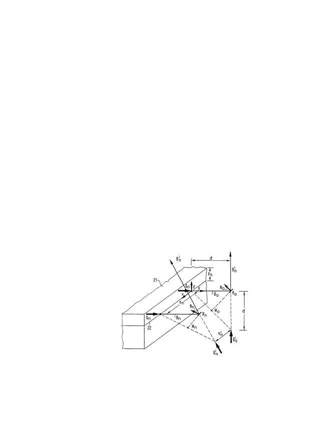
The principle will now be described with reference to figures 2 and 3. Fig.2
schematically illustrates a laser array structure 21 (similar in structure to the
laser 11 of Fig.1), with two light sources QO and Qn~ emitting beams Bo and Bn~
respectively. These "real" sources are formed by respective waveguides along
the y-direction, the front mirror facets being in the x-z plane. It is, however,noted that, conceptually, the front mirrors do not have to be co-planar.
Beam Bo~ proceeding in the y-z plane, is reflected at reflector Ro and
projected upwardly. The reflector surface is tilted 45, its "normal"
(perpendicular to the reflecting surface) is shown as arrow No . The virtual
source QO' Of the beam is at the position indicated in the drawing.
The second source Qn, representing any other source in the array, emits a
beam Bn from the array at a point that is separated from QO by a distance Sn~
Its beam Bn is intersected by the reflector Rn
The position of the respective virtual source Qn' is determined by the
orientation and position of the reflector Rn . As explained above, it is the goal
to achieve a virtual source Qn' located at a distance s,~' from QO ~ that is
different from the separation Sn Of the respective real sources QO and Qn. In
~::
203~957
8 SZ 9-89-0 17
the extreme case, Sn~ = O, i.e., the virtual sources coincide and the respectiveseparated real sources are projected onto a single spot.
The requirements and conditions for properly orienting and positioning any
reflector Rn are now developed. For beam Bo~ the real (QO) and the virtual (QO~)sources lie in the y-z plane. If the exit beam Bo~ is to be perpendicular to theplane of the active layer 22 of the laser diode array (or to the wafer surface),i.e., to the x-y plane, Ro must be parallel to the x-axis and tilted 45 . It isplaced at a distance d (determined by the far/near field beam pattern and
other technology constraints) from the front mirror plane of the array. With
this, the virtual source QO' lies in the y-z plane, namely at the x,y,z
-coordinates: (O,d,-d).
As can be seen from Fig.2, the reflector Ro is (1) oriented with its normal No
parallel to the line QOQO' connecting QO and QO', and it is (2) positioned with
the reflector plane passing through the midpoint Mo of this connecting line.
These rules not only apply to source QO and its assosciated reflector Ro and
the resulting virtual source QO' but to all other sources formed in the same
laser array such as Qn and the respective reflectors (Rn) and virtual sources
(Qn)
~ ~`~ ~ As will become apparent further below, it is in many situations desirable or
even necessary, that all virtual sources (Qo', Qn' and others) be lined-up in the
x-direction. From this, another condition for the positioning of any virtual
source Qn' emerges: it needs to be formed at the coordinates (Sn'~ d, -d), with
sn' being determined by the separation reduction factor Sn' / Sn to be
achieved .
It follows: When Qnis at the coordinates (Sn~~)~ then, to obtain the virtual
source Qn' at coordinates (sn',d,-d), the reflector Rn needs to be oriented suchthat its normal Nn is parallel to the connecting line QnQn' Furthermore, the
reflector Rn has to be positioned such that it bisects the connecting line at its
midpoint Mn. The direction of the reflected beam Bn ' is generally upward but,
as illustrated in Fig. 2, it is tilted from the normal to the x-y plane (or the
wafer surface).
203~9~7
9 SZ 9-89-017
The reflected upward beams Bo~ and Bn/ (and possibly others), seemingly
stemming from their respective virtual sources Qo'~ Qn'1 etc., can then be
collected by a single lens (not shown) that provides. in a predetermined
plane, a reduced-scale projection of the virtual source pattern Qo '~Qn'
When the reflectors Ro~ Rn (and possibly others) are oriented and
positioned so as to combine all virtual sources in one point (with Sn' = 0), thelens provides a projection of the virtual sources concentrated in one point
where their light energy is added.
It should be noted that the virtual sources do not necessarily have to be
positioned on a straight line. For certain applications, some arc may be
preferable since it may either compensate for some lens aberrations or allow
the use of simpler lenses. Such configurations of virtual sources can be
obtained by properly adjusting the y-positions of the lasers and/or the
reflectors.
Next, it will be illustrated how the inventive structure can, in principle, be
:iii fabricated. Reference is made to Fig.3 showing, schematically, an
arrangement similar to that of Fig.2. It comprises the two real sources QO and
Qn~ emitting beams Bo and Bn from waveguides formed around active layer 22
in array structure 21, and the respective reflectors Ro and Rn~ The array
structure 21 can be produced and designed using conventional laser diode
techniques and, as will be shown below, the differently oriented and
positioned reflectors Ro and Rn can also be fabricated using standard
processes.
With conventional fabrication methods, two adjustable parameters are
available. There is the direction of processing (as exemplified by the angle of
Incidence in directional dry-etching processes), and there is the boundary of
processing (as determined by a lithographically defined mask pattern).
In Fig.3, beams Bo and Bn~ from real sources QO and Qn~ strike the tilted
reflector surfaces 230 and 23n at points Ro and Rn, from where beams Bo~ and
Bn~ are reflected in a generally upward direction as illustrated. In the
20369~7
SZ 9-89-017
drawing, the beam axes are shown as being reflected at the center points Ro
and Rn of the tilted plane surfaces represented by the parallelograms 230 and
23n~ Obviously, the beam divergence requires a certain surface area rather
than just the reflecting points Ro and Rn. For simplicity reasons, however,
only the beam axes are shown in the drawings.
Since it is desired or required to produce the reflecting surfaces 230, 23n
and possibly others, in a single process, the tilt angle with respect to the x-zplane of all reflectors is determined by the processing vector a, e.g., the
etch-direction in a directional etch process. In Fig.3, a tilt angle of 45 hasbeen assumed. The reflecting surfaces 230 and 23n are, furthermore, defined
by their respective masking edges 240 and 24n~ Iying in the same plane as the
top surface of array 21, i.e., in the x-y plane at z=zO (zO being the thickness of
the layers above the active layer 22, as indicated).
Following is a general consideration applicable for any reflecting surface
23n and its beam-axis reflecting point Rn . Surface 23n is determined by the
processing vector a (45 as noted above) and by the masking edge 24n which,
in turn, is determined by vector en = (cos (~)n, sin (~n, O), ~ being the
azimuthal orientation with respect to the x-direction. Vectors a and en
determine the orientation and the position of plane 23n and thus the plane
normal Nn = a x en-
The rules that have been developed in connection with Fig.2 require
(1) that the normal Nn of the reflector 23n be parallel to line QnQn'l and
(2) that the reflector surface 23n has to pass through the mid-point Mn of
line QnQn
203~9~7
Il S7 9-89-017
Applying these rules, one obtains the equations
Rn = a x en = QnQn [1]
and for the Mn coordinates
( s + s ' d d ) [2]
For the chosen 45 etch direction, one has a = (0,-1,-1), and furthermore
a x en = (0,-1,-1) x (cos ~)n~ sin ~)n~ )
(sin (~n~ -cos ~)n~ cos ~)n)
With this, equation (1) simplifies to
(sin (~)n~ -cos (~)n~ cos (~)n) QnQn
= (Sn,,) - (Sn~ d -d)
= ((sn-sn'), -d, d)
From this equation one obtains:
tan ~) Sn--Sn [3]
~ )n determines the orientation of the mask edge 24n whereas the position of
this edge is defined by the mid-point Pn of the edge having coordinates
2036~57
12 SZ 9-89-017
Pn = ( 2 n, d + zO, zO) [4]
It follows for the assumed processing vector a (with a processing angle in
the y-z plane of 45 ) that the y-coordinate of all reflection points Rn equals d,
i.e., for an array 21 with front mirrors in the x-y plane, the distance between
the mirror facet and the reflection points equals d for all beams.
Fig.4 schematically illustrates how the reflecting surfaces 23n can, in
principle, be positioned with respect to varying numbers of real sources to
meet the requirement QnRn = d.
Fig.4A is a top-view of the arrangement chosen for the embodiment of the
invention that will be described in more detail below. Two beams, B, and B2,
emitted from sources Q, and Q2, strike the associated reflector surfaces 23,
and 232 at R, and R2, respectively. The reflector surfaces form angles ~), and
(~)2 with the x-axis. The respective side-view, representing a cross-section A-A'
through the arrangement, is shown to ease understanding.
Fig.4B represents another 2-beam embodiment. However, in contrast to the
arrangement of Fig.4A, one of the reflecting surfaces (struck by beam B1) is
oriented parallel to the x-axis. As a consequence, a "step" t between the two
reflector surfaces 23, and 232 is required to meet the QnRn = d condition.
Fig.4C illustrates a 5-beam array, each beam with its associated reflecting
surface. Again, steps are required between neighbouring reflecting surfaces.
Fig.5 is an illustration of an embodiment of a laser diode arrangement 51
designed in accordance with the present invention. The structure comprises a
laser array structure 52 emitting beams B1 and B2 from sources Q1 and Q2,
respectively .
Basically, the arrangement 51 corresponds to the structures considered in
connection with figures 2, 3 and 4A. The reflecting surfaces 23.1 and 23.2 are
20369~7
13 ~Z 9-89-017
oriented as in Fig.4A, i.e., both surfaces form angles (~)1 and ~)2) with the
x-axis, the tilted reflecting surfaces intersecting at x = 0. With this
configuration, there are no steps required (as in the embodiments shown
schematically in figures 4B and 4C) to meet the condition
~ Q1R1 = Q2R2 = d
,-~
The operation of the device is as described above. When applying proper
operating voltages, the laser structure 52 emits beams B1 and B2; they strike
the respective reflecting surfaces 23.1 and 23.2 at points R1 and R2. Reflected
beams B1' and B2' exit the arrangement in an upward direction with their
axes symmetrically tilted from the wafer normal since the surfaces 23.1 and
23.2 form angles (~)1 and ~)2 with the x-axis.
A collecting lens (not shown in the drawing), arranged above the
arrangement, is used to project the virtual sources Q1' and Q2' onto a desired
processing plane.
If the angles (~)1 and (~2 are chosen as illustrated in Fig.5, virtual sources
Q1' and Q2' are projected onto in single point. This is obtained when Sn' = 0,
in which case equation (3) simplifies to
tan (~)1 = tan (~)2 = d" [5]
Now, the fabrication process for the laser diode structure of Fig.5 will be
outlined .
The epitaxially grown multi-layer stack which forms the basis for the laser
array 52 and the reflector structure 54 can be essentially the same and
fabricated using the same process as that decribed in an article by C.Harder
et al, entitled "High-Power Ridge-Waveguide AlGaAs GRINSCH Laser Diode"
(published in Electronics Letters, 25th September 1986, Vol.22, No.20, pp
14 ~9-X9-()17
2036957
1081-82). The sequence of steps for producing the stack of layers (not all of
them are specTfically indicated in Fig.5) is as follows:
The layers are grown on an n + -doped GaAs substrate 13 by, e.g.,
molecular beam epitaxy (MBE). First, an n-doped GaAs buffer layer is grown
on the substrate. Next is a lower, n-type cladding layer (Al04sGaO55As) The
core of the laser consists of a graded n-type region (0.2 I~m Al045GaO55As
graded towards Alo ,BGaOa2As), an undoped active region 14 forming a
quantum well (7 nm GaAs), and a graded p-type region (0.2 Ilm Al0,8GaO82As
graded towards Al0~5GaO55 As). Next is the top p-type cladding layer
(Al045GaO55As), followed by a p+ GaAs contact layer with a doping density that
is high enough for a titanium-platinum-gold electrode to make good ohmic
contact. Another ohmic contact, at the bottom side of the n-type substrate 13,
is obtained by alloylng germanlum, gold and nickel.
In the present embodiment, ridges 55.1 and 55.2, about 4 ~lm wide and 20
m apart, provide for lateral waveguiding for the two waveguides serving as
real sources Q1 and Q2. The ridges are formed on top of the structure prior to
depositing the metal contact electrodes by first applying a photoresist mask to
define the ridges, followed by etching 1 to 2 ~Im of the exposed top layers -
etching being stopped 0.2 llm above the graded-index part of the top cladding
layer. This is then followed by depositing 100 nm SiO2 and subsequent lift-off,
removing the SiO2 on the ridges.
The groove, one of its sidewalls serving as the laser mirror facet 53, the
other sidewall providing the deflecting surfaces 23.1 and 23.2 at the reflector
structure 54, is then etched using a mask and an etching method. The
vertical etc~ing and the 45 etching is done using directional
ion beam techninues by appropriately tilting the wafer relative
to the ion beam in a 2-step process.
The 45 deflecting surfaces are coated with a dlelectric layer having a high
reflectivity whereby the front facet output power of the laser diodes is emittedupwardly, almost perpendicular to the surface of the wafer.
.~ , ` .i
~' t
2~3~9~7
IS SZ 9-89-017
Typical dimensions of the structure in Fig.5 are: The length of the laser
structure 5Z is between 300 and 1000 llm, that of the reflector structure 54
being uncritical (unless simultaneously used for other purposes such as beam
monitoring). The lateral distance between the sources Q1 and Q2 is in the
order of 20 ~lm and equals the distance d between the mirror facet 53 and the
reflecting points R1 and R2. The angles (~)1 and t~)2 between the reflecting
surface planes 23.1 and 23.2 and the x-direction are derived from equation
(5):
tan (~ 2d and tan (32 = + 2d
From this, the absolute value of the angles is obtained to be 26.5 .