Note: Descriptions are shown in the official language in which they were submitted.
2037~1
_
OPTICAI, TRANSMITTER
Background of lhe Invention
The present invention relates to an optical
transmitter for use in optical communication systems and, more
particularly, to an optical transmiLter providen with an external
optical modulator whereby wavelength chirping is made hard to
occur.
Conventionally, as the optical transmitter used in the
optical communication system, a direct modulation system in which
the current flowing through a laser diode is modulated with a
data signal has been in use. ln the direct modulation system,
however, the efrect of wavelength variation (chirping) Or lhe
optical signal output becomes greater as the transmission speed
increases and hence long-distance transmission becomes dif r icu It
on account of wavelength dispersion within an optical fiber.
Therefore, optical transmitters provided with an
optical modulator such as a Mach-Zehnder modulator, which
produces litler chirping from its principle, have been sludied.
In order to achieve stabilized operations for a long time in an
optical transmitter provided with such optical modulator, it
becomes necessary to keep the optical signal output therefrom
stabilized under conditions of varying temperature and changing
properties by aging
_ 20373~1
A conventional optical transmitter provided wilh an
optical modulator includes, for example, a light source formed of
a laser diode or the like, an optical modulator for modulating
the emitted light from the light source according to a driving
voltage, thereby converting an input signal into an optical
signal, and a drive circuit for generating the driving voltage
according to the input signal.
In such optical transmitter, as a method to compensate
for deviation of the operating poin~. of the optical modulat.or due
to temperature variation and the like, there is proposed a meth()d
in which the modulator is driven with a signal having a low
frequency signal superposed on one side of the logic levels of
the input signal, and the operating point is controlled according
to the phase of the low-frequency signal detected from the
optical signal output of the optical modulator (Japanese l,aid-
open Patent No. 42365/1974).
When using this method, however, the control of the
optical modulator for keeping it at its optimum operating point
has been difficult on account of occurrence of changes in the
mark-space ratio of the input signal and increase in the rise
time and fall time thereof. If the optimum operating point is
not maintained, the waveform of the optical signal becomes
deteriorated. Therefore, it is desired that a means preventing,
without relying on the input signal, the waveform of the output
optical signal from being deteriorated due to a drift of the
2037351
-
operating point, be providcd.
Incidentally, it is confirmed that a wavclcngth
variation is produccd cven in the Mach Zehnder optical modulalor
and a waveform change is caused by wavelength dispersion in an
optical fiber (T. Okiyama et al., "10 Gb/s Transmission in l,arge-
Uispersion Fiber Using a Ti: LiNbO3 Mach--Zehnder Modulator', IOOC
83, Vol. 3. PP. 208 - 209). Since such wavelength variation
causes improvement or deterioration in the waveform dcpending on
the sign of the wavelength dispersion in the optical fiber, it is
desired that an optical transmitter preventing occurrence of such
waveform deterioration irrcspective of the sign of the wavclcngth
dispersion be provided.
Summary of the Invention
An object Or the present invention is to providc an
optical transmitter capable, not relying on the input signal, of
preventing the waveform of the output optical signal from being
deteriorated due to the operating point drift.
Another object of the present invention is to provide
an optical transmitter capable of preventing waveform
deterioration from occurring due to wavelength dispersion,
whether the sign of the wavelength dispersion is positivc or
negative
In a first aspect of the present invention, an optical
transmitter comprises: a laser diode; a drive circuit for
2037351
-
28170-15
generating a drive voltage in accordance with an input signal; a
Mach-Zehnder optical modulator responsive to the driving voltage
for modulating a light beam from said laser diode, thereby
converting the input signal into an optical signal; a low
frequency oscillator, operatively connected to said low-frequency
oscillator and outputting a predetermined low-frequency signal; a
low-frequency superposing circuit for amplitude modulating the
input signal by superposing the low-frequency signal on a "0"
logic level and a "1" logic level of the input signal such that a
phase of the low-frequency slgnal at the "0" logic level and a
phase of the low-frequency signal at the "1" logic level are
opposite to each other and delivering the modulated signal to said
drive circuit; an optical branching circuit for branching the
optical signal output from said Mach-Zehnder optical modulator; a
photoelectric converting circuit for converting one of the optical
signals branched by said optical branching circuit to an
electrical signal; a phase detector circuit, operatively connected
to said low-frequency oscillator and detecting a frequency
component of the low-frequency signal included in the electrical
signal and comparing a phase of the frequency component with a
phase of the low-frequency signal, thereby outputting a D.C.
signal of polarity corresponding to the phase difference and at a
level correspondong to a drift in an operational characteristic
curve of said Mach-Zehnder optical modulator; and a bias control
circuit operatively connected to said drive circuit and said phase
detector circuit feedback-controlling a bias for said optical
modulator so that the D.C. signal becomes zero.
. .
2037~51
28170-15
Preferably, an operating point of said Mach-Zehnder
optical modulator is controlled by changing a phase of lightwave
in optical waveguides of said Mach-Zehnder optical modulator.
Preferably, said low frequency superposing circuit
includes an amplitude modulator for modulating an amplitude of the
input signal with the low-frequency signal, and a filter for
removing a low-frequency component from the amplitude modulated
signal.
In another aspect of the present invention, an optical
transmitter comprises: a laser diode; a drive circuit for
generating a drive voltage in accordance with an input signal; a
Mach-Zehnder optical modulator responsive to the driving voltage
for modulating a light beam from said laser diode, thereby
converting the input signal into an optical signal; a low-
frequency oscillator for outputting a predetermined low-frequency
signal; a low-frequency superposing circuit, operatively connected
to said low-frequency oscillator and amplitude-modulating the
input signal with the low-frequency signal and delivering the
modulated signal to said drive circuit; an optical branching
circuit for branching the optical signal output from said Mach-
Zehnder optical modulator; a photoelectric converting circuit for
converting one of the optical signals branched by said optical
branching circuit to an electrical signal; a phase detector
circuit operatively connected to said low-frequency oscillator and
detecting a frequency component of the low-frequency signal
included in the electrical signal and comparing a phase of the
frequency component with a phase of the low-frequency signal,
~A ~
;~ ~
` 203~351
28170-15
thereby outputting a D.C. signal of polarity corresponding to the
phase difference and at a level corresponding to a drift in an
operational characteristic curve of said Mach-Zehnder optical
modulator; a bias control circuit operatively connected to said
drive circuit and said phase detector circuit feedback-controlling
a bias for said optical modulator so that the D.C. signal becomes
zero; and an operating point shifting circuit responsive to an
operating point switching signal for shifting an operating point
of said Mach-Zehnder optical modulator by half a cycle on the
operational characteristic curve.
Preferably, said Mach-Zehnder optical modulator has
optical waveguides divided into two paths which have different
phase-modulating efficiencies.
The above and other objects, features and advantages of
the present invention and the manner of realizing them will become
more apparent, and the invention itself will best be understood
from a study of the following description and appended claims with
reference had to the attached drawings showing some preferred
embodiments of the invention.
Brief DescriPtion of the Drawings
Figure 1 is a block diagram showing a first basic
fabrication of an optical transmitter provided for achieving the
first object of the present invention;
Figure 2 is a block diagram showing an input-output
~ A
20373~1
characteristic of a Mach-Zehnder oplical modu]ator;
FIG.3 is a block diagram showing a second basic
fabrication of an optical transmitter provided for achieving the
second object of the present invenlion;
PIG.~ is a block diagram showing an embodimenl of the
optical transmitter shown in PIG.l;
PIG.5 is a circuit diagram of the optical transmitter
shown in PIC.~;
PIG.6 is a diagram for explaining the waveform of the
output optical signal of a Mach--Zehnder optical modulator when
there is produced no operating point drift;
PIG.7 is a diagram for explaining the waveform of the
output optical signal of a Mach-7,ehnder optical mo(iulalor when
there is produced an operating point drift in the positive
direction;
PIG.8 is a diagram for explaining the waveform of the
output optical signal of a Mach-Zehnder optical modulator when
there is produced an operating point drift in the negative
direction;
PIG.9 is a diagram showing the probability of
occurrence of each logic value of an input signal in an eye
pattern;
PIG.10 is a diagram showing an example of arrangement
of a Mach-Zehnder optical modulator;
FIG.11 is a block diagram showing a first embodiment
20373~1
of the optical transmitter shown in FIG.3;
FIG.12 is a diagram e~plaining preferred operating
points of a Mach-Zehnder optical modulator;
FIG.13 is a diagram showing various waveforms obtained
when the Mach-Zchnder optical monulator is operalcd at. thc
operating point ~ shown in FIG.12;
FIG.1~ is a dia8ram showing various waveforms obtained
when the Mach-Zehnder optical modulator is operated at thc
operating poinl E shown in FIG.12;
FIG.15 is a diagram showing results of simulation of
changes in the eye pattern;
FIG.16 is a graph showing rclationships between the
bias voltage for a Mach-Zehnder optical modulator and the oulput
of a phase detector circuit;
FIG.17 is a block diagram showing a second embodiment
of the optical transmitter shown in FIG.3;
FIG.18 is a block diagram showing a third embodimcnt
of the optical transmitter shown in FIG.3;
and
FIC.19 is a graph showing relationships bctween
wavelength dispcrsion and power penalty.
Description of the Preferred Embodiments
Preferred embodiments of the present invention will be
described below on the basis of the accompanying drawings.
2037351
FIG.1 is a block diagram showing a first basic
fabrication of an optical transmilter provided for achieving the
first object Or the present invention.
The optical transmitter comprises a light source 2, a
drive circuit 4 for generating a driving voltage according to the
input signal, an optical modulator 6 for modulating the light
beam from the light source 2 according to the driving voltage
thereby converting the input signal into an optical signal, and
an operating point stabilizing circuit 8 for detecting a drift in
the operational characteristic curve of the optical modulator 6
and controlling the optical modulalor 6 such that the operating
point is brought to a specified position with respect to the
operational characteristic curve.
Preferably, the light source 2 is formed of a laser
diode and the optical modulator 6 is formed of a Mach-Zehnder
optical modulator.
FIG.2 is a diagram showing an input-output
characteristic of the Mach-Zehnder optical modulator. Rererring
to the diagram, ~ indicates the operational characteristic curve
before the operating point drift is produced and ~ indicates the
operational characteristic curve after the operating point drift
has been produced. As shown in the diagram, the input-output
characteristic of the Mach-Zehnder optical modulator has
periodicity with respect to the driving voltage. Therefore, by
using driving voltages '~,10 and '~,Jl providing the minimum value and
2037351
_
the maximum value of the oulput light power corresp()nding to ea(,h
of the logical valucs, effectiv(: binary modulation can hc
achieved.
In such Mach-Zehnder optical modulator, ir the driving
voltages ~'0 and V1 are kcpt constant when an operating point
drift has occurred, the waveform becomes deterioratcd on account
of the above mentioned periodicity. According to the arrangemcnt
of the optical transmitter shown in FIG.1, when an operating
point drift has occurred, the operating point drift can be
compensated for by changing the driving voltages VO and Yl to VO
+ dV and Y1 + dV, respectively, where dV represents the drift
quantity.
FIG.3 is a block diagram showing a second basic
fabrication of an optical transmitter provided for achieving the
second object of lhe present invention. This optical transmitter
is obtained by having the structure shown in FIG.1 further
provided with an operating point shifting circuit 10 for shifting
the operating point by half a cycle on the operational
characteristic curve according to an operation point switching
signal.
Preferably, the light source 2 is formed of a laser
diode.
Preferably, the optical modulator 6 is formed of a
Mach-Zehnder optical modulator having different phasc-modula~ing
efficiencies on its optical waveguides divided into two paths.
_ 2037~1
In lhe Mach-Zehnder optical modulator having difrerent
phase-modulating efficiencies on its optical waveguides divided
into two paths, when the operaling point is shifted by half a
cycle on the operational characterisLic curve, the inilial phase
difference on the two paths changes llence, it becomes possible
to cause the phase of the light to lead or lag at the time of the
rise of the optical pulse. Since the wavelength is inslantly
shortened when the phase leads and the wavelength is instantly
lengthened when the phase lags, it becomes possible to effectively
prevent the waveform deterioration due to wavelength dispersion.
Referring to FIG.4, there is shown a block diagram of
an embodiment of the optical transmitter of FIG.1.
Referring to the figure, reference numeral 2 dcnoles a
light source, 4 denotes a drive circuit for generating a driving
voltage according to the input signal, 6 denotes an optical
modulator for modulating an emitted light beam from the light
source 2 thereby converting an input signal into an oplical
signal. In the present embodiment, an operating poinl
stabilizing circuit 8 is constituted of a low-frequency gener~tor
12 for outputting a predelermined low-frequency signal, a low-
frequency superposing circuit 14 for amplitude-modulaling lhe
input signal by superposing the low-frequency signal on lhe "O"
logic level and the "1" logic level Or the input signal such lhat
the phase of lhe low-frequency signal at the "O" logic level and
the phase of lhe low-freguency signal at the "l" logic level are
2037~1
opposite to each other and delivering the modulated signal to the
drive circuit 4, an optical branching circuit 16 for branching
the optical signal output from tlle optical modulalor 6, a
photoelectric converting circuit 17 for converting one of the
optical signals branched by the optical branclling circuit 16 to
an electrical signal, a phase detector circuil 18 for delccting
the frequency component of the low-frcquency signal included in
the electrical signal and comparing the phase of the frcqucncy
component with the phase of the low-frequency signal, thcreby
outputting a D.C. signal of the polarity corresponding lo thc
phase difference and at the level corresponding to the drift, and
a bias control circuit 19 for feedback-controlling the bias for
the optical modulator 6 so that the D.C. signal may become zero.
FIG.5 is a particular circuit diagram of the oplical
transmitter shown in FIG.4. A laser diode 21 as the lighl source
supplies its emitled light to a Mach-Zehnder optical modulalor 22
used as the optical modulator. A low-frequency superposing
circuit 23 is supplied with the input signal and a low-frcqucncy
signal with a predetermined frequency (=fO) output from a low
frequency generator 24, and the low-frequency superposing circuit
23 thereby amplitude-modulates the input signal with the low-
frequency signal and outputs the modulated signal. Delails of
the low-frequency superposing circuit 23 will be discribed below.
The low-frequency signal is superposed on the "O" logic level and
the "1" logic level of the input signal such that the phases of
12
- 2037351
the low-frequency signal corresponding to the "O" level and lhe
1 Ievel are opposite to each other The low-frequency
superposing circuit 23 includes an amplitude modulalor 23A and a
filter 23B. The amplitude modulator 23A modulates the amplitude
of the input signal with the low-frequency signal, and the filter
23B removes the low-frequency component from the amplitude
modulated signal. A variable gain amplifier can be used as the
amplitude modulator 23A, for example. The output signal from the
filter 23B is input to a drive amplifier 25 for obtaining a
predetermined signal level and, further, to one of the modulating
input terminals of the Mach-Zehnder optical modulator 22 through
a capacitor 26. The other modulating input terminal of the Mach-
Zehnder optical modulator 22 is connected with a series
connection of a bias tee 27 and a terminating resistor 28. The
drive amplifier 25. capacitor 26, bias tee 27. and the
terminating resistor 28 constitute the drive circuit of the Mach-
Zehnder optical modulator 22.
The Mach-Zehnder optical modulator 22 modulates the
emitted light beam from the laser diode 21 with the signal
provided by the drive circuit, thereby converting it into an
optical signal, and outputs the modulated signal.
The optical signal is input to an optical branching
circuit 29, whereby a part thereof is branched off. The branched
optical signal is input to a photodiode 30 performing
photoelectric conversion, and the electric signal as the output
2037~51
thereof is input to one input terminal of a mixer 32 lhrough a
band amplifier 31 for selectively amplifying the frequency
component of the eleclric signal with tlle frequency fO, The
other input terminal of the mixer 32 is supplied with the low-
frequency signal output from the low--frequency oscillator 24.
The mixer 32 compares phases of t,hese signals with each olher and
outputs a D.C. signal with the polarity corresponding to the
phase difference and at a level corresponding to the operating
point drift.
The output signal of the mixer 32 is passed through
a low-pass filter 33 allowing the signal with frequencies lower
than a predetermined frequency to pass therethrough and supplied
to one input terminal of a differential amplifier 34. Tlle other
input terminal of the differential amplifier 34 is connected wiLh
the ground potential of the circuit. The output of the
differential amplifier 34 is connected wilh the bias tee 27.
FIG.6 is a diagram showing the waveform of the optical
signal output from the optical modulator when there is produced
no operating point drift, FIG.7 is a diagram showing the waveform
of the output optical signal when there is produced an operating
point drift in the positive direction, and PIG.8 is a diagram
showing the waveform of the output optical signal when there is
produced an operating point drift in the negative direction.
Control operations of the operating point of the Mach-Zehnder
optical modulalor 22 in accordance with the operating point drift
14
2~37351
thereof will be described below with reference to FIG.6 to ~IG.8.
The waveform of the input signal to be converted into
an optical signal in the Mach-Zehnder optical modulator 22 is
such that a low-frequency signal is superposed on the input
signal as indicated by (a) in I~IG.6. When the Mach--Zehnder
optical modulator 22 having the input/output characleristic
~operational characteristic curve) indicated by (b) in FIG.6 is
driven with such input signal as described above, an output
optical signal amplitude-modulated with a signal having a
frequency of 2fO can be obtained as indicated by (c) in ~IG.6.
In the state where there is produced no operating
point drift, since the driving voltages VO and Vl corresponding
to both of the logic levels of the input signal are set to be the
adjoining minimum value and maximum value on the input/output
characteristic of the Mach-Zehnder optical modulator 22. lhe low-
frequency signal superposed on the input signal is modulated such
that the phases corresponding to the "O" Ievel and "1" level of
the input signal are opposite to each other. Accordingly, no
frequency component with the frequency fO is detected from the
output of the band amplifier 31.
However, when an operating point drift is produced,
the low-frequency signal superposed on the input signal is
modulated such that the phases corresponding to the "O" level and
1 level of the input signal are in phase as shown in ~IG.7 and
~IG.8. The average power of the output optical signal varies at
2~37351
the frequency fO according lo such in-phase modulation and th~
phase of the frequency component with the frequency ro takes
values being opposite by an angle of 180 depending on the
direction of the operating point drifl in the Mach Zehnder
optical modulator 22 Therefore, a D C signal with the polarity
corresponding to the pllase difrerence between the phasr Or lhe
frequency component the frequency fO and the phase of the low-
frequency signal output from the low-frequency oscillator 24 and
at the level corresponding to tlle degree of the operating point
drift is obtained at the output of the mixer 32
The differential amplifier 34, in response to such
signal corresponding to the operating point drift, controls the
bias voltage (D ~ component of the driving voltage) so that no
frequency component with the frequency fO may be included in the
output optical signal and thereby maintains the optimum operating
point compensated for the operating point drift
The operating point of the Mach-Zehnder optical
modulator is controlled by changing the phase of lightwave in
optical waveguides of the Mach--Zehnder modulator The phase of
lightwave in optical waveguides is changed by varying refractive
index of the optical waveguides using electrooptical effect (the
above described embodiment), or by varying the length of the
optical waveguides using thermal expansion, or by varying the
length of the optical waveguides using Piezo effect
The voltage for controlling the operating point is
lfi
2037351
supplied to the electrode which is commonly used for driving, or
to the electrode fabricated for control use only.
Fabricating the electrode for control use separately
from the electrode for drive use has merit that driving waveform
is free from deterioration caused by inpedance mismalching
In the above described embodiment, the driving vollage
is supplied through the bias tee. The capacitor 26 and the bias
tee 27 may be eliminated if the D.C. oulput voltage Or the drive
amplifier 25 is adjustable. Further, the mixer 32 may be
replaced with an IC performing analog multiplication
Operating principle of the operating point control in
accordance with the operating point drift will be quantitatively
described below.
Ilaving the amplitude ( = I VO - V1 1 ) of the input
signal eorresponding to the logical values of the input signal
represented by V~, having the value obtained by normalizing the
power of the optical signal output with its maximum value repre-
sented by p and having the value obtained by normalizing the
driving voltage with V~ represented by v, the input/output chara-
cteristic of the optical modulator 22 is given by
p(v)=(l-cos(~ (v--vd)))/2,
where vd represents the voltage of the operating point drift
normalized with V~.
Now, if an amplitude modulation is applied to an input
signal corresponding to the input signal whose amplitude is V~
2037351
with a low-frequency signal with a frequency of fo(=~ o/2~)
at a modulation factor m, then, the normalized driving voltages
vO and v, corrcsponding to the logical levels "()" and "1" of the
input signal are given by
vO = msin(~ O t),
v, = 1- msin(~ O t).
When m is sufficiently small, the power PO and p, of the output
optical signals corresponding to the logical levels are given by
approximate expressions as
pO = p(vO)
cos(~ vd)
- ~ msin(~ O t)sin(~ vd))/2,
p, = p(v,)
--~ (1+cos(~ vd)
- ~ msin(~ O t)sin(~ vd))/2.
Rurthcr, the average power Pz of the output optical signal at the
time of rise and fall of the input signal is given by an approxi--
mate expression as
v ,
pz = ~ p(v)dv
v, - vO vO
= 1/2-cos(~ vO)sin(~ vd)/(~ (1-2vo))
--11/2-((lt2msin(~ 0 t))/~)sin(~ vd).
FIG.9 is a diagram showing the probability of occurrc-
nce of each logical value of an input signal in an eye paltern.
Refcrring to ~IG.9, M represents the mark-space ratio
18
2037351
of the input signal and r represents a constant showing the
relationship between the bit rate fb of the input signal and the
time ( = r(1 / fb)) for the rise and fall of the input signal.
Ilence, using such probability of occurrence, the power
Pav of the output optical signal averaged for the time sufficien-
tly smaller than the period (= 1 / fO) of the low-frequency
signal superposed on the input signal is give by the expression
Pd V = (r(l-M)2~ r)(l-M))po
+(rM2+(l-r)M)Bl~2r(l--M)Mp2
- Kopo~KIpl~K2P2.
where K0, K1, and K2 represent the proportional coefficients in
the above expression.
Accordingly, the component pfO with lhe frequency fO
of the low-frequency signal included in the power PaY of the
output optical signal is given by
pfO = - {((r(1-M)2 +(1-r)(1-M))
+(rM2+(1-r)M))(~ /2)
+2r(l-M)M(~ /2)}
x msin(~ vd)sin(~ ot).
Thus, the component pfO with the frequency fO has an opposite
phase, i.e., out of phase by 180, depending on the direction of
the operating point drift (polarity of vd). By multiplying the
frequency component pfO by the reference frequency sin(~ O t),
the D.C. component of positive or negative sign corresponding to
the direction of the operating point drift can be detected. By
19
-- 20373~1
controlling this D.C. component so that it may becomc "0", the
optimum operating point can be maintained.
Since the state where the frequency component pfO is
always "0" is only attained when the operating point drift vd is
"0", the optimum operating point can be maintained not relying on
the parameters M and r which vary with the waveform of the input
signal.
The problem caused when the low-freguency signal is
superposed on one side of the logic levels will be quantitatively
described below.
When the low-frequency signal is superposcd on the
logical level "1". lhe normalized driving voltages vO' and v~
corresponding to thc logical levels "0" and "1" of lhc inpu~
signal arc given by
vO' = O.
v,' = 1-msin(~ o t).
When m is sufficiently small, the normarized power PO and P, of
the output optical signals corresponding to the logical levels
are given by approximate expressions as
PO = (1 cos(~ vd))/2,
p, = p(v,)
~ cos(~ vd)-~ m sin(~ O t)sin(~ vd))/2
Further, the normarized average power P2 of the output optical
signal at the time of rise and fall of the input signal is given
by an approximate expression as
20~7351
_
V , '
P2 = 5 p(v)dv
v, - vO vO~
= _ sin(~ (v -vd))lsin(~ v~)
2 2~ v
I sin(~ vd) m
cos(7r Vd) l2sin(7~ vd))sin(cL) O t)
2 ~ 2~
-(1/2)cos(~ vd)(m sin(c~O ~))2
The normarized power pav of the oulpul optical signal is given
by the expression
p~v = Kopo l-K Pl +K2p2
Accordingly lhe componenl pfO with llle frequency fO of lhe low-
frequency signal included in lhe power pav of tht oulpul oplieal
signal is given by
p.O = - (K (~ /2)sin(~ v d) I K2(1/2~)(~ cos(~vd)t2sin(~ v d) )
x m sin(c~o l)
= K m sin(~ vdlO)sin(~ o l)
llere K andO are given by
K - ((K2/2)2+(~ K /2-~K2/~)2) '2
O = tan~ (~ K2/(~ 2K ~2K2))
Accordingly pfO =O when sin ( ~ Vd ~ ) =n. sO the operaling poinl
is controlled at the point where vd=-O /~ not at lhe oplimum
poinl where vd=O O depends on ttle lime for the rise and fall of
~he input signal and on the mark-space ralio
According lo the presenl invenlion as describ~d
21
- 2037351
-
above, the optimum operating point can be maintained not relying
on the input signal but according to the opcrating point drifl in
the optical modulator. As a result, the optical signal output
from the optical modulator can be stabilized and its extinction
ratio can be prevcnted from being degraded.
FIG.10 is a diagram showing a structure of a Mach-
Zehnder optical modulator 22. This Mach-Zehnder optical modula-
tor 22 is fabricated by forming an optical wavcguide on lhe Z-cut
plane of LiNbO3 by such a method as thermal diffusion of 1`i and
mounting electrodes on the optical waveguide. Reference numeral
35 denotes a waveguide substrate, 36 denotes an optical waveguide
on the input side, 37A and 37B denote waveguide paths of divided
from the input optical waveguide 36, and 38 denotes an optical
waveguide on the output side formed by the divided waveguide
paths 37A and 37B joining together, 39 denotes a traveling-wave
electrode chiefly mounted on the divided waveguide path 37A, and
40 denotes an earth electrode mounted on the divided waveguide
path 37B. A driving voltage is supplied lo the traveling-wavc
electrode 39 and the earth clectrode 40. Further, a bias voltage
is supplied to the traveling-wave electrode 39. In the Mach-
Zehnder optical modulator 22 of the described arrangement, since
the traveling-wave electrode 39 and the earth electrode 40 are
formed asymmctrically, the field strengths impressed on the
dividcd waveguide paths 37A and 37B become different and, hence,
at the times of the rise and fall of the pulsc of the output
22
2037351
optical signal, differences in its wavelength are produced, As a
result, there occurs improvement or deterioration in the waveform
of the transmitted signal depending on whether the wavelength
dispersion within the optical fiber is positive or negativc.
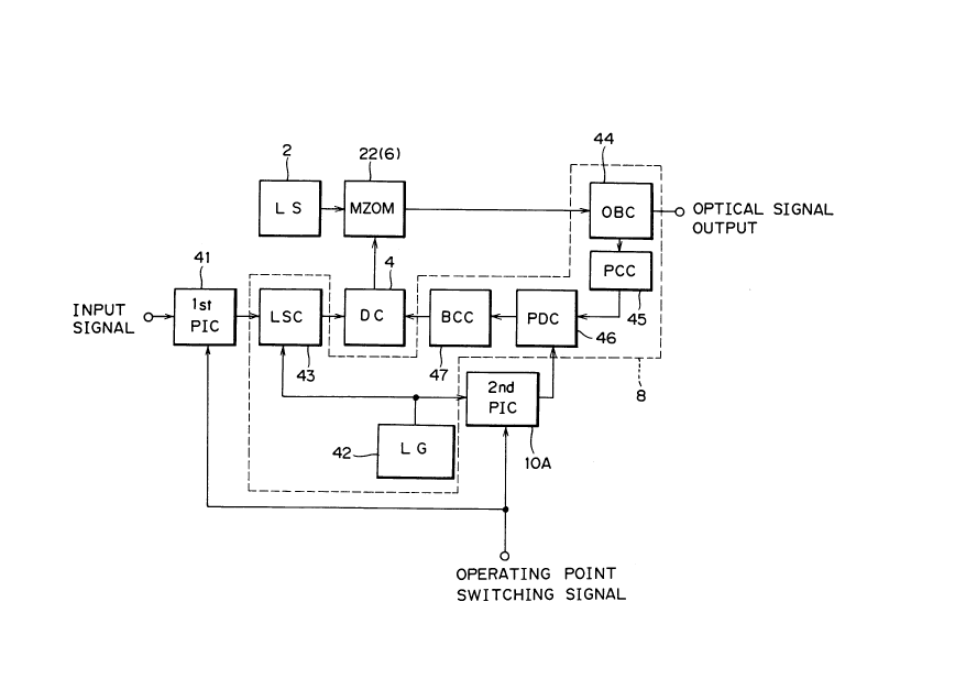
FIG.11 is a block diagram showing a first embodiment
of the optical transmitter shown in FIG.3. By the use of this
optical transmitter, the waveform deterioration due to the wave-
length dispersion can be prevented from occurring whether the
sign of the wavelength dispersion is positive or negative.
As the light source 2. a laser diode driven by a
stationary current can be used. The optical modulator 6 is the
~ach-Zehnder optical modulator as shown in FIG.10 the same as in
the preceding embodiment. The ~ach-Zehndcr optical modulator 22
if supplied with the driving voltage from the drive circuit 4 and
the bias voltage therefor is controlled by the action of the
operating point stabilizing circuit 8. exerted thereon through
the drive circuit 4. Reference numeral 41 denotes a first
polarity inverting circuit for inverting the polarity of lhe
input signal in response to shifting of the operating point by an
operating point shifting circuit.
The operating point stabilizing circuit 8 comprises a
low-frequency signal oscillator 42 outputting a low--frequcncy
signal wi~h a predetermined frequcncy ( = fO), a low frcqucncy
superposing circuit 43 for amplitude-modulating thc inpul signal
with the above described low-frequency signal and delivering the
23
20373~1
modulated signal to the drive circuit 4, an optical branching
circuit 44 for branching the optical signal output from the Mach-
Zehnder optical modulator 22, a photoelcctric converting circuit
45 for converting one of the branched optical signals inlo an
electric signal, a phase detcctor circuit 46 detecting lhe fre-
quency component of the aforesaid low-frcquency signal included
in the above described electric signal and comparing thc phase of
the frequency component with the phase of the low--frequency
signal, thereby outputting a D.C. signal with the polarity corre-
sponding to the phase difference and at the level corresponding
to the operating point drift, and a bias control circuit 47 for
feedback-controlling the bias for the Mach-Zehnder optical modu-
lator 22 so that the above D.C. signal may become zero.
The phase detector circuit 46 can be formcd of a
mixer, a low pass filter, and the like the same as in the
preceding embodiment. The bias control circuit 47 can be
constructed with an operational amplifier or the like.
As the operating point shifting circuit in the present
embodiment, a second polarity inverter circuit 10A for inverting
the polarity of the low-frequency signal input to the phasc
detector circuit 46 (shifting the phase of the low--frequency
signal by 180) in response to an operating point switching
signal is used.
FIG.12 is a diagram for explaining preferred opcrating
points on the operational characteristic curve. Referring to
24
2037351
this diagram, the operating point A represents the middle point
of the falling portion of the operational characteristic curve
and the operating point B represents the middle point of thc
rising portion of the curvc. I`IC.13 is a diagram showing various
waveforms obtained during thc operations at thc operating point
A, and FIG.14 is a diagram showing various waveforms obtaincd
during the operations at the operating point B.
In the following description, EOrepresents the
amplitude of an input optical electric-field, ~ O rcpresents the
angular frequency of the input optical electric-field, t repre-
sents time, and ~ A and ~ B represent the phases modulated with
the driving voltage waveform VD(t) in the divided waveguide paths
37A and 37B. ~ AO and ~ BO respectively represent phase changes in
the optical electric-field produced in the divided waveguide
paths 37A and 37B when VD(t) is 0. VB and VB' rcpresent bias
voltages.
Neglecting the loss produccd wilhin thc optical modu-
lator, the optical electric-field in each portion may be
expressed as follows.
Input optical electric-field:
ElN(t) = EocOs(~ O t) ...(1)
Optical electric-field at the output portion of the
divided waveguide path 37A:
EA (t) = EocOs (~ o t + ~ A (VD (t))+~ AO) /~r2 ...(2)
Optical electric-field at the output portion of the
20373Sl
divided wavcguide path 37B:
EB (t) = EocOs(~ O t + ~ B (VD (t))+~ BO) /~ 2 ...(3)
Output optical electric-field:
Eou~(t) = (EA (t)+ EB (t))/ ~r2
= E /2 . (X2 +Y2 ) I/2 . COS(~ O t-tan -'(Y/X))
... (4)
where
X = COS ( Ç!~ A (VD (t))+ ~ AO)
+ COS ( ~ B (VD (t))+ ~ B O) . . . (5)
Y = sin(~ A (VD(t))+ ~ Ao)
+ sin(~ B (V D (t))+ ~ B O) . . . (6
The variation in the wavelength is expressed, using
the phase-modulation term tan~'(Y/X) of expression (4), as
follows.
By representing the phase component ~ O t- tan-'(Y/X)
of the optical electric-field of cxpression (4) by ~ (t), the
angular frequency of the output light ~ (t) = d(~ (t))/dt.
Then, from the wavelength A (t) = 2~c/~ (t),
A (t) = 2~c/~ (t)
= 2~C/(~o ~ d(tan~'(X/Y))/dt). ...(7)
Meanwhile, the output light intensity
Pout(t) =(Eo/2)2- (X2+Y2) ...(8)
If the voltage applied to the traveling wave electrode
39 is increased, the phase of the light propagated through the
divided wavcguide path 37A leads, while the phase of the light
26
-- 2037351
propagated through lhe divided waveguidc path 37B lags. More
specifically, because of the asymmelry of the mountcd eleclrodes,
the electric field on the divided waveguide path 37A becomes
stronger than the electric field on ~he divided waveguide path
37B and, hence, thc phase modulalion in the divided wavcguidc
path 37A becomcs grcater. Thus, whcncver thc vollage applicd to
the travcling wave electrode 39 is increased, thc phasc of thc
output light of this modulator comes lo lead. Un the olher hand,
when the voltage applied to the traveling wave electrode is
increased, the light intensity may incrcase or decrease depending
on the initial phase difference between the light beams propa-
gated through the divided waveguide paths 37A and 37B. Changing
the operating point corresponds to changing the initial phase
difference between the light beams propagated through the divided
waveguide paths 37A and 37B by the control of the bias voltage.
Thus, it becomcs possible to allow the phase of the light to lead
or lag at the time of rise of the output optical pulse by chan--
ging the condition whereby the opcraling point is sel up. When
the phase leads, the wavelength is temporarily shortcned, whereas
when the phase lags, the wavelength is temporarily prolonged. In
this way, by setting up the operating point, the change in the
wavelength taking place in the output optical pulse can be sct to
be either from short wavelength to long wavelength or from long
wavelength to short wavelength.
In the present embodiment, since there is providcd lhe
-- 20~73~1
first polarity inverting circuit 41 for inverting the polarity of
the input signal according to the shifting of the operating
point, the correspondence between the polarity of the input
signal and the polarity of the output light waveform is held
unchanged as shown in FIG.13 and FIG.14, when the operating point
is shifted by half a cycle on the operational charactcristic
curve so that the wavelength within thc optical pulse may be
changcd as described above.
When the optical modulator is driven at the operating
point A, the first half of the output optical pulse comes to have
longer wavelength and thc second half thereof comes to have
shorter wavelength. When the optical modulator is driven at the
operating point B, the first half of the output optical pulse
comes to have shorter wavelength and the second half thereof
comes to have longer wavelength.
Changes in the eye pattern obtained as the results of
simulation when the optical modulator is driven at the operating
point A and the operating point B and the then obtained optical
outputs are transmitted through optical fibers whose wavelength
dispersion is ~600 ps/nm and -600 ps/nm are shown in FIG.15. The
bit rate of the input signal at that time was 10 Gb/s. Further,
I ~A I I ~R I =5:1. When the wavelength dispersion is
positive, the eye pattern is improved when the modulator is
driven at the operating point A, whereas when the wavclength
dispersion is ncgative, the eye pattern is improved when thc
28
20373~1
-
modulator is driven at the operating point B. Thus, whether the
sign of the wavelength dispersion is positive or negative, the
waveform deterioration due to the wavelength dispersion can be
prevented from occurring.
In the present embodiment, the second polarity inver-
ting circuit 10A for inverting the polarity of the low-freguency
signal input to the phase detector circuit 46 according to the
operating point switching signal is used as the operating point
shifting circuit 10. FIG.16 is a graph showing relationships
between the bias voltage for the optical modulator 22 and the
output of the phase detector circuit 46. The broken line indi-
cates the case where the polarity of the low-frequency signal is
not inverted and the solid line indicates the case where the
polarity of the low-frequency signal is inverted. By means of
feedback control performed by the bias control circuit 47, the
bias voltage, when the polarity is not inverted, is brought to
the stabilized voltage at YB1 and the bias voltage, when the
polarity is inverted, is brought to the stabilized voltage at
YB2. In this way, by inverting the polarity of the low-frequency
signal input to the phase detector circuit 46, the operating
point can be shifted so that the effect of the wavelength disper-
sion may be minimized.
FIG.17 is a block diagram showing a second embodiment
of the optical transmitter shown in FIG.3. In this embodiment,
there is provided a third polarity inverting circuit 10B as the
29
2037351
_
operating point shifting circuit, instead of the second polarity
inverting circuit 10A in the first embodiment, for inverting the
polarity of the low-frequency signal input to the low-frequency
signal superposing circuit 43 according to the operating point
switching signal. That is, the operating point of the optical
modulator 22 is shifted not by inverting the polarity of the low-
frequency signal input to the phase detector circuit 46 but by
inverting the polarity of the low-frequency signal input to the
low-frequency signal superposing circuit 43.
PIG.18 is a block diagram showing a third embodiment
of the optical transmitter shown in FIG.3. In this embodiment, a
fourth polarity inverting circuit 10C is used, as the operating
point shifting circuit 10. for inverting the polarity of th~
feedback loop in the photoelectric converting circuit 45, the
phase detector circuit 46. or the bias control circuit 47.
Also in the second and the third embodiment, the
effect of the wavelength dispersion can be minimized, the same as
in the first embodiment, by shifting the operating point of the
~ach-Zehnder optical modulator 22 by half a cycle on the opera-
tional characteristic curve according to the wave dispersion
characteristic of the optical fiber used as the optical transmis-
sion line.
FIG.19 is a graph showing the relationship between the
wavelength dispersion and the power penalty for explaining the
effects in the embodiment of the optical transmitter shown in
2037351
_,.
FIG.3. The broken line corresponds to the device of the prior
art, the solid line corresponds to the present embodiment in
which an optimum operating point is set up according to the sign
of the wavelength dispersion, and the one-dot-chain line
corresponds to the case where there is no wavelength variation in
the light source Here, the power penalty is what is dcfined as
follows
(Power Penalty) = 10 log,O(the minimum received light
power when there is wavelength dispersion / the minimum received
light power when wavelength dispersion is zero) (dB)
It is known from FIG.19 that the resistivity to the
wavelength dispersion is greatly improved over that in the prior
art by the present invention Further, it is known that the
resistivity to the wavelength dispersion is improved even over
that in the case where there is no variation in the wavelength
(where the phase-modulating efficiencies are 1:1) by the present
invention
According to the present invention, as described so
far, good transmission characteristics can bc obtained whcthcr
the wavelength dispersion of the optical fiber is positive or
negative, and allowable dispersion can be enlarged in the system
used in the zero-dispersion wavelength region of an optical fiber
and, thereby, transmission over a longer distance can be achieved
According to the present invention, the polarity of an
optical signal is inverted by shifting the operating point of an
31
2037351
_
optical modulator on the characteristic curve and, Lherefore,
such method to shift the operating point of an optical modulator
on the characteristic curve is also useful as a method for merely
inverting the polarity of an optical signal.
In the foregoing description, the present invention
has been described as related to specific embodiments, but the
invention is not limited to the details of such embodimen~s. For
example, in the embodiment (shown in PIG.11, FIG.17, and PIG.18)
of the optical transmitter of PIG.3, the transmission characteri-
stics can be improved, the same as in the case where the polarity
of the input signal is inverted, not by inverting the polarity of
the input signal by means of the first polarity inverting circuit
but only by shirting the operating point of the optical modulator
by half a cycle on the operational characterislic curve. In such
case, because the polarity Or the signal is inverted, il is
desirable that a means for matching lhe polarity Or the signal is
separately provided in the receiver or the like. The preferred
embodiments described herein are therefore illustrative and not
restrictive. Since the scope of the invention is defined in the
appended claims, modification and variation falling within the
equivalence of bounds of the claims are all within the scope of
the present invention.