Note: Descriptions are shown in the official language in which they were submitted.
-
2037~88
TITLE OF THE INVENTION
Communication terminal equipment
BACKGROUND OF THE INVENTION
1. Field of the Invention
The present invention relates to communication
terminal equipments which perform data communication with
party terminals whose data communication rates are dif-
ferent from those of the caller terminal equipments and
more particularlY, to a communication terminal equipment
of a simple structure, which allows data communication
with any party terminal having a data communication rate
different from that of the caller terminal equipment.
2. DescriPtion of the Related Art
RecentlY, integrated services digital network (ISDN)
and the corresponding various sorts of data exchange
networks connectable with the ISDN have become widelY in
use, and various types of terminals have been used in
these networks. Data communication has been increasingly
carried out between these different types of terminals.
In the data communication between these different
types of terminals, it sometimes occurs that the data
communication rate of a terminal is different from that
of another terminal. In such a case, matching of the
data communication rate among terminals must be made by
changing the data communication rate of at least one
terminal.
Referring to Fig. 3, an ISDN 200 is connected with a
`~L.
- 2037488
terminal 101 havin~ a data communication rate of 64 KbPs
and also with another data exchange network 300 which in
turn is connected with another terminal 102 having a data
communication rate of 56 Kbps. Data communication be-
tween the terminals 101 and 102 can be established by
means of interwork between the ISDN 200 and the data
exchange network 300. The data communication is required
to be carried out at the data communication rate of the
terminal 101 of the ISDN 200 which is smaller than that
of the other terminal, that is, at 56 Kbps.
For data communication between different types of
two terminals, a matchinq circuit must be provided for
matching of their data communication rates. In the case
where a PluralitY of PartY terminals have respectivelY
different data communication rates, respectively differ-
ent matching circuits must be provided depending on these
data communication rates and be selectivelY used as
necessary, thus involving a complicated circuit configu-
ration and a hlgh cost.
SUMMARY OF THE INVENTION
It is therefore an object of the present invention
to provide a communication terminal equiPment which can
realize suitable matching between a plurality of differ-
ent data communication rates with a simPle circuit con-
figuration.
In accordance with an aspect of the present inven-
tion, there is Provided a communication terminal equip-
2037~88
ment which allows data communication with a party termi-
nal having a data communication rate different from that
of the terminal equipment, and wherein mask timing is
set to Periodically delete a synchronizing clock of the
data communication rate of the communication terminal
equipment on the basis of the data communication rate of
the PartY terminal, a receive data is received from the
PartY terminal in synchronism with the sYnchronizing
clock and also the reception is made invalid at the mask
timing, and a send data is transmitted to the party
terminal in synchronism with the synchronizing clock also
with the send data being added with a predetermined dummy
bit at the mask timing.
In the present invention, when the mask timing is
set for periodically deleting the sYnchronizing clock,
the receive data received in synchronism with the syn-
chronizing clock is made invalid at the mask timing while
a dummy bit is added to the send data to be transmitted
in synchronism with the synchronizing clock at the mask
timing. For this reason, the mask timing is set to be
suitable for each of a Plurality of different data commu-
nication rates, proper matching with each data communica-
tion rate can be realized.
According to the present invention, when the mask
timing is set to be suitable for each of a plurality of
different data communication rates, proper matching with
each data communication rate can be realized. ~s a
result, there can be provided a communication terminal
equipment which can avoid a comPlicated circuit configu-
~ ~037488
ration and a high cost.
BRIEF DESCRIPTION OF THE DRAWINGS
Fig. 1 is a block diagram of a communication termi-
nal equiPment in accordance with an embodiment of the
present invention;
Fig. 2 is a timing chart showing waveforms of sig-
nals appearing at various points in the embodiment of
Fig. 1; and
Fig. 3 shows a schematic example of two terminals
having different data communication rates and communica-
tion networks connected between the two terminals.
DESCRIPTION OF THE PREFERRED EMBODIMENTS
An embodiment of the present invention will be
detailed with reference to the attached drawinss.
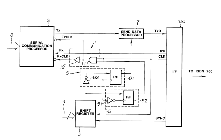
Referring to Fig. 1, there is shown a block diagram
of a communication terminal equipment in accordance with
an embodiment of the present invention.
In the drawing, a terminal interface circuit 100,
which is connected to the ISDN 200 of Fig. 3, receives a
signal at a data communication rate of 64 KbPs from the
ISDN 200 and outPuts a 64Kbps reception data RxD and a
synchronizing clock CLK together with a synchronizing
signal SYNC synchronous with the clock CLK. The terminal
interface circuit 100 also receives a transmission data
TxD from its terminal side and sends it to the ISDN 200.
The synchronizing clock CLK issued from the terminal
~ 2037488
interface circuit 100 is received at a send/receive
synchronizer 1 where a receive synchronizins clock RxCLK
and a send synchronizing clock TxCLK are generated. The
receive and send synchronizing clocks RxCLK and TxCLK are
sent from the send/receive synchronizer 1 to a serial
communication processor 2.
The processor 2 receives a data Rx from the terminal
interface circuit 100 in synchronism with the receive
synchronizing clock RxCLK, and sends to a send data
processor 7 a data Tx (to be transmitted) recelved from a
data bus 8 in synchronism with the send synchronizing
clock TxCLK.
A shift register 3 receives parallel mask timing
data from a system bus 4 in response to a reception of
the synchronizing signal SYNC from the terminal interface
circuit 100.
A first data transmitter 5 receives the synchroniz-
ing clock CLK from the terminal interface circuit 100 and
the serial mask timing data from the shift register 3,
and sends the mask timing data to the send/receive syn-
chronizer 1 serially on a bit-bY-bit basis ih synchronism
with the synchronizins clock CLK.
A second data transmitter 6 receives the synchroniz-
ing clock CLK from the terminal interface circuit 100 and
the serial mask timing data from the shift register 3,
-and sends the mask timing data to the send data processor
7 serially on a bit-bY-bit basis in synchronism with the
sYnchronizing clock CLK.
Fig. 2 shows a timing chart of waveforms of signals
2037488
at various polnts in the present communication terminal
equiPment. The exemplary oPeration of the equipment will
be detailed by referring to this timing chart. Assume
now that, as shown in Fig. 3, the present communication
terminal equipment 101 havin~ a data communication rate
of 64 Kbps is connected to the ISDN 200 while the commu-
nication party terminal 102 having a data communication
rate of 56 Kbps is connected to the data communication
network 300.
In this case, through the interwork between the ISDN
200 and the other data communication network 300, a
64Kbps data issued from the communication terminal equiP-
ment 101 is deleted by one bit for every 8 bits and
converted into a 56Kbps data which in turn is received at
the party terminal 102.
A 56Kbps data emitted from the party terminal 102,
on the other hand, is added by one invalid for every 7
bits and converted into a 64Kbps data through the inter-
work between the ISDN 200 and the other data communica-
tion network 300, and the converted 64Kbps data is re-
ceived at the communication terminal equipment 101.
First, in resPonse to a rising edge in the synchro-
nizing signal SYNC (shown by Fig. 2(b)) issued from the
terminal interface circuit 100, a mask timing data (shown
bY Fig. 2(c)) on the system bus 4 is input to the shift
register 3. The mask timing data has such a format as
shown by Fig. 2(i), that is, has a value "1" for the
first to seventh bits and has a value '0" for the last
2037~88
eighth bit as shown in Fig. 2(d).
In the first data transmitter 5, the synchronizing
clock CLK of 64KbPs from the terminal interface circuit
100 is received at a NOT circuit 51 and then sent to a
flip-flop 52 so that the fliP-flop 52 loads the mask
timing data from the shift register 3 and sends it to the
send/receive synchronizer 1 on a bit-by-bit basis in
response to a falling edge in the synchronizing clock
CLK. As a result, the mask timing data is inPut from a
flip-floP 52 of the first data transmitter 5 to an AND
circuit 11 of the send/receive transmitter 1 with a time
lag of half a period (shown by Fig. 2(f)) of the synchro-
nizing clock CLK with respect to the input timing of the
mask timing data into the shift register 3.
The AND circuit 11 of the send/receive synchronizer
1 also receives the sYnchronizing clock CLK of 64Kbps
from the terminal interface circuit 100 to find a logical
'-OR" of the received clock CLK and the mask timing data
received from the fliP-flop 52 and outputs a send sYn-
chronizing clock TxCLK (shown by Fig. 2(g)) indicative of
the found logical "OR". Since the mask timing data from
the fliP-flop 52 has a value "0" at the timing of the
eighth bit of the synchronizing clock CLK as a result of
the logical "OR", it means that the eighth bit of the
send synchronizin~ clock TxCLK is deleted. The send
sYnchronizins clock TxCLK is applied to the serial commu-
nication processor 2 and also to a NOT circuit 12.
The NOT circuit 12 inverses the send synchronizing
clock TxCLK received from the AND circuit 11 of the
2037488
send/receive synchronizer 1 to form a receive synchroniz-
ing clock RxCLK (shown bY Fig. 2(h)) and sends the re-
ceive synchronizing clock RxCLK to the serial communica-
tion processor 2.
Since the serial communication processor 2 sequen-
tlally receives the receive data RxD of 64Kbps from the
terminal interface circuit 100 in synchronism with fall-
ing edges in the receive sYnchronizins clock RxCLK, the
processor 2 substantially receives the data Rx corre-
sponding to the first to seventh bits of the receive data
RxD, with the eighth invalid bit being deleted.
Further, when the same mask timing data as in the
previous case is input from the system bus 4 into the
shift register 3 in response to the next rising edge in
the synchronizing signal SYNC, the same receiving oPera-
tion as the previous one is carried out so that the
serial communication Processor 2 receives the 64Kbps
receive data RxD from the terminal interface circuit 100
but with the eighth invalid bit being deleted. When the
receive data RxD is subjected to the deletion of one bit
for every 8 bits through such repetitive receiving opera-
tion, the effective 56Kbps data Rx from the part terminal
102 can be extracted from the 64Kbps receive data RxD
obtained by adding one invalid bit for every 7 bits and
convertins into the 64Kbps data through the interwork
between the ISDN 200 and the other data exchange network
300.
In the second data transmitter 6, then, a flip- floP
2037488
61 receivlng the 64Kbps sYnchronizing clock CLK from the
terminal interface circuit 100 sequentiallY loads the
mask timing data from the shift register 3 through a NOT
circuit 62 on a bit-by-bit basis in resPOnse to a rising
edge in the synchronizing clock CLK, and sends.an inver-
sion of the loaded mask timing data to the send data
processor 7. As a result, the inverted mask timing data
is sent from the flip-flop 61 to the send data processor
7 with a delay of the synchronizing clock CLK by one
period with resPect to the inPut timing of the mask
timing data into the shift register 3.
The serial communication Processor 2 sequentially
sends the data TX (to be transmitted) received from the
data bus 8 to the send data Processor 7 in synchronism
with falling edges in the send sYnchronizing clock TxCLK.
The data Tx is sequentially sent to the send data Proces-
sor 7 at the timing of falling edges in the first to
seventh bits of the synchronizing clock CLK while the
data Tx is not sent thereto at the timing of the falling
edge of the eighth bit thereof.
The send data Processor 7 sequentially receives the
data Tx from the serial communication processor 2, se-
quentially adds a preset dummy bit to the received data
at the rising timing of the inverted mask timing data
received from the second data transmitter 6, that is, at
the risins edge of the eishth bit of the sYnchronizins
clock CLK, and the outPUtS it to the terminal interface
circuit 100. That is, the send data processor 7 receives
the data Tx from the serial communication processor 2,
_ 2037488
adds the dummy bit to the received data Tx a~ the timing
of the eighth bit of the sYnchronizing clock CLK to form
a send data TxD, and then sends the data TxD to the
terminal interface circuit 100. In this connection, the
dummy bit is Previously set to exhibit a value of "0" or
"1". In the Present embodiment, when the dummy bit is
set to have a value "1", the send data processor 7 can
comprise an OR gate which receives the data Tx from the
serial communication Processor 2 and the inverted mask
timing data from the second data transmitter 6.
When one dummY bit is sequentially added through the
repetition of the aforementioned transmitting operation,
the send data TxD is transmitted as a 64Kbps data from
the communication terminal 101, subjected to deletion of
one dummy bit for every 8 bits thereof through the inter-
work between the ISDN 200 and the other data exchange
network 300 to be converted into a valid 56Kbps data, and
then received at the Party terminal 102.
As discussed above, in the present embodiment, on
the basis of the mask timing data having the first to
seventh bits set to have all a value "1" and the eighth
bit set to have a value "0", one bit is deleted for everY
8 bits of the 64Kbps receive data to extract the valid
56kbps data from the 64Kbps receive data, one dummy bit
is added for every 7 bits of the valid 56Kbps data to
form a 64Kbps send data to be transmitted, whereby the
caller terminal can realize data communication with the
PartY terminal having a data communication rate of
2037488
56Kbps.
Similarly, when the first to sixth bits of the mask
timing data are set to have all a value "1" and the
seventh and eighth bits thereof are set to have both a
value "O", 2 bits are deleted for everY 8 bits of the
receive data on the basis of the mask timin~ data to
extract a 48Kbps data from the 64Kbps receive data, two
dummy bits are added for everY 6 bits of the 48kbps data
to form a 64Kbps send data to be transmitted. In this
case, the caller terminal can achieve data communication
with the party terminal having a data communication rate
of 48Kbps.
Therefore, only by ProPerlY setting the mask timing
data, communlcation with the party terminals having a
Plurality of dlfferent data communication rates can be
realized and the need for switching exclusive circuits
for matching with the respective party terminals can be
eliminated.