Note: Descriptions are shown in the official language in which they were submitted.
91-03-01 19: 36 T- #759-03
2~37~91
Syste~ Bu~ Control Sy~tem ln
Multi-P,occ~r Syetem
Bao~qround of the Inventlon
Fleld of the Invention
The present inventlon generally relates to a
sy~tem bu~ control ~y~tem ln a multl-proce~-or sy~tem
and, more partlcularly, 18 directed to ~ syetem bus
utlllzatlon requeet ~y~tem, an lnter-unlt
aommunicatlon ~ystem ln a multl-proce~or ~yetem
employlng a syetem bu~ of a tlme spllt tran~for ~ystem
and a multl-proces~or ~ystem havlng a ~har-d memory
De wrl~tlQn of the Prlor Art
A mult~-proce~sor 3ystem has recsntly been used
to construct a aontrol unlt of a aomputer, an
el~ctronlo ~wltchlng ey~tem and the llko ~n thl~
~ystem, a plurallty of proceesor~ are lnterconnected
vls a slngle ~ystem b w to ~hare hardware and software
resourae~, thereby lmproving throughput, exp~n~blllty
and roliablllty
Furthermore, a bus arblter for controlllng and
~rbltratlng a utillzatlon rlght of a sy~tem bu~ le
acce~ed, to enable a plurallty of proces~or~ to
tran~mit an~ recelve data between them and other
prOae8~0re ViA the ~lngle sy~tem bu~ and a memory to
- 2 2~37~91
be interconnected to the system bus.
Figure 1 is a schematic block diagram showing an
example of an arrangement of a conventional multi-
processor system having such a bus arbiter.
S Referring to Figure 1, a plurality of CPU
~central processing unit) boards (processor units)
CPU0 to CPUN, memory boards (memory units) CMo to CMN
and a bus arbiter ~BA) 12 are interconnected to a
system bus 11. The bus arbiter 12 is adapted to
control and arbitrate the bus utilization right of
each board.
Figures 2A and 2B show arrangements of CPU board
CPUi (i = 0, 1, . . . , N) and memory board CMj,
respectively. As shown in Figure 2A, each CPU board
CPUi is composed of a microprocessor ( ~ P) 15, a
control register (CTLREG) 16 and a bus interface (BIF)
14 and, as shown in Figure 2B, each memory board CM;
is composed of a RAM (random access memory) 18, a RAM
controller 17 and the bus interface 14. The bus
interface 14 controls the interconnection between a
local bus 13 and the system bus 11 within the board.
A data transfer system called a time split system
is know for a system bus in the multi-processor
system. In this system, a command transfer cycle and
an answer transfer cycle are separated.
91-B3-01 la:37 T- #7~9-04
2037~91
Figure 3 18 a diagram ~howing an example of a
tlmlng ln which a command and an answer are
transmitted ln the oyotem bus of the tlme spllt
transfer sy~tem. ~his ex~mple llluotrate~ a c~e
where a CPU board CPUi reads dsta D ~tored in a
memory ~ddre~ A from a memory CM~.
CPVl of a CPU board tran~mlts a bu~ requeot
oignal RQl to the bu9 arblter 12 before transm~ttlng a
command C and a memory addres~ A to memory CM~. When
receiving a transfer perml~slon signal GRl from the
arblter 12, the CPU board CPUi transmlt~ the command C
and the memory addreas A to the memory board CM~
through the oy~tem bus 11. When recelv1ng the
command C and the memory addre~e A through the ~ystem
buo 11, the memory board CM~ tran~mltJ the transfer
request ~ignal RQl to the bu~ arblter 12 ln order to
transmit an anower AN and the data D etorea ln the
memory addre~s A to the CPU board CPUl. When
r~c61vlng the tran~fer permisslon signal GR~ from the
bu~ arbltor 12, the memory board CM~ transmits the
an~wor AN and the data D to the CPUl via the oystem
bu~ 1 1 .
A~ de~crlbed above, ln the system bu~ of the
conventional tlme split tranefer 8y9tem, when each CPU
2S board tran~mlts the command C or the an~wer AN, each
2~37491
CPU board must transmit the bus request signal to the
bus arbiter 12 individually.
Figure 4 is a block circuit diagram of the bus
interface 14 provided within each CPU board CPUi and
memory board CMj.
As shown in Figure 4, the bus interface 14
includes a transmission FIFO 21 of a first in first-
out system which stores transmission data and a
reception FIFO 22 of a first-in first-out system which
stores reception data. Buffers 23, 25 and buffers
24, 26 are respectively provided between these FIFOs
21, 22, the local bus 13 and the system bus 11.
Transmission data are temporarily stored in
buffer 23 and then in the transmission FIFO 21.
Transmission data sequentially read out of the FIFO 21
are tempor~rily stored in the buffer 24 and then
transmitted to the system bus 11.
Reception data are stored in buffer 26 and then
stored in the reception FIFO 22. Reception data
sequentially read out of the reception FIFO 22 are
temporarily stored in buffer 25 and transmltted to the
local bus 13.
Reception control units 27, 30 and transmission
control units 28, 29 are adapted to control the
writing and reading of these buffers 23 to 26 when
_ 5 _ 2 03 7 ~9 l
data are transmitted and received. Transmission FIFO
control unit 31 and a reception FIFO control unit 32
are adapted to instruct a write address and a read
address of the transmission FIFO 21 and the reception
FIFO 22, respectively.
Figure 5 is a block diagram showing a specific
arrangement of the transmission FIFO control unit 31
which is shown by the hatched portion in Figure 4.
As shown in Figure 5, an input address unit 33 is
a circuit which instructs the write address of the
transmission FIFO 21 and outputs and address, which is
sequentially incremented by [1], to the transmission
FIFO 21 in accordance with a signal supplied thereto
through an OR gate 34 from the reception control unit
27 or from the transmission control unit 29. of the
write addresses output from the input address unit 33,
a breakpoint address of transmission data row is
stored in a queue buffer 35. An output of the OR
gate 34 is supplied to the transmission FIFO 21 as a
data write signal WE and data are written into the
transmission FIFO 21 in response to the data write
signal WE.
The output address unit 36 is a circuit which
instructs a read address of the transmission FIFO 21
and outputs addresses, which are sequentially
- 6 - 2037~91
incremented by [1], to the transmission FIFO 21 in
accordance with the read signal from the transmission
control unit 28. The read address of the output
address unit 36 and the breakpoint address of the
transmission data row of the queue buffer 35 are
compared by a comparator 37, and the reading of data
in the transmission FIFO 21 is continued until the two
addresses coincide.
An input completion display FF 38 is a flip-flop
which is set by a signal from the reception control
unit 27 or from the transmission control unit 29 via
the OR gate 39 upon data transfer, and an output
completion display FF 40 is a flip-flop which is set
when the data transfer is finished.
A comparator 41 compares the outputs of flip-
flops 38 and 40 to determine whether a command C or an
answer AN transfer request signal RQ should be
transmitted from the transmission control unit 28 or
not.
For example, when the input completion display FF
38 is set and the output completion display FF 40 are
reset, data to be transferred remain so the comparator
41 detects that the outputs of FFs 38 and 40 are not
coincident. Thus, the transmission control unit 28
outputs the command C or the answer AN transfer
91-03-01 lB: 38 T- t~759-05
2037491
r~qUeBt 8 ignal RQ .
In this tlme ~pllt transfer sy3tem, durlng the
ldle period other than that ~ n whlch the command C or
the an~wer AN i~ output, the system bus 11 i~ opened
5 to each board. However, it l~ frequently observed
th~t tho ~ystom bus 11 is occupled between partlcular
~oard~ to perform data transfer, whlch 18 called a
lock transfer.
Flgure 6 l~ a diagram showlng exarnples of the
10 command C format and the an~wer AN u~ed in the lock
tran~fer. A~ shown ln Flgure 6, the command C ls
composed of data f~ eld lndlcating destinatlon, data
fleld lndicatlng the unit from whlch data 15
transmltted, data field indlcatlng the lclnd of data
and dat~ field lndicat~ng the data transfer amount.
Al~o~ the an~wer AN 18 composod of data ~leld
indlcatlnq destlnation, data fleld lndlcatlng the unlt
from whlch dsta i8 trAnsmitted, data ~1eld lndlcatlng
the klnd of data and data fl-ld of an~wer code.
Flgure 7 i~ a diagram use~ to explaln the
operation of the sy~t~m upon lock tran~fer. The bus
arblter ~BA) 12 iB arranged such th~lt, wh~n recelvlnq
th~ lock tran~fer ~lgnAl~ the bUB arblter 12
recognlz~ the destlnatlon board from the deotlnatlon
25 data in the command C to recelve only the transfer
91-03-01 13: 39 T- #759-06
2~37~91
-- 8 --
request from the destinatlon board 80 a3 to tran3fer
the answer AN.
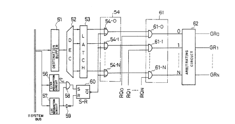
Fl~ure 8 i~ a clrcult block dlagram showing a
main portion of the bu~ arbiter. Referenc~ will be
made to this flgure ln explainlng the bus arblter'~
functlon of recelvlng only the transfer reque~t from
the de~tlnstlon board upon a loc~ tr~n~fer.
Referring to Flgure 8, destinatlon data ln the
command C i8 ~tored ln a destination buffer 51 and the
destlnatlon data i8 decoded by a decoder ~DEC) 52.
The decoded data iB thereby output to an OR gate group
54.
The command and the lock tr~n~fer signal are
re~pectlvely input to a C/AN recognitlon clrcult 56
and a lock recognition clrcuit 57. Outputg from
the~e recognlt~on circuit~ 56 and 57 are supplled
through an AND gate 58 or an lnverter 53 to a s~t
ter~inal S or a re~et terminal R of an RS flip-flop
~RS-~F) 60. A ~ output of the RS-~F 60 1~ ~upplled
to one input terminal of OR gate~ 54-1 (1 - O, 1,
N) of the OR gate group 54. When the lock transfer
~ignal is lnput to the RS-FF 60 and the Q output of
the RS-FF 60 goes low level, one input termlnal of OR
gates 54-1 of the OR gate group 54 all become low level
a~d only the other lnput termlnal of OR gate 54-i
91-03-01 18:40 T- #759-07
9 ~0374~1
corre~ponding to the de6tlnatlon data stored ln the
de~tlnatlon buffer 51 become6 hlgh level. Thus, of
AND gate group 61, only AND gate 61-1 coxrespondlng to
the destlnatlon data 18 opened to permlt the transfer
reguest ~lgnal from the destlnatlon data to be lnput
to an arbltratlng clrcult 62.
~ he arbltratlng clrcult 62 issue~ a tran~fer
perml~slon 31gnal GRl correspondlng to the transfer
reque~t elgnal output from the AND gate group 61 at
its AND gate 61-i corresponding to the destinatlon
data. Upon lock tr~n~fer, only the tranefer requ88t
~lgnal from the de~ignated destlnation data stored ln
the destinatlon buffer 51 becomes actlve and 1~ lnput
to the arbltratlng circuit 62 8~ descrlbed abov~, with
the re~ult that the tran~fer perml~slon slgnal G~l (1
~ 0, 1, ..., N) can be transmitted only to the
de~ignated destination board.
In the data tran~fer sy~tem of the tlme split
~ystem, the bus arbiter control~ the transfer requ2~t
~lgnal~ of c~. s~ds ~nd an~wer3 from the re~p~ctlve
boards lnterconnected to the ~y~tem bu~ and
s0quentlally lssues the tran~fer permlBBion slgnal ln
the order of bDard~ having highest prlority.
When the CPU board CPUl transfers the command and
aw~lts the an~wer from the memory board CM~, lf the
- 10 - 2~37~91
command transfer request signal is output from a CPU
board CPUn having higher priority, then the transfer
permission signal is issued to the CPU board CPUn and
the transfer of answer from the memory board CMj to
the CPU board CPUi is awaited.
In general, the local bus 13 within the CPU board
CPUi is of the interlock type such that the local bus
13 is held until it receives the answer from the
destination board. Consequently, when the time split
transfer system is utilized as the data transfer
system of the system bus, there arises a problem that,
until the answer is being returned, other units within
the board cannot utilize the local bus 13. Further,
when the lock transfer system is employed as the data
transfer system of the system bus, the system bus can
be occupied only by a particular board so that the
answer waiting time can be reduced. However, the
circuit must be constructed such that the bus arbiter
12 identifies the destination board so that it
receives only the transfer request from it and
refuses transfer requests from other boards. Thus, a
complicated circuit arrangement cannot be avoided.
The time split transfer system is effective for
decreasing a system bus occupying ratio and for
increasing a system bus utilization ratio in a
11 ~03~91
particular CPU board (hereinafter referred to as a
processor unit) in the multi-processor system.
In a multi-processor system employing a system
bus which is not based on the time split transfer
system, the occupying ratio in which the system bus is
occupied by a particular processor unit is increased
because such a processor unit exclusively occupies the
system bus when it is allowed to use it. In the time
split transfer system, however, such restriction does
not occur because a plurality of processor units
utilize the system bus in a time sharing manner,
allowing other processor units to sequentially utilize
the system bus without awaiting the answer to the
access request. Therefore, respective processor
units can execute different processings via the single
system bus.
In either of the above two bus systems, an
apparatus (hereinafter referred to as a unit) is
requested to be connected to the system bus so as to
input and output data in a data width different from
the bus width inherent in the system bus in accordance
with the expansion of system function.
An example of an arrangement of such system is
represented in the schematic block diagram in Figure
9 Figure 9 shows the arrangement of the multi-
2V~7491
processor system which employs the time split transfer
system system bus.
In this system, a system bus 100 includes a bus
width information line 106 in addition to a data bus
102 and an address bus 104, and a plurality of units
110-1, 110-2, ..., 110-N are connected to the system
bus 100.
A data transfer operation of this system will be
described below with reference to a timing chart of
Figure 10.
Referring to Figure 9, when other unit 100-j (j =
1, 2, ..., N; i = j) is accessed via the bus width
information line 106 by a certain unit 110-i (i = 1,
2, ..., N) of a plurality of units 110-1, 110-2, ....
110-N, data and addresses are transferred through the
data bus 102 and the address bus 104. Bus width
information is also transferred through the bus width
information line 106. When the reception unit 100-j
receives the bus width information, the reception unit
100-j can identify the bus width of transferred data
and can correctly transmit and receive data.
Incidentally, the bus width information line 106 is
occupied similarly to the data bus 102 and the address
bus 104 (see (A), (B) and (C) of Figure 10).
However, if the system shown in Figure 9 is
- 13 - 20 3 7 ~9 1
constructed by using the system bus of the time split
transfer system, as shown in Figure 11, the plurality
of units 110-1, 110-2, ..., 110-N are connected to a
system bus 103 which is formed of an address bus and a
data bus.
A data transfer operation between the units in
the system shown in Figure 11 employing the time split
transfer system, system bus will be described next with
a timing chart forming Figure 12.
However, in the time split system, the single
system bus is utilized in a time sharing fashion as
described above. According to this time split
system, before an answer (see answer AN in Figure 12)
is returned to a certain unit for a command and an
address ~see a command C1 and an address A in Figure
12) transmitted from a certain unit, a command and an
address ~see a command C2 and an address B in Fiqure
12) from another unit are transmitted so that the bus
width information cannot be held until the answer is
returned, unlike in the conventional bus system. As
a result, the transmission and reception of data
having a data width different from the bus width of
the system bus 103 (see Figure 11) cannot be
performed. There is then the problem that, in the
conventional time split system, the unit having a data
: .
~ 14- 20~7491
width different from the bus width of the system bus
cannot be utilized in the system.
A sharing memory multi-processor system is used
for sharing a hardware resource in the multi-processor
5 system. In this system, a plurality of processors
share one memory in use. To cope with control forms
which presumably become more and more complicated, a
wide variety of control must be realized by an input
and output unit which is made common to respective
10 processors interconnected to a system bus.
Figure 13 is a block diagram showing an example
of a system arrangement of a conventional sharing
memory multi-processor system.
In Figure 1 3, a shared memory (CM) 201,
respective processor units (PU1 to PU3) 210-1 to 210-3
and an input and output unit ( IOU) 220 are
interconnected to a system bus 230. The shared
memory 201 and the processor units 210-1 to 210-3 have
bus interface circuits (BIF) ZOla and 211a to 213a to
20 which individual identifiers (IDs) are assigned so
that they can recognize their own access by
determining whether the identifier (ID) transmitted on
the system bus 230 is equal to the identifiers (IDsJ
assigned to their bus interface circuits or not.
At image of a memory area which can be accessed
- 15 ~ 2~7 491
by respective processor units 210-1 to 210-3 is
represented in Figure 14. In this example, half
the memory space is utilized by a shared memory area
MC and the remaining half is utilized by local memory
area M Q of respective processor units 210-1 to Z10-3.
To access such memory space, a boundary address
for indicating a boundary of addresses and identifiers
(IDs) for the shared memory 201 are set between the
bus interface circuits (BIF) 201a and 211a to 213a so
that, when addresses of internal buses 21lb to 213b
provided within respective processor units 210-1 to
210-3 access the shared memory area Mc, as shown in
Figure 15, the shared memory 201 can be accessed via
the system bus 230 by utilizing the identifier of the
shared memory 201 set in a shared memory identifier
register 216 provided within an external bus interface
unit 216 within the bus interface circuits 211a to
21 3a of respective processor units 210-1 to 210-3.
Thus, the local memory area M Q can be independently
utilized only within respective processor units 210-1
to 210-3. In other words, respective processor
units 210-1 to 210-3 cannot access the local memory
area MQ of another processor unit. More
specifically, when a comparator 218 detects that an
internal bus address B is smaller than an address A
91-03-~ 42 T- ~759-0EI
,, .
2~37491
previously set ~n a boundary register 217 (A > a ), the
axternal bu~ lnterface unit 216 ~hown ln Flgure 15 19
enabled, and lf A < B, then the external bus interface
unlt 216 determines that the acces~ l~ the access to
5 the local memory area M ~ ~o that the external bus
lnterface unit 216 18 not enabled.
A bus lnterface clrcuit 220a of the lnput and
output unlt ~IOU) 230 shared by re~pectlve proce~or
unlt~ 210-1 to 210-3 interconnected to the system bus
230 l~ al~o arranged a~ shown ln ~igure 15. In thls
circult, the acce~s to the har~d memory are~ Mc can
be ef~ected, but the local memory area M~ of each of
the processor unlt~ 210-1 to 210-3 cannot be acces~ed.
Accordlngly, ln the conventlonal shared memory multl-
15 processor ystom, although the dlrect memory access
~DMA) tran~fer of the shared mernory area Mc can be
c~rrled out, the local memory area ~ Q of e~ch of the
processor units 210-1 to 210-3 cannot be acces~ed so
that the lnput and output unit 230 cannot perform the
20 DMA transfer to the local memory area M ~ of each of
the proce~or unlts 210-1 to 210-3 by the lnput and
output apparatu~ 220b. Thi~ cau~es the problem that
comE~lex control cannot be achieved.
SUmmArY of tho Invent~on
Th~ present lnventlon l~ made ln vlew of the
91-03-01 18: 43 T- #759-09
2037~91
"
above-mentioned backgrou~d~n~ A first ob~ect of the
present lnvention i~ to reallze, ln a bu~ arbiter
control of a multi-processor, a bue utillz~tion right
request ~ystem with a simplif~ed circuit arrangement
which can reduce awalt~ng tlme for an answer.
A ~econd ob~ect of the present inventlon i9 to
provlde an lnter-unlt communicatlon system in whlch a
plurallty of unlts having different data wldths for
proceeslng data can be fabricsted lnto a ~yatem in a
multl-processor system utllizlng a system bus of a
tlme split transfer ~y~tem.
A ~hird ob~ect of the pre~ent invention i8 to
realize a multi-proce~or sy~tom havlng a ~hared
memory in whlch an input a nd output uni t
interconnected to a eyetem bu~ can acce~ not only the
shared memory but also a local memory of an arbitrary
processor unit, thereby effectlnq a wlde varlety of
control,
To achleve the fir~t ob~ect, the present
inventlon assume6 a multl-proce~sor aystem ln which a
plurality o~ CPU boarde and memory board arc
lnterconnected to a common ~yetem bu~.
This multl-proceB5or 6y~tem is comprlsed of a bus
interface for connecting the local bu~ wlthln each of
the board~ and the ~ystem bus, a bu3 arbiter for
- 18 - 2037~91
arbitrating a system bus utilization right of each of
the boards, command transfer request lines for
transmitting a command transfer request from the CPU
boards to the bus arbiter, answer transfer request
signal lines for transmitting an answer transfer
request, and answer transfer request lines for
transmitting an answer request from the memory boards
to the bus arbiter. When the transfer request is the
command transfer request, the bus interface enables
the command transfer request signal lines, and when
the transfer request is the answer transfer reauest,
the bus interface enables the answer transfer request
signal lines. The bus arbiter identifies the command
transfer request and the answer transfer request on
the basis of the signal levels of the command transfer
request signal lines and the answer transfer request
signal lines and permits the answer transfer request
to utilize the system bus with higher priority to the
command transfer request.
In a preferred embodiment of the present
invention, the bus interface includes memory means for
storing a queue additional information indicating
whether the transfer request is the command transfer
request or the answer transfer request of a data row
at every breakpoint of the data row to be transmitted,
2037491
wherein the bus interface enables the
corresponding command transfer request lines or the
corresponding answer transfer request lines on the
basis of the queue additional information stored in
the memory means.
Further, in the preferred embodiment of the
present invention, the bus interface is composed of
judging means for judging whether or not the transfer
request signal is to be output, a first AND gate to
which are input a judged result of the judging means
and the queue additional information stored in the
memory means, and a second AND gate to which are
input the judged result of the judging means and
inverted information of the queue additional
information stored in the memory means, wherein the
bus interface circuit enables the corresponding common
transfer request signal lines via the first AND gate
and enables the answer transfer request signal lines
via the second AND gate.
A preferred embodiment of the bus arbiter is
comprised of a first arbitrating circuit, a second
arbitrating circuit and a transfer permission signal
output circuit. The first arbitrating circuit is
supplied with command transfer requests from
respective boards and enables an output terminal
- 20 - 2~37491
corresponding to a board which outputs the enabled
command transfer request having the highest priority.
The second arbitrating circuit is supplied with
answer transfer requests from respective boards and
enables an output terminal corresponding to a board
which outputs the enabled answer transfer request
having the highest priority. The transfer permission
signal output circuit is supplied with an output of
the first arbitrating circuit and an output of the
second arbitrating circuit. It gives higher priority
to the transfer permission request to the answer
transfer request output from the second arbitrating
circuit regardless of the output of the transfer
permission request to the command transfer request
from the first arbitrating circuit when the second
arbitrating circuit outputs the transfer permission
request relative to the answer transfer request. It
then outputs the transfer permission signal relative
to the answer transfer request.
In this arrangement, the bus interface enables
the corresponding signal lines by judging whether the
transfer request is the command transfer request or
the answer transfer request. When receiving the
transfer request signal, the bus arbiter identifies on
the basis of a judged result of the command transfer
- 21 - 2037491
signals lines or the answer transfer request signal
lines whether the transfer request is the command
transfer request or the answer transfer request.
Then, the bus arbiter permits the answer transfer
request to utilize the system bus with higher
priority.
Accordingly, the return of the answer is
processed with priority to the command transfer
request. Thus, the answer waiting time of the CPU
board can be reduced and the processing efficiency of
the CPU board can be enhanced.
In another preferred embodiment corresponding to
the present invention, the bus arbiter processes the
answer transfer request with priority upon lock
transfer. Then, when receiving the answer transfer
request upon lock transfer, the bus arbiter may
interrupt the lock transfer and permit the board,
transmitting the answer transfer request to utilize
the system bus.
According~y, even in the lo~k transfer, the
answer transfer request is processed with priority so
that, if only the command transfer request is locked
and an exclusive control is performed, functions
required for the lock transfer can be satisfied.
The present invention for achieving the second
- 22 - 2037491
object is based on a multi-processor system in which a
plurality of units are connected to a time split
transfer system system bus having a predetermined bus
width. Each unit includes a bus interface comprising
a receiving unit for receiving data of its own unit
from other unit and a transmitting unit for
transmitting data to other unit through the system
bus.
In the first invention relating to the second
object, the transmitting unit of the bus interface is
arranged such that an answer including bus width
information indicating a bus width of data transmitted
and received through the system bus by its own unit as
an answer to the command received via the system bus
is transmitted to the unit which transmitted the
received command.
In the second invention relating to the second
object, the transmitting unit of the bus interface is
arranged such that bus width information indicative of
bus width of data transmitted and received by its own
unit through the system bus is included in the command
transmitted to another unit via the system bus.
In a preferred embodiment of the second
invention, the receiving unit of the bus interface
includes bus width information extracting means for
- 23 - 2037~91
extracting bus width information from a received
command. The receiving unit may be arranged so as to
receive data transmitted next to the reception command
transmitted by the unit which transmits the reception
command on the basis of the bus width information
extracted by the bus width information extracting
means.
In another preferred embodiment of the second
invention, the receiving unit of the bus interface
includes bus width information extracting means for
extracting bus width information from a received
command. Furthermore, the transmitting unit of the
bus interface may be arranged such that, when the
command received by the receiving unit is a data read
command, the bus width information extracted by the
bus width information extracting means is included in
an answer relative to the received data read command,
and is returned to the unit from which the data read
command is transmitted.
In accordance with this arrangement, when
returning an answer relative to a command received
from a transmission side unit through the system bus
of the time split system, the reception side unit
inserts the bus width information output from the bus
width information output unit into the answer in a bus
- 24 - 20~7~91
width information insertion unit and returns it to the
transmission side unit.
Then the reception side unit recognizes the data
width of data received next to the reception command
by extracting the bus width information from the
reception command with the bus width information
extracting means and processes the reception data.
Accordingly, the reception side unit can
recognize the data width of the data received via the
system bus of the time split transfer system and the
transmission unit can recognize the data width of data
received via the system bus of the time split transfer
system from the reception side unit. Thus, the unit
for processing data of an arbitrary data width within
a data width of the system bus of the time split
transfer system can be interconnected to the system
bus of the time split system.
Finally, the present invention for achieving the
third object assumes a multi-processor system in which
an input and output unit, a plurality of processor
units and a shared memory commonly utilized by the
plurality of processor units are interconnected to the
system bus. Furthermore, the input and output unit
and the plurality of processor units include
individual identifiers and shared memories for reading
- 25 ~ ~0374~1
in the identifier transmitted on the system bus to
thereby determine their own access.
The bus interface for connecting the input and
output unit to the system bus determined on the basis
of the address value transmitted on the internal bus
whether the access is to the shared memory or to the
local memory within one of the plurality of processor
units. When the bus interface determines that the
access is to the shared memory, it accesses the shared
memory at its address corresponding to the address
value. When the bus interface determines that the
access is to the arbitrary processor unit, it accesses
the arbitrary processor unit at its local memory
corresponding to the address value.
In a preferred embodiment of the present
inventio~, the bus interface of the input and output
unit includes first memory means for storing the upper
or lower limit of the address of the shared memory,
and
comparing means for comparing the address stored
in the first memory means with an address transmitted
on the internal bus, wherein it is deter~ined on the
basis of a compared result of the comparing means
whether the access is to the shared memory or to the
local memory within the arbitrary processor unit.
- 26 - 2Q37491
At that time, the first memory means stores the
upper limit of the address of the shared memory and
the bus interface determines that the access is to the
shared memory when the comparing means outputs a
compared result indicating that the address
transmitted on the internal bus is smaller than the
address stored in the first memory means and
determines that the access is to the local memory
within the arbitrary processor unit when the comparing
means outputs a compared result indicating that the
address transmitted on the internal bus is larger than
the address stored in the first memory means.
In another preferred embodiment of the present
invention, the bus interface of the input and output
unit is comprised of second memory means in which the
identifier of the shared memory is stored, third
memory means in which the identifiers of the plurality
of processor units are stored, and selecting means for
selecting the identifier stored in said second memory
means and the identifier of an arbitrary processor
unit of the plurality of processor units stored in the
third memory means,
wherein when a unit body section of the input and
output unit accesses the shared memory, the shared
memory identifier stored in the second memory means is
- 27 - 2~37491
output to the system bus by the selecting means, and
when the unit body section of the input and output
unit accesses the arbitrary processor unit, the
identifier stored in the third memory means and
corresponding to the arbitrary processor unit is
output to the system bus by the selecting means,
thereby accessing the shared memory or the local
memory of the plurality of processor units.
In this arrangement, the input and output unit
can access not only the shared memory but also the
local memory of the arbitrary processor unit in the
plurality of processor units interconnected to the
system bus via the bus interface.
Brief Description of _he Drawinqs
A better understanding of the objects, features
and advantages of the invention can be gained from
the following detailed description of the preferred
embodiments, in conjunction with the accompanying
drawings, wherein:
Figure 1 is a schematic block diagram showing an
arrangement of a general multi-processor system;
Figure 2A is a schematic block diagram showing an
arrangement of a general CPU board;
Figure 2B is a schematic block diagram showing an
arrangement of a general memory board;
2037~9~
- 28 -
Figure 3 is a diagram showing an example of a
timing at which a command and an answer are
transmitted in a system bus of a time split system;
Figure 4 is a schematic block diagram showing an
arrangement of a bus interface according to the prior
art;
Figure 5 is a circuit block diagram showing in
more detail the transmission FIFO control unit shown
in Figure 4;
Figure 6 is a diagram of formats of command and
answer used in lock transfer;
Figure 7 is a schematic block diagram used to
explain the lock transfer operation;
Figure 8 is a circuit block diagram showing a
main portion of a conventional bus arbiter;
Figure 9 is a block diagram showing an
arrangement of a multi-processor system which utilizes
a system bus other than the system bus of the time
split transfer system;
Figures 10A to 10C are schematic diagrams used to
explain the data transfer operation of the system bus
in the multi-processor system shown in Figure 9;
Figure 11 is a schematic block diagram showing an
arrangement of a multi-processor system utilizing a
system bus of the time split transfer system;
2~7~91
- 29 -
Figure 12 is a schematic diagram used to explain
data transfer operation in the multi-processor system
shown in Figure 11;
Figure 13 is a schematic block diagram showing an
example of a conventional multi-processor system
having a shared memory;
Figure 14 is a schematic block diagram showing an
arrangement of memory spaces which can be accessed by
respective processor units;
Figure 15 is a circuit block diagram of
respective processor units and bus interfaces within
an input and output unit according to the prior art;
Figure 16 is a block diagram showing a multi-
processor system according to a first embodiment of
the present invention;
Figure 17 is a circuit block diagram of a bus
interface of each board in the first embodiment of the
present invention;
Figure 18 is a circuit block diagram showing a
2G bus arbiter in the first embodiment of the present
invention;
Figure 19 is a schematic block diagram showing an
arrangement o~ the multi-processor ~ystem according to
the second embodiment of the present invention;
Figure 20 is a block diagram showing a circuit
_ 30 _ ~ ~ 3 7 ~g 1
configuration of the bus interface in the second
embodiment of the present invention;
Figures 21A to 21D are diagram showing,
respectively, formats of command, answer, reception
control buffer and transmission control buffer;
Figure 22 is a block diagram showing in more
detail a portion relating to the main portion of the
present invention within the bus interface circuit
used in the second embodiment;
Figure 23 is a block diagram showing a detailed
Gircuit configuration of an answer generating unit in
the second embodiment of the present invention;
Figures 24A to 24C are timing charts to which
references will be made in explaining operation of the
second embodiment of the present invention;
Figures 25A to 25H are timing charts to which
references will be made in explaining operation timing
of the answer generating unit in the second embodiment
of the present i.nvention;
Figure 26 is a block diagram showing an
arrangement of a multi-processor system having a
shared memory according to a third embodiment. of the
present invention;
Figure 27 is a block diagram showing a circuit
arrangement of an internal bus interface unit in the
91-03-01 13:44 T- #759-10
2~37491
third e~bo~iment of the prQsent lnvention;
Figure 28 1~ a block diagram showing a circult
arrangement of an external buQ interface unit ln the
third embodiment of the pre~ent inventlon; and
Flgure 29 i~ a timing chart to whlch reference~
will be made ln explaining the operatlon of the thlrd
embodlment.
Detailed Descrlptlon of the Preferred Embodlments
The preferred embodiment~ of the present
lnventlon will hereinafter be descrlbed with roference
to the accompanylng drawlngs.
Flgure 16 1 8 a block diagram showing an
arrangem~nt of a multi-processor sy~tem accordlng to a
flr~t embodlment of the pre~ent inventlon.
lS A~ shown ln Figure 16, CPU board~ CPUO to CPUN
and a bus arbiter 301 are lnterconnected by command
tran~Per reque~t slgnal lines Lco and LCM through
which c~. r ~"fl transfer request slgnAls RQci (1 ~ O,
1, . ~ . , M) are transmltted ~nd answer transfer
request oign~l llnes ~pO to LpM through which answer
tran6fer reque~t signal~ RQpl tl . 1, 2, . . ., M) are
tran~mitted. Al~o~ memory board3 CMo to CMN and the
bu~ arbiter 301 are interconnected by an~wer transfer
request slgnal llnes ~MO to LMN through whlch the
answer tran~er reque6t slgnal~ RQM1 from the memory
- 32 - ~ ~37~91
boards CMj (j = 1, 0, . . . , N) are transmitted, and
the bus arbiter 301 and the respective boards are
interconnected by signal lines GRpi (i = 0, 1, . . . .
M) and GRMj (j = 0, 1, . . . , N) through which a
transfer permission signal GR is transmitted.
In this embodiment, a high [H] level signal is
assigned to the answer transfer request signals RQpi
and RQMj and also a high [H] level signal is assigned
to the command transfer request signal RQci, whereby
the bus arbiter 301 recognizes the answer transfer
request or the command transfer request by detecting
whether the transfer request signal is at high or low
level.
Figure 17 is a block diagram of a circuit
arrangement of a bus interface within a CPU board CPUi
and a memory board CMj.
Figure 17 shows the circuit mainly relating to
the transmission. The same circuit block as in of the
conventional bus interface (Figures 4 and 5) are
marked with the same reference numerals and need not
be described.
As shown in Figure 17, a queue additional
information buffer 312 is provided to store
information indicating the status of the transfer
request signal, or whether the transfer request signal
gl-03-01 18: 47 T- #759-12
2~3~
iB the command transfer requQst or the answer transfer
request.
An output of the queue additional buffsr 312 1B
lnput directly to an AND gate 313 and also in the
5 inverted ~ignal form. These AND gates 313 and 314
are supplled at the other input termlnale with a
comparsd output of comparator 41 whlch detects the
pre~ence or absence of data which ls not yet
tran~ferred. If data to be tran~ferred stl~l
remains, a s~gnal corresponding to the queue
additional lnformatlon i8 output to the tran~mlsslon
control unit 28. When the queue additlonal
lnformatlon 16, for example, the an6wer transfer
request, both lnputs of the AND gate 314 are enabled
~nd an output thereof becomes high level. In
re~ponee to the high level output of ~he AND gate 314,
th~ tran~misslon control unlt 28 txansmlt~ the answsr
tranefer request slgnal RQH to the ~n~wer trAn~fer
request ~lgnal llnes Lpl and LpJ.
When the queue additlonal lnformatlon 18 the
command tran~fer request, both lnputs of the AND gate
313 are enabled and the output thereof goe~ to hi~h
level, whereby the transmls~lon control unlt 28
transmits a command transfer request sl~nal RQL of
hlgh level to the command transfer reque~t ~lgnal llne
~ 34 ~ 2~37491
Lci.
Thus, the bus arbiter 301 can recognize the
answer transfer request or the command transfer
request by determining whether the transfer request
signal is at high level or low level.
Further, since the queue additional information
buffer 312 stores the queue additional information
indicative of any one of the command transfer requests
or answer transfer requests at every breakpoint of the
data row stored in the transmission FIFO 21, the
content of the transfer request can be analyzed within
a short interval.
Figure 18 is a block diagram showing an example
of an arrangement of the bus arbiter 301.
As shown in Figure 18, command transfer requests
RQLo to RQLN (RQCo to RQCM) of low priority level and
answer transfer requests RQHpo to RQHpN, RQHMo to
RQHMN (RQpo to RQpM, RQMo to RQMN) from the respective
boards are input to the bus arbiter 301.
Arbitrating circuits 325 and 326 are provided to
determine the priority in processing the command
transfer request RQL1 and the answer transfer requests
RQHpi and RQHMj from the respective boards. The
arbitrating circuits 325 and 326 store the priority
orders assigned to the respective boards, and when a
_ 35 2037491
plurality of boards simultaneously output the answer
transfer requests and the command transfer request,
the arbitrating circuits 325 and 326 output the high-
level signal from the output terminals corresponding
to the high priority boards.
Respective outputs of the command arbitrating
circuit 325 are input to an AND gate group 330 and
respective outputs of the answer arbitrating circuit
326 are input to a multi-input NOR gate 341 and an OR
gate group 350.
Let it now be assumed that a plurality of command
transfer requests and a plurality of answer transfer
requests are simultaneously inputted to the bus
arbiter 301. Then, the command arbitrating circuit
325 and the answer arbitrating circuit 326 output
high-level signals from their output terminals
corresponding to the highest-priority boards in the
respective command and answer requests. At that
time, due to the output of the answer arbitrating
circuit 326, one input of the NOR gate 341 goes to
high level so that the output of the NOR gate 341 goes
to low level, causing one input terminals of all AND
gates 330-i of the AND gate group 330 to go to low
level.
Consequently, the command transfer request input
- 36 - -2 Q~
to the AND gate group 330 is ignored and the transfer
permission signals GRi, GRj are output to the
highest-priority board in which outputs the answer
transfer requests.
Further, at that time, if there is another answer
transfer request, the output of the NOR gate 341
similarly goes to low level so that the transfer
permission signal is output with priority to the
answer transfer request.
Since the command transfer request signal line
RQci, the answer transfer request signal lines Lci and
Lcj, and the arbitrating circuits 325 and 326
corresponding individually to these request signal
lines are provided as described above, the command
transfer request and the answer transfer request are
discriminated and transmitted to the bus arbiter 301
from the respective boards. Thus, the two request
signals can be discriminated from each other at the
bus arbiter 301 side.
Further, since the two signals can be
discriminated, the answer transfer request can be
processed with higher priority. In addition, these
functions can be realized with a bus interface and bus
arbiter with simpler circuit arrangements than the
conventional bus interface and bus arbiter.
2037491
- 37 -
Therefore, since the answer is immediately
returned to the CPU board CPUi which issues the
command, it becomes possible to reduce the time during
which the CPU board CPUi is set in the answer awaiting
condition. As a result, a local bus placed in the
inter-lock system can be more effectively utilized to
enhance the processing efficiency of each board.
Further, when a lock transfer is carried out in
the prior art, a transfer request from another board
is neglected. Therefore, the bus arbiter must include
a circuit for recognizing a board to which the lock
transfer is addressed and a circuit for receiving only
the answer request from that board. These circuits
are not needed in the present invention. More
specifically, the answer transfer request is processed
with a priority such that, if the lock transfer is
carried out only on the command transfer request and
an exclusive control is performed, then the answer
transfer request can be processed while the bus
utilization right between the CPU board which outputs
the lock transfer command and the destination board is
maintained.
The CPU boards and the memory boards described in
this embodiment are not limited to microprocessors or
boards having memories. The present invention can
91-03-01 1~: 45 T- ~759-11
.
~7~
al~o be applled to an exclusive control in a large
~cale sy~tem ln whlch a ~y~tem formed of a plurality
of boards is con~idered as one processlng apparatus
and a plurallty of the above-mentloned proceRsing
apparatuse~ are interconnected to a network or an
upper cla~s bu~.
A~ descrlbed above, ~ccording to the present
invsntlon, the an~wer transfer re~ueBt i8 procegeed
wlth hlgher prlorlty to the command tran~fer reque~t
,by ~ 61mply arrsnged bus lnterface and ~us arblter.
~hus, even when the system bus 1~ utilized by the
data tran~fer ~y~tem of the time ~plit transfer
~ystem, the time durlng which the CPU board which
output~ the command i6 Bet in the an~wer waiting
aondltion can be reduced and the proce~lng efficlency
~f the system can be increa~ed.
A second embodlment of the pre~ent lnventlon i8
d~scrlbed next.
Flgure 19 i9 a schematic block diagram ~howlng
one portlon of an ~rrangement of a multi-proce~or
~y~tem according to the ~econd embodiment of the
2û
pre~nt lnvention.
AB Jhown ln Flgure 19, a unit 500 and a unit 600
are connected to a ~y~tem bus 401 formed of an addre~s
bus and a data bus via bu~ interfaces (BIFs) 510 and
610 whlch are reepectlvely provlded w~thin the units.
~5
2~374.~
The unit 500 transmits and receives data of 64-bit-
wide data to and from another unit through the system
bus 401, and the unit 600 transmits and receives 32-
bit-wide data to and from another unit through the
5 system bus 401.
The bus interfaces 510 and 610 within the units
500 and 600 have the same circuit arrangement, and
Figure 20 shows a block circuit diagram of the bus
interfaces 510 (610~.
10As shown in Figure 20, the bus interface 510
(610) is composed of a receiver 511, a driver 51 2,
reception register 514, a system bus recepti.on control
unit 515, a reception buffer (BF) 516, a reception
control buffer (RSB) 518, an internal bus interface
15circuit 520, a transmission register 522, a
transmission buffer (SB) 524, a system bus
transmission control unit 525, a transmission control
buffer (SSB) 526, a driver 528 and a receiver 530.
The receiver 511 and the driver 512 are connected to
2~ the system bus 401 of the time split system, and the
driver 528 and the receiver 530 are connected to a
local bus 555.
The reception register 514 is a register which
temporarily stores a command, data or the like
25 transmitted from other units and received from the
-- 40 --
2~37~91
system bus 401 through the receiver 511, and the
received data is output to the reception buffer 516.
The system bus reception control unit 51 5
contains a counter. Each time reception data is
stored in the reception register 514, the unit 515
increments the counter by [1] and supplies the count
value to the reception buffer 516 as a reception
buffer write address. Also, the system bus reception
control unit 515 generates a reception control buffer
write address into which reception control data
(described later) is written and supplies this data
to the reception control buffer 518.
The reception control buffer 51 8 stores
informations necessary to control received data. This
information includes a pointer indicating the
starting position of received data, the kind of
command, data length (bytes) of received data and so
on, which will be stored in the reception buffer 516
as will be described moxe fully later. The reception
control information is utilized when the local bus
interface circuit 520 transmits data stored in the
reception buffer 51 6 through the driver 528 to the
local bus 555.
The local bus interface circuit 520 then and
writes local data input through the receiver 530 to
- 41 - 2~37491
the local bus 55 in the transmission buffer 524. It
also generates an answer to be transmitted to another
unit via the system bus 401.
The transmission buffer 524 temporarily stores
5 data to be transmitted to another unit, and this data
is written by the local bus interface circuit 520.
The transmission control buffer 526 has a function
fundamentally similar to that of the reception control
buffer 518 and stores therein information necessary to
10 control the transmission data stored in the
transmission buffer 524, as described more fully
later.
The system bus transmission control unit 525
transmits data stored in the transmission buffer 524
15 through the transmission register 522 and the driver
51 2 to the system bus 401 on the basis of the
transmission control information stored in the
transmission control buffer 526.
Formats of the command C and the answer AN
20 transmitted by each unit through the system 401 to
another unit and formats of control information
written in the reception control buffer 518 and the
transmission control buffer 526 are represented in
Figures 21A~ 21B 21C and 21D, respectively.
The command C is formed of a destination unit
_ 42 - 2~3~9~
number DU, a sending unit number SU, bus width
information BW, read/write information RW and so on as
shown in Figure 21A. The answer AN is composed of a
destination unit number DU, a sending unit number SU,
bus width information BW and so on as shown in Figure
21B.
As described above, the command C and the answer
AN both include the bus width information BW. Thus,
when transmitting the command C, the transmitting side
unit can let the receiving side know the bit width of
the data transmitted by its own unit. Also, when
transmitting the answer AN, the unit which receives
the command C can let the unit which transmits the
command C know the bit width of data transmitted by
its own unit through the system bus 401.
The reception control information that the
reception control buffer 518 generates at every piece
of data written in the reception buffer 516 is
composed, as shown in Figure 21C, of a pointer P
indicating the starting position of reception data in
the reception buffer 516, read/write information R/W
indicating the kind of reception data, a bus width
information BW indicating bit width of reception data,
a byte number indicating data length of reception
data, a sending unit number SU indicating the number
_ 43 _ 2037491
(ID) of the unit which transmits the reception data
and so on.
The transmission control information that the
transmission control buffer 526 generates at every
5 piece of data written in the transmission buffer 524
is composed of, for example, a pointer P indicating a
starting position of transmission data within the
transmission buffer 524, bus width information BW
indicating bit width of transmission data, a byte
10 number bit BT indicating data length of transmission
data, etc.
Figure 22 shows more fully a main portion of the
bus interface circuit 510 (610) which relates to the
present invention.
As shs~wn in Figure 22, an internal bus interface
circuit 520 is composed of an internal bus access
control unit ~IBC) 520a and an answer generation unit
520b.
The internal bus access control unit 520a
20 supplies a reception control buffer read address to
the reception control buffer 518 to read out from the
reception control buffer 518 the reception control
information of the format shown in Figure 21B. Then,
the internal bus access control unit 520a reads out
25 individually D1, D2, . . . from the reception buffer
_ 44 _ 2037491
516 with reference to the pointer P within the
reception control information. The internal bus
access control unit 520a transmits the thus read-out
reception data D1, D2, . . . formed by the command C,
etc. having the format shown in Figure 21A to the
local bus 555. Also, the internal bus access control
unit 520a is supplied with response data to the
command C through the local bus 555 and outputs the
response data and the byte number BT of the response
data to the answer generation unit 520b together with
the answer generation instruction.
When receiving the answer generation instruction
from the internal bus access control unit 520a, the
answer generation unit 520b reads out the bus width
information BW corresponding to the command C
transmitted to the local bus 555 and the sending unit
number SU from the reception control buffer 518.
Subsequently, the answer generation unit 520b
generates the answer AN of the format shown in Figure
21B and writes it and data input via the local bus 555
in the transmission buffer 524. It also writes the
pointer P indicating the write address of the answer
AN into the transmission buffer 524, and the byte
number information BT and other information into the
transmission control buffer 526. The writing of data
2037~1
in the transmission buffer 524 and the transmission
control buf fer 526 is performed such that data are
written in the addresses instructed by transmission
buf fer write address and transmission control buf fer
5 write address supplied from the answer generation unit
520b to the transmission buffer 524 and the
transmission control buffer 526.
The transmission buffer 524 and the transmission
control buffer 526 both include two ports. These
10 ports are supplied with the transmission buf fer read
address and the transmission control buffer read
address, respectively, from the system bus
transmission control unit 525. In other words, the
two buffers 524 and 526 are provided with two ports so
15 that the write and read can be performed
simultaneously .
Figure 23 is a block circuit diagram showing the
answer generation unit 206 more in detail.
As shown in Figure 23, the answer generation unit
20 520b is composed of a sending unit number register
(SUR) 604, a selector (SEL) 606, a sending buffer
write address generation unit 608 and a timing control
unit 610.
The timing control unit 610 receives the answer
25 generation instruction from the internal bus access
- 46- 2037491
control unit 5ZOa.
The selector 606 alternatively selects, in
response to a selection signal from the timing control
unit 610, data from the internal bus access control
5 unit 620a, the sending unit number SU stored in the
sending unit number register 604, the bus width
information BW from the reception control buffer 526
and other information from the answer generation unit
520b. Input data are sequentially written into the
10 transmission buffer 524 at its storage position
designated by a starting transmission buffer write
address (address determined hy the transmission
pointer) applied from the transmission buffer write
address generation unit 608 to the transmission buffer
15 524. In this writing operation, a transmission
buffer write signal (SB write signal) is supplied to
the transmission buffer 524 from the timing control
unit 610. The transmission pointer is transferred to
the transmission control buffer 526 together with the
20 byte number information BT from the internal bus
access control unit 520a and other information ~ETC)
and written in the storage position designated by the
transmission control buffer write address supplied
from the answer generation unit 520b to the
25 transmission control buffer 526. In this writing
- 47 - 2037491
operation, a transmission control buffer write signal
(SSB write signal) is supplied from the timing control
unit 610 to the transmission control buffer 526.
Operation of the thus arranged second embodiment
is described with reference to timing charts in
Figures 24A to 24C and Figures 25A to 25H.
Initially, a read operation from a unit
(hereinafter referred to as a reception unit) accessed
by another unit via the system bus 401 of the time
split transfer system is described. This description
assumes that the bus width of the unit (transmission
unit) which issues a data read command is 32 bits.
The reception unit receives reception data
through the receiver 511 and the reception register
514 of the bus interface 510 (6l0) shown in Figure 20.
Reception is executed by analyzing the 32-bit-wide
command (see the read command C2 of Figure 5; A is the
address and this address is 32 bits wide) set in the
reception register 514. More specifically, when the
read/write information WR determines that the
destination unit number DU of the reception command
set in the read R is coincident with the unit number
of its own unit, the reception is started. Then,
reception control information of one unit
corresponding to the data written in the reception
- 48 - 2037491
buffer 516, that is, the reception control information
composed of the pointer P, the read information R, the
bus width information BW, the byte number BT, the
sending unit number SU and other information ETC is
written in the reception control buffer 518. Of the
reception control information 518, the read
information R, the bus width information BW, the
sending unit number SU and other information ETC are
set in the reception command.
Also, the pointer P indicates the pointer value
in the read command reception time controlled by the
system bus reception control unit 515, and the byte
number BT is a value which results from counting the
number of bytes of data transferred after the command
by the system bus reception control unit 515. The
internal bus interface circuit 520 reads out the
reception data from the reception buffer 516 at its
storage position designated by the pointer P read out
from the reception control buffer 518 by the reception
control buffer read address transmitted from the
internal bus access control unit 520a at a
predetermined timing with the reception of this data,
for example, in a parallel condition.
The internal bus interface circuit 520 reads out
from the reception control buffer 38 the read/write
~ 49~ ~037~91
information WR, the bus width information BW, the byte
number BT, the sending unit number SU and other
information ETC to thereby access the local bus 555.
This aecess is carried out in accordance with the
5 conventional system.
A transmission operation for translnitting data
transferred from the local bus 555 in response to the
read command by the reception unit will be described
next .
When the result of access ( read ) to the local bus
555 is transferred to the internal bus access control
unit 520a, the internal bus access control unit 520a
transmits an "H" (active) level answer generation
instructing signal ( see Figure 25B) to the answer
15 generation unit 520b. When receiving the answer
generation instructing signal, the timing control unit
610 outputs an "L" (low) level selection signal (see
Figure 25E), and by this selection signal, the answer
information is initially supplied through the selector
606 to the transmission buffer 524 (see AN of Figure
25H). In parallel thereto, the timing control unit
610 generates a transmission buffer write address
generation signal, and in response to this
transmission buffer write address generation signal, a
transmission buf fer write address generation unit 608
~ 50- '2~37491
generates a transmission pointer P. The
aforementioned answer information is written into the
transmission buffer 524 at its storage position
designated by the transmission pointer P output from
5 the transmission bus write address generation unit
608, i.e., at the starting position of the
transmission information when the SB write signal (see
Figure 25D) is supplied from the timing control unit
610 to the transmission buffer 524. In the sending
10 unit number storaqe area within the storage position
contains the answer information (see Figure 25B),
there is written the sending unit number SU from the
reception control buffer 518 as the destination unit
number DU; in the sendinq unit number storage area,
15 there is written its own unit number SU read out from
the sending unit number register 604; in the bus width
information storage area, there is written the bus
width information BW read out from the reception
control buffer 518; and in the other information
20 storage area, there is written other information ETC
generated from the internal bus access control unit
520a. Subsequently, the transmission pointer P, the
bus width information BW read out from the reception
control buffer 518 and other information ETC are
25 written into the transmission control buffer 526 at
- 51 _ 2037491
its storage position designated by the transmission
control buffer address (see Figure 25F) generated by
the answer generation unit 520b when the SSB write
signal (see Figure 25C) is supplied thereto from the
5 timing control unit 610.
After this, answer information AN is written into
the transmission buffer 524, by the "H" level
selection signal output from the timing control unit
610. The selector 606 then selects the access result
10 data from the internal bus access control unit 620a
and outputs the selected data to the transmission
buffer 524. This access result data is a data width
determined by the bus width information BW, that is,
the width of 32 bits~ That data is sequentially
15 written into the transmission buffer 524 at its
storage position next to the storage position
designated by the above-described transmission pointer
(see D1 and D2 of Figure 25H). The address (see
Figure 25G) used in this writing is formed by the
20 transmission pointer. At the completion of the
writing, the byte number BT and other information ETC
determined in response to the data amount written in
the transmission buffer 524 by this writing are
transferred from the internal bus interface circuit
25 520 and written in the byte number storage area and
- 52 _ 203~4~1
other information storage area within the transmission
control information storage area of the transmission
control buffer 526.
At a predetermined timing with this writing in
5 the transmission control buffer 526, the reading from
the transmission control buffex 526 is performed, for
example, in a parallel fashion, by the read address
determined by the read control by the system bus
transmission control unit 525. This read address
10 then becomes the aforementioned transmission control
buffer read address and thereby starts the data read
from the transmission control buffer 526. With this
data read, transmission control information of format
shown in Figure 21D is read out from the transmission
control buffer 526. The data read is then started
from the transmission buffer 524 at its storage
position designated by the transmission pointer P
within the transmission control information.
Transmission information initially read out by this
20 data read is the answer information. This answer
information is transmitted to the system bus 401
through the transmission register 522 from the driver
512. Furthermore, it is transmitted through the
system bus 401 to the unit which transmits the read
25 commans~, that is, the unit which transmits the access
_ 53 _ 2037491
request. In transmitting this answer information,
the bus width information BW of the transmission
information read out from the transmission control
buffer 526 is employed, and the answer AN of the
5 format shown in Figure 21B is transmitted via the 32-
bit-wide system bus 401 (see AN2 of Figure 24; this
AN2 is the answer to the command C2).
After the answer AN2 is transmitted, the data
read is continued from the storage position next to
10 the storage position indicated by the transmission
pointer P of the transmission buffer 524 to the
storage position determined by the byte number BT
within the transmission control information. The
data width of this read-out data is 32 bits wide.
1~, The access request unit then receives the bus
width information BW within the answer AN transferred
via the system bus 401 and also receives data
transferred next by the 32-bit width indicated by the
bus width information BW. That is, the unit which
20 issues the data-read command can read data from
another unit in a suitable data width.
A writing operation in the reception unit
accessed by another unit via the system bus 401 of the
time split transfer system is described. It is
25 assumed that the reception unit bus is 64-bit wide and
2~374~
- 54 -
the system bus 401 is 64-bit wide. This operation is
the same as the read out operation for the reception
unit except for the following points.
Firstly, read/write information within the 32-bit
wide command received is the write information W and
the 32-bit-wide address A is simultaneously
transferred via the system bus 401. Secondly, 64-
bit-wide data is transmitted after the command and the
address. Thirdly, the number of bytes written into
the reception control buffer 518 is the number of
bytes constituting the data received. Fourthly, the
byte number written into the transmission control
buffer 526 is "0" because no data is to be
transmitted. Accordingly, only the 32-bit-wide
answer AN1 is written into the transmission buffer
524. Incidentally, remaining 32-bit data written in
the transmission buffer 524 together with the answer
AN1 is meaningless (corresponding to the hatched
portion in Figure 24).
The command C1, address A, data D and answer AN1
illustrate an example of such a writing operation in
the reception unit having only the above differences.
The command C1, address A and the data D are
informations transferred to the reception unit and the
answer AN1 is the information returned to the unit
2037~91
which transmits the data-write command.
While the bus width information BW transferred
from the sending unit to the destination unit is
inserted into the answer to the access of the sending
unit and returned to the sending unit as described
above, a variant is also possible such that
previously-prepared bus width information BW is
inserted into the answer and returned to the sending
unit which transmits the command.
As described above, according to this embodiment,
since the bus width information BW is provided in both
the command and the answer, the receiving circuit from
the system bus of the time split transfer system can
be commonly utilized in the command reception and in
the answer reception. Thus, the circuit arrangement
of the receiving circuit is simplified.
Further, since the bus width information is
formed within the answer, while it is determined
whether or not the received answer is transmitted to
its own unit, the preparation processing for the data
reception becomes possible on the basis of the bus
width information. Conversely, if there i5 no bus
width information, the operation for the corresponding
bus width must be performed after it is determined
that the answer is transmitted to its own unit.
- 56 - 2~37~91
Therefore, according to this embodiment, the answer
processing can be executed at high speed.
As will be clear from the above explanation,
according to the second embodiment of the present
invention, since the bus width information is
inserted into the answer and this answer is returned
to the sending unit (which transmits the arbitrary
command) from the reception unit through the system
bus of the time split system, the unit which processes
arbitrary data within the data width of the system bus
of the time split transfer system can be connected to
the system bus of the time split system.
Accordingly, the present invention can be suitably
applied to the expansion of a multi-processor system
which flexibly employs the system bus of the time
split transfer system. The present invention is
excellent in expanding the multi-processor system
utilizing the system bus of the time split system.
Finally, a third embodiment corresponding to the
2~ third object is described. Figure 26 is a block
diagram showing a system arrangement of a multi-
processor system having a shared memory according to
the third embodiment of the present invention. In
Figure 26, like parts corresponding to those of Figure
13 are marked with the same references and therefore
2~7491
-- 57 --
need not be described.
In Figure 26, reference numeral 1100 designates
an input and output unit ~IOU) which is composed of an
IO unit body 1000a, an internal bus interface unit
51 000b and an external bus interface unit 1 000c.
Figure 27 shows in more detail a block circuit
diagram of the internal bus interface unit 1000b, and
Figure 28 shows in more detail a block circuit diagram
of the external bus interface unit 1000c.
10In Figure 26, reference numeral 1100 designates a
bus arbiter which performs an arbitration, such as a
decision of utilization right of the system bus 230
among the processor units 210-1 to 210-3 and the input
and output unit 1000 on the basis of the priority
order. In this embodiment, if access is made from the
IO unit body 1000a by the IO access signal IOAC, the
internal bus interface unit 1000b outputs a low level
"L" access signal IOA and a selector 2001 (shown in
Figure 28) provided in the external bus interface unit
201000c selects and outputs the contents of a processor
unit identifier register 2002 which holds the
id~ontifiers (IDs) of the respective processor units
210-1 to 210 3 so that, when the access is made by the
IO unit body 1000a, not only the shared memory 201 but
25 also the local memory M* within other processor units
_ 5~ _ 20~74~1
210-1 to 210-3 can be accessed.
The arrangement and operation is described next
with reference to the block diagrams in Figures 26 to
28 and the chart in Figure 29.
AS illustrated, when the request signal REQ
output from the IO unit body 1000a goes low "L" level,
address/data (data is not shown) on the internal bus
and the IO access signal IOAC are sampled via a gate
3001 and a flip-flop 3002 of the internal bus
interface unit 1000b shown in Figure 27, and an
address ADRi and the access signal IOA are output from
the internal bus interface unit 1000b and then fed to
the external bus interface unit 1000c. In that case,
if the shared memory area Mc is accessed, the access
signal IOAC goes to high "H" level and the access
signal IOA goes to low "L" level.
A register value A in the boundary register 3003
is previously determined and the register value A and
the value B of the address ADRi from the flip-flop
3002 are compared by a comparator (CMP) 3004. If the
shared memory area Mc is accessed, the value B of the
address ADRi is smaller than the register value A of
the boundary register 3003 (A > B) so that the output
of the comparator 3004 goes to high "H" level and an
output of an OR gate 3005 goes to high "H" level.
~ 59 ~ ~ ~3~
Thus, the request signal RQ to the external bus
interface unit 1000c goes to high "H" level. If the
request signal RQ goes to high "H" level, then a bus
request signal BRQ goes to low "L" level via the gate
circuit 2003 of the external bus interface unit 1000c
and applied to a bus arbiter 1100. Then, when a bus
request permission signal BACK is returned from the
bus arbiter 1100, a bus start signal BS goes to low
"L" level in the external bus interface unit 1000c.
In that casel since the access signal IOA is at low
"L" level, the selector 2001 selects the shared memory
identifier register 2004, whereby the identifier ( ID)
for accessing the content of the register 2004, that
is, the shared memory 201 is selected and output
through a gate 2005 which is set in the pass state by
the bus start signal BS. Then, the address ADRi
output from the internal bus interface unit 1000b is
also output as ADRo via a gate 2006 which is set in
the pass state by the bus start signal BS.
If the local memory area M ~ is accessed, the IO
access signal IOAC goes to low "I," level and the
access signal IOA goes to high "H" level. In that
case, since the local memory area M Q is accessed, the
value B of the address ADRi becomes larger than the
register value A of the boundary register 3003 (B >
- 60- ~03~4~
A) . Accordingly, although the output of the
comparator 3004 goes to low "L" level, the access
signal IOA is at high "H" level so that the output of
the OR gate 3005 goes to high "H" level. Thus, the
5 request signal RQ is made high "H" level. If the
request signal RQ goes to hi gh "H" level, the bus
request signal BRQ goes to low "L" level, and if the
bus request permission signal BACK is returned from
the bus arbiter 1100, then the bus start signal BS
10 goes to low "L" level. In that case, since the
access signal IOA is at high "H" level, the selector
2001 selects the processor unit identifier register
2002. Thus, the identifier for accessing the content
of the register 2002, that is, the respective
processor units 210-1 to 210-3, is selected and output
via the gate 2005, which is set in the pass state by
the bus start signal BS whose identifier (ID) is set
in the pass state. Then, the address ADRi output
from the internal bus interface unit 1000b is output
20 via the gate 2005 which is set in the pass state by
the bus start signal ~S.
In other words, in the case of the access by the
input and output unit, not only the shared memory area
Mc but also the respective local memory areas MQ of
arbitrary processor units 210-1 to 210-3 can be
~ ,, ' '
2~
- 61 -
accessed, thereby making it possible to perform a
wider variety of control than in the example of the
prior art.
The processor units 210-1 to 210-3 selected by
the identifier (ID) make a ready signal (RDY) low "L"
level which transmits the answer of normal reception,
whereby the input and output unit 100 finishes the
external bus cycle relative to the system bus 230.
Further, the ready signal RDY is converted to RDY1 by
a gate circuit 2007 in the external bus interface unit
1000c and sent to the internal bus interface unit
1000b, wherein it is converted to a ready signal READY
for the IO unit body 1000a by a gate circuit 3006.
Thus, the internal bus cycle of the input and output
unit 1000 relative to the internal bus is finished.
As described above r according to the present
invention, the bus interface of the input and output
is provided with a processor unit identifier register
(second register) and a selector for selecting the
content of the second register by the IO access signal
(IOA) so that, when the access is made by the IO unit
body, not only the shared memory area but also the
local memory area within the processor unit can be
accessed, thus making it possible to perform a wider
variety of control operation than in the example of
- 62 - ~03~9~
the prior art.
While the address space of the shared memory is
allocated to an address space of lower order than the
local memory of each processor unit in the above
embodiment, the present invention is not limited
thereto and can be easily applied to a multi-processor
system in which the address space of the shared memory
is allocated to an address space of higher order than
the local memory of each processor unit. In that
case, the output level of the compared result of, for
example, the comparator 3004 may be inverted.
Having described preferred embodiments of the
invention with reference to the accompanying drawings,
it is to be understood that the invention is not
limited to those precise embodiment and that various
changes and modifications thereof could be effected by
one skilled in the art without departing from the
spirit or scope of the invention as defined in the
appended claims.