Note: Claims are shown in the official language in which they were submitted.
-9-
The embodiments of the invention in which an exclusive
property or privilege is claimed are defined as follows:
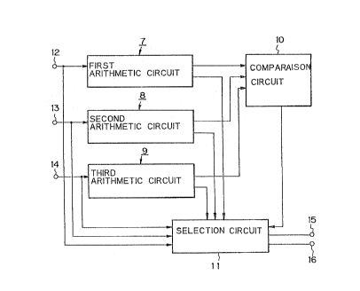
1. A diversity circuit having a plurality of input
terminals and receiving at the respective input terminals
respective received signals which have been propagated
through different signal paths, said diversity circuit
comprising:
transmission channel characteristic estimation
circuits provided to correspond to said plurality of input
terminals, each of said transmission channel characteristic
estimation circuits estimating the characteristics of the
transmission channel of each signal path on the basis of
each of said received signals to output the estimated value
of the transmission channel characteristics;
error computing circuits provided to correspond to
said respective transmission channel characteristic
estimation circuits, each of said error computing circuits
computing the power of the estimated transmission channel
characteristics on the basis of said estimated value which is
output from the corresponding transmission channel
characteristic estimation circuit, and estimating a received
signal on the basis of said corresponding estimated value
and a transmission pattern which is known in advance, to
compute a power ratio of the power of said estimated
transmission channel characteristics to the corresponding
error power between the power of the estimated received
signal and the power of said received signal;
a comparison circuit for comparing the respective
power ratios respectively output from said error computing
circuits, to output a selection signal designating the
signal path corresponding to a maximum power ratio; and
a selection circuit for outputting the received
signal and the estimated value of the transmission channel,
which correspond to said signal path designated by said
selection signal, out of said respective received signals and
said respective estimated values of the transmission channel
characteristics.
2. A diversity circuit for receiving a plurality of
received signals which have been propagated through a
-10-
plurality of different signal paths and for selecting an
optimum received signal, said diversity circuit comprising:
transmission channel characteristic estimation means
for computing an estimated value of the transmission
channel characteristics representing the estimated
characteristics of the transmission channel of the signal path on
the basis of the received signal, for each of said plurality
of received signals;
means for computing the power of the estimated
transmission channel characteristics on the basis of said
estimated value for each received signal;
means for estimating a received signal on the basis
of said estimated value and a transmission pattern which
is known in advance, for each received signal;
means for computing an error power between the power
of the estimated received signal and the power of said
corresponding received signal for each received signal;
means for computing a power ratio of said power of
the estimated transmission channel characteristics to said
corresponding error power for each received signal; and
means for comparing respective power ratios and for
selecting and outputting the received signal corresponding
to a maximum power ratio.
3. A diversity circuit as defined in Claim 2, wherein
said means for selecting and outputting the received signal
corresponding to the maximum power ratio further selects and
outputs the estimated value of the transmission channel
corresponding to the maximum power ratio.
4. A diversity circuit as defined in Claim 2, wherein
said transmission channel characteristics comprise a channel
impulse response.
5. A diversity circuit as defined in Claim 2, wherein
said transmission channel characteristic estimation means,
said means for computing the power of the estimated
transmission channel characteristics, said means for estimating a
received signal, said means for computing the error power,
and said means for computing the power ratio are provided to
respective received signals.
-11-
6. A frame phase (or sampling tuning) estimation circuit
using a diversity circuit, comprising:
a delay circuit for providing a received signal with
a plurality of different delays to output a plurality of
differently delayed received signals,
said diversity circuit including:
transmission channel characteristic estimation
circuits provided to correspond to said plurality of differently
delayed received signals, each of said transmission
channel characteristic estimation circuits estimating the
transmission channel characteristics on the basis of each of
said plurality of differently delayed received signals to
output the estimated value of the transmission channel
characteristics;
error computing circuits provided to correspond to
said respective channel characteristic estimation circuits,
each of said error computing circuits computing the power of
the estimated transmission channel characteristics on the
basis of said estimated value which is output from the
corresponding transmission channel characteristic estimation
circuit, and estimating a received signal on the basis of
said corresponding estimated value and a transmission
pattern which is known in advance, to compute a power
ratio of the power of said estimated transmission channel
characteristics to the corresponding error power between the
power of the estimated received signal and the power of said
received signal;
a comparison circuit for comparing the respective
power ratios respectively output from said error computing
circuits, to output a selection signal designating the
delay corresponding to a maximum power ratio; and
a selection circuit for outputting the delayed
received signal and the estimated value of the transmission
channel, which correspond to said delay designated by said
selection signal, out of said plurality of differently
delayed received signals and said respective estimated
values of the transmission channels.
-12-
7. A frame phase (or sampling timing) estimation circuit
using a diversity circuit, comprising:
a delay circuit for providing a received signal with
a plurality of different delays to output a plurality of
differently delayed received signals,
said diversity circuit including:
transmission channel characteristic estimation means
for computing an estimated value of the transmission
channel characteristics on the basis of each of said
plurality of differently delayed received signals;
means for computing the power of the estimated
transmission channel characteristics on the basis of said
estimated value for each differently delayed received
signal;
means for estimating a received signal on the basis
of said estimated value and a transmission pattern which
is known in advance, for each differently delayed received
signal;
means for computing an error power between the power
of the estimated received signal and the power of said
corresponding delayed received signal for each differently
delayed received signal;
means for computing a power ratio of said power of
the estimated transmission channel characteristics to said
corresponding error power for each differently delayed
received signal; and
means for comparing respective power ratios and for
selecting and outputting the delayed received signal
corresponding to a maximum power ratio.
8. A frame phase (or sampling timing) estimation circuit
as defined in Claim 7, wherein said means for selecting and
outputting the received signal corresponding to the maximum
power ratio further selects and outputs the estimated value
of the transmission channel corresponding to the maximum
power ratio.
9. A frame phase (or sampling timing) estimation circuit
as defined in Claim 7, wherein said transmission channel
characteristics comprise a channel impulse response.
-13-
10. A frame phrase (or sampling timing) estimation
circuit as defined in Claim 7, wherein said transmission
channel characteristic estimation means, said means for
computing the power of the estimated transmission channel
characteristics, said means for estimating a received
signal, said means for computing the error power, and
said means for computing the power ratio are provided to
respective received signals.
11. A diversity circuit having a plurality of input
terminals and receiving at the respective input terminals
respective received signals which have been propagated
through different signal paths, said diversity circuit
comprising:
a transmission channel characteristic estimation
circuit provided for each of said input terminals, each
of said transmission channel characteristic estimation
circuits estimating the characteristics of the
transmission channel of the signal path corresponding to
the input terminal on the basis of the corresponding
received signal to output the estimated value of the
transmission channel characteristics;
an error computing circuit provided for each of
said respective transmission channel characteristic
estimation circuits, each of said error computing
circuits computing the power of the estimated
transmission channel characteristics on the basis of said
estimated value which is output from the corresponding
transmission channel characteristic estimation circuit,
and estimating a received signal on the basis of said
corresponding estimated value and a predetermined
transmission pattern, to compute a power ratio of the
power of said estimated transmission channel
characteristics to a corresponding error power of the
difference between the estimated received signal and said
received signal;
a comparison circuit for comparing the power
-14-
ratios output from said error computing circuits, to
output a selection signal designating the signal path
corresponding to a maximum power ratio; and
a selection circuit for outputting the received
signal and the estimated value of the transmission
channel, which correspond to said signal path designated
by said selection signal.
12. A diversity circuit for receiving a plurality of
received signals which have been propagated through a
plurality of different signal paths and for selecting an
optimum received signal, said diversity circuit
comprising:
transmission channel characteristic estimations
means for computing an estimated value of the
transmission channel characteristics representing the
estimated characteristics of the transmission channel of
the signal path on the basis of the received signal, for
each of said plurality of received signals;
means for computing the power of the estimated
transmission channel characteristics on the basis of said
estimated value for each received signal;
means for estimating a received signal on the
basis of said estimated value and a predetermined
transmission pattern, for each received signal;
means for computing an error power of the
difference between the estimated received signal and said
corresponding received signal for each received signal;
means for computing a power ratio of said power of
the estimated transmission channel characteristics to
said corresponding error power for each received signal;
and
means for comparing respective power ratios and
for selecting and outputting the received signal
corresponding to a maximum power ratio.
13. A diversity circuit as defined in Claim 12,
-15-
wherein said means for selecting and outputting the
received signal corresponding to the maximum power ratio
further selects and outputs the estimated value of the
transmission channel corresponding to the maximum power
ratio.
14. A diversity circuit as defined in Claim 12,
wherein said transmission channel characteristics
comprise a channel impulse response.
15. A diversity circuit as defined in Claim 12,
wherein said transmission channel characteristic
estimation means, said means for computing the power of
the estimated transmission channel characteristics, said
means for estimating a received signal, said means for
computing the error power, and said means for computing
the power ratio operate on said received signals in
parallel.
16. A frame phase (or sampling timing) estimation
circuit using a diversity circuit, comprising:
a delay circuit for providing a received signal
with a plurality of different delays to output a
plurality of differently delayed received signals,
said diversity circuit including:
a transmission channel characteristic estimation
circuit provided for each of said differently delayed
received signals, each of said transmission channel
characteristic estimation circuits estimating the
transmission channel characteristics on the basis of said
plurality of differently delayed received signals to
output the estimated value of the transmission channel
characteristics;
an error computing circuit provided for each of
said respective transmission channel characteristic
estimation circuits, each of said error computing
circuits computing the power of the estimated
-16-
transmission channel characteristics on the basis of said
estimated value which is output from the corresponding
transmission channel characteristic estimation circuit,
and estimating a received signal on the basis of said
corresponding estimated value and a predetermined
transmission pattern, to compute a power ratio of the
power of said estimated transmission channel
characteristics to a corresponding error power of the
difference between the estimated received signal and said
received signal;
a comparison circuit for comparing the power
ratios output from said error computing circuits, to
output a selection signal designating the delay
corresponding to a maximum power ratio; and
a selection circuit for outputting the delayed
received signal and the estimated value of the
transmission channel, which correspond to said delay
designated by said selection signal.
17. A frame phase (or sampling timing) estimation
circuit using a diversity circuit, comprising:
a delay circuit for providing a received signal
with a plurality of different delays to output a
plurality of differently delayed received signals,
said diversity circuit including:
transmission channel characteristic estimation
means for computing an estimated value of the
transmission channel characteristics on the basis of each
of said plurality of differently delayed received
signals;
means for computing the power of the estimated
transmission channel characteristics on the basis of said
estimated value for each differently delayed received
signal;
means for estimating a received signal on the
basis of said estimated value and a predetermined
transmission pattern, for each differently delayed
-17-
received signal;
means for computing an error power of the
difference between the estimated received signal and said
corresponding delayed received signal for each
differently delayed received signal;
means for computing a power ratio of said power of
the estimated transmission channel characteristics to
said corresponding error power for each differently
delayed received signal; and
means for comparing respective power ratios and
for selecting and outputting the received signal
corresponding to a maximum power ratio.
18. A frame phase (or sampling timing) estimation
circuit as defined in Claim 17, wherein said means for
selecting and outputting the received signal
corresponding to the maximum power ratio further selects
and outputs the estimated value of the transmission
channel corresponding to the maximum power ratio.
19. A frame phase (or sampling timing) estimation
circuit as defined in Claim 17, wherein said transmission
channel characteristics comprise a channel impulse
response.
20. A frame phase (or sampling timing) estimation
circuit as defined in Claim 17, wherein said transmission
channel characteristic estimation means, said means for
computing the power of the estimated transmission channel
characteristics, said means for estimating a received
signal, said means for computing the error power, and
said means for computing the power ratio operate on said
received signals in parallel.
21. A diversity circuit having a plurality of input
terminals, each input terminal for receiving a respective
received signal propagated through a corresponding signal
-18-
path, said diversity circuit comprising:
for each input terminal, a transmission channel
characteristic estimation circuit for estimating the
characteristics of the transmission channel of the
corresponding signal path on the basis of the respective
received signal;
for each input terminal, an error computing
circuit for computing the power of said characteristics
of the transmission channel, and for estimating a
received signal on the basis of the characteristics of
the transmission channel and a predetermined transmission
pattern, and for computing a power ratio of the power of
said characteristics of the transmission channel and the
power of the difference between the estimated received
signal and the respective received signal;
means for comparing respective power ratios and
for outputting the received signal corresponding to a
maximum power ratio.
22. The diversity circuit of Claim 11 wherein the
characteristics of the transmission channel comprise a
channel impulse response.
23. The diversity circuit of Claim 11 wherein the
means for outputting includes means for outputting the
estimated characteristics of the transmission channel
corresponding to the maximum power ratio.
24. The diversity circuit of Claim 11 wherein said
transmission channel characteristic estimation circuits
and said error computing circuits operate in parallel.
25. A diversity circuit for receiving a plurality of
received signals which have been propagated through a
plurality of different signal paths and for selecting an
optimum received signal, said diversity circuit
comprising transmission channel characteristic estimation
-19-
means for computing an estimated value of the
transmission channel characteristics representing the
estimated characteristics of the transmission channel of
the signal path on the basis of the received signal, for
each of said plurality of received signals;
means for computing the power of the estimated
transmission channel characteristics on the basis of said
estimated value for each received signals; means for
estimating a received signal on the basis of said
estimated value and a transmission pattern which is known
in advance, for each received signal;
means for computing power ratios and means for
comparing respective power ratios for selecting and
outputting the received signals corresponding to a
maximum power ratio, characterized by means for computing
an error power between the power of the estimated
received signal and the power of said corresponding
received signal for each received signal and said means
for computing power ratios computing the power ratio of
said power of the estimated transmission channel
characteristic to said corresponding error power for each
received signal.
26. A diversity circuit according to Claim 25,
characterized by having a plurality of input terminals
for receiving respective received signals;
transmission channel characteristic estimation
circuits provided to correspond to said plurality of
input terminals;
error computing circuits provided to correspond to
said respective transmission channel characteristic
estimation circuits and forming said means for computing
the power of the estimated transmission channel
characteristics, said means for estimating a received
signal, said means for computing the error power and said
means for computing power ratios;
said means for comparing respective power ratios
-20-
and for selecting and outputting the received signal
comprising;
a comparison circuit for comparing the respective
power ratios respectively output from said error
computing circuits, to output a selection signal
designating the signal path corresponding to the maximum
power ratio; and
a selection circuit for outputting the received
signal and the estimated value of the transmission
channel, which correspond to said signal path designated
by said selection signal, out of said respective received
signals and said respective estimated values of the
transmission channel characteristics.
27. A diversity circuit as defined in Claim 25,
characterized in that said means for selecting and
outputting the received signal corresponding to the
maximum power ratio further selects and outputs the
estimated value of the transmission channel corresponding
to the maximum power ratio.
28. A diversity circuit as defined in one of Claims 25
to 27, characterized in that said transmission channel
characteristics comprise a channel impulse response.
29. A diversity circuit as defined in Claim 25,
characterized in that said transmission channel
characteristics estimation means, said means for
computing the power of the estimated transmission channel
characteristics, said means for estimating a received
signal, said means for computing the error power, and
said means for computing the power ratio are provided to
respective received signals.
30. A frame phase (or sampling timing) estimation
circuit using a diversity circuit according to one of
Claims 25 to 29, comprising a delay circuit for
-21-
generating said plurality of received signals having
different delays.