Note: Descriptions are shown in the official language in which they were submitted.
203791 1
Microstrip Antenna System
TECHN ICAL F IELD
The present invention relates to a microstrip antenna
system capable of having an antenna gain which is uniform
in omni directions.
:
BACKGROUND OF THE INVENTION
As a communication system which is mounted on an
airplane or a land mobile vehicle, a communication system
in which an artificial satellite is used as a relaying
station has been studied, and a microstrip antenna is
supposed to be a prospective antenna which will be used
therein because of having advantages such as small size and
light weight.
Fig. 9 is a perspective view showing a microstrip
antenna which is used in the communication system.
The microstrip antenna shown in Fig. 9 is mounted and
used, for example on a body of an airplane, and includes a
fairing 102 and two microstrip array panels 104 and 105.
The fairing (radome) 102 in which a frame 103 is disposed
is fitted onto a base 101. The two microstrip array panels
104 and 105 are mounted on this frame 103.
Each of the microstrip array panels 104 and 105 is
provided with a base plate 106 made of low dielectric, a
gland surface 107 formed on the reverse side of the base
plate 106, and a plurality of driver elements 108 formed on
the surface of the base plate 106.
And, a phase in a signal supplied to each of the
driver elements 108 or in a signal received by each of the
driver element 108 is shifted to a given degree by a phase
shifter which is not shown in the drawing. Therefore, each
area to which each microstrip array panel faces at an angle
2 0 3 7 9 1 1
of 180 is scanned in directivity, and an omni directional
communication is made possible by the two microstrip array
panels which are in both of the right and left sides.
However, in the microstrip antenna in which the two
array panels are placed back to back, as shown in Fig. lo, in
a range of a small scanning angle from an imaginable plane
perpendicular to the microstrip array panel 104 or 105, a
sufficient gain is obtained whereas in a range of a large
scanning angle from the imaginable plane perpendicular to the
lo microstrip array panel 104 or 105, a sufficient gain is not
secured. Therefore, there is a disadvantage such that a
communication in that direction becomes difficult.
Accordingly, it is an object of the present
invention to provide a microstrip antenna capable of solving
the disadvantage as described above as well as of securing
sufficient gains in omni directions.
According to the present invention there is provided
a microstrip antenna system used for mobile communications
comprising:
- four microstrip array panels provided on a body
of a mobile and directed ninety degrees from each other in the
a~imuthal direction, said four microstrip array panels being
inclined so that each of said four microstrip array panels
faces upward;
- four distributing and coupling circuits connected
to said microstrip array panels, respectively, said
distributing and coupling circuits comprising a switching
means, a plurality of phase shifters and distributing
couplers;
- a plurality of driver elements provided on each
of said microstrip array panels; each of said driver elements
being connected to each one of said phase shifters; and
- a selecting circuit having a plurality of
terminals which are connected to said distributing and
coupling circuits, said selecting circuit selecting any one
of said terminals wherein said selecting circuit selecting a
. ~,j; .. ...
203791 1
terminal so that two microstrip array panels, which are
adjacent each other, are associated and cooperated in order
to increase a gain when a signal is transmitted to or received
from a boundary direction of the selected two microstrip array
panels.
According to the present invention, there is also
provided a microstrip antenna system for transmitting or
receiving signals, having:
- four microstrip array panels disposed in
10 directions corresponding to the front, rear, left and right
of the antenna system;
- a plurality of driver circuits provided on each
of the panels;
- a selecting circuit for simultaneously selecting
adjacent microstrip array panels for reception or transmission
of the signals;
- a plurality of first phase shifters provided for
each of the four panels for regulating phase of the signals;
and
20- four second phase shifters connected to the first
phase shifters and disposed correspondingly to the four panels
for regulating the relative phase of signals corresponding to
different panels so that a lag in phase between the adjacent
panels decreases.
The second phase shifters may be pre-set to provide
a fixed phase shift; or, they may be variable to provide a
variable phase shift.
In accordance with the present invention it is
possible to secure an antenna gain which is substantially
30 uniform and sufficient in omni directions.
Preferred embodiments will now be described as
examples, without limitative manner, having reference the
attached drawings, wherein:
Fig. 1 is a side view showing an embodiment of a
microstrip antenna system in accordance with the present
invention,
203791 1
Fig. 2 is a front view of the microstrip antenna
system shown in Fig. 1,
Fig. 3 is a detailed perspective view of the frame
shown in Fig. 1,
Fig. 4 is a detailed perspective view of the microstrip array
panel shown in Fig. 1,
Fig. 5 is a block diagram showing a circuit of the
embodiment,
Fig. 6 is a radial characteristics diagram of a
lo microstrip array panel used in the embodiment,
Fig. 7 is a schematic view for illustrating a radial
characteristics of the embodiment,
Fig. 8 is a schematic view for illustrating other
radial characteristics diagram of the embodiment,
Fig. 9 is a perspective view showing a previously
known microstrip antenna, and
Fig. 10 is a schematic view for illustrating the
characteristics of the microstrip antenna shown in Fig. 9.
B~ST MOD~ FOR EMBODYING T~ INVENTION
Herein below, the present invention will be
described in details referring to the drawings.
Fig. 1 is a side view showing an embodiment in
accordance with the present invention and Fig. 2 is a front
view of the embodiment.
A base is attache to an upper surface of a body of,
for example, an airplane and a fairing 2 is mounted on the
base 1. A microstrip antenna includes a frame 3 and four
30 microstrip array antenna panels, 4, 5, 6 and 7, and stored in
the space between the upper surface of the base 1 and the
under surface of the fairing 2.
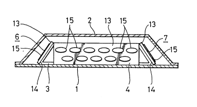
As shown in Fig. 3, the frame 3 includes a bottom
frame 8 which is fixed on the upper surfaces of the base 1
described above, and mounting frames 9 - 12 protruding
obliquely and upwardly from the bottom frame 8. And
2~379 1 1
microstrip array panels 4 - 7 are installed and fixed onto the
mounting frames 9 - 12 respectively. Further, each one of the
mounting frames 9 and lo, which is located along the
longitudinal direction of the bottom frame 8, is formed a
trapezoid, and each one of the mounting frames 11 and 12,
which is located along the traverse direction of the bottom
frame 8, is formed a triangle.
Each of the microstrip array panels 4, 5, 6 and 7,
includes a substrate 13 made of low dielectric substrate a
lo ground surface 14 formed on the reverse side of the subrate
13, and a plurality of driver elements 15 formed on the top
surface of the substrate 13 as shown in Fig. 4.
The front and rear microstrip array panels 6 and 7
are different in the panel areas and the number of driver
elements from the side microstrip array panels 4 and 5. And
these microstrip array panels are arranged as inclined in four
directions in a similar way to a roof of a house as shown in
Figs. 1 and 2.
Each of the driver elements 15 and the gland
20 surfaces 14 of microstrip array panels 4 - 7 is connected to
a distributing and coupling circuit as shown in Fig. 5.
The distributing and coupling circuit shown in the
figure includes a left distributing and coupling circuit 18,
a right distributing and coupling circuit 19, a front
distributing and coupling circuit 20, and a rear distributing
and coupling circuit 21 corresponding to the microstrip array
panels 4 - 7 respectively, and they are connected to a
transmitter/receiver, not shown in the figure, via a selecting
circuit 22.
Each of the distributing and coupling circuits
18 - 21 includes a plurality of phase shifters 23 connected
to the driver elements on one of the microstrip array panels
respectively, a distributing coupler 24 connected to the phase
shifters 23, a pre-set phase shifter 25 which adjust phase
shifts of I/0 signals in the distributing coupler 24, a change
over switch 26 connected to the pre-set phase shifter 25, and
,~ '
~ 203~
a distributing coupler 27 connected to the change over switch
26 and the selecting circuit 22. Each of the phase shifters
23 is constructed to control directivety of the antenna as a
whole by regulating the phases of I/O transmitting and
receiving signals from or to the driver elements on the
microstrip array panel. Namely, when a plurality of
transmitting signals are supplied from the distributing
couplers 24 to the phase shifters 23, the shifters regulate
the phases of the transmitting signals and supply them to the
10 driver elements 15, and regulate the phases of receiving
signals from the driver elements 15 and supply them to the
distributing couplers 24.
When transmitting signals are supplied from the pre-
set phase shifters 25 to the distributing couplers 24, the
couplers 24 distribute them to each of the phase shifters 23,
and when receiving signals are supplied from the respective
phase shifter 23 to the couplers 24, the coup]ers 24 couple
and supply them as a single receiving signal to the respective
pre-set phase shifters 25.
In this embodiment, a directional scanning is
performed from side to side as centered with respect to a
mutual rectangular direction by using the respective
microstrip antenna, and in a boundary portion between the
scanning areas of the antennas, that is, in diagonal
directions at vertical angles from the rectangle located in
the center in a plane as shown in Fig. 7, a scanning is
performed by using the adjacent antennas with each other and
combining directional characteristics of both of the adjacent
antennas.
The pre-set phase shifter 25 is constructed to
compensate a lag in phase between these antennas due to the
difference in the directions of both of these antennas.
Namely, the pre-set phase shifter 25 is constructed to
regulate phases between a microstrip array panel and the
microstrip array panel adjacent to the above one (for example
the array 6 adjacent to the array 4 or 5) such that when the
2~379~ 1
signals which are received by the respective driver elements
15 on the microstrip array panels are combined, a reduction
in the gain due to the lag in phase is prevented. When
transmitting signals are supplied from the change over switch
26 to the present phase shifter 25, the phases in the
transmitting signals are shifted and supplied to the
distributing coupler 24, and when the receiving signals are
supplied from the distributing coupler 24 the phases in the
receiving signals are shifted and supplied to the change over
10 switch 26.
The change over switch 26 includes a common terminal
26a connected to the pre-set phase shifter 25, a terminal 26b
connected to the selecting circuit 22, a terminal 26c
connected to for example the distributing coupler 27 in the
front distributing and coupling circuit 20, and a terminal 26d
connected to the distributing coupler 27 in the right
distributing and coupling circuit 19. And the common terminal
26a is connected to any one of the terminals 26b - 26d in
response to the direction of the directivity of the antenna.
Also, the distributing coupler 27 is constructed to
distribute and couple the transmitting and receiving signals
when the directivity is pointed toward the direction adjacent
to two microstrip array panels described above and to combine
and distribute the I/o signals of the array panels adjacent
to each other.
And, the selecting circuit 22 includes a common
terminal 22a connected to the transmitter/receiver, front
selecting terminals 30, 32, 34 and 36 connected to the change
over switches 26 of the left, right, front and rear
30 distributing and coupling circuits 18 - 21, and selecting
terminals 31, 33, 35 and 37 connected to the distributing
couplers 27. And the common terminal 22a is connected to any
one of the terminals 30 - 37 in response to the directivity.
Next, an operation principle and practically
specific operation of this embodiment will be described
referring to Figs. 6 to 8.
~ .
7a 203 791 1
First, in the microstrip array panels 4 - 7, as
shown in beam scanning characteristics in Fig. 6, there are
the largest gains in the directions extending to portions over
the respective driver elements 15 and smaller gains in the
directions being at right angles to those directions
(crosswise directions) as beam scanning characteristics.
Therefore, in the case where any of the microstrip
10 array panels 4 - 7 is selectively used, gains in the
directions between the neighboring microstrip array panels,
(hereinafter referred to as switching point) are reduced.
Thus, in this embodiment, for the areas in the
directions at the switching points, there are drived the two
microstrip array panels at each of the areas, for example, the
microstrip array panels 5 and 6 associated with the right and
front areas, the microstrip array panels 5 and 7 associated
with the right and rear areas, the microstrip array panels 4
and 7 associated with the left and rear area, and the
20 microstrip array panels 4 and 6 associated with the left and
front. Namely two combined antenna arrays are used and
cooperated, as shown in Fig. 8 so that a reduction in the
gains is compensated for in these areas.
As.given below, the specific operation in accordance
with the present embodiment mentioned above will be c,oncretely
described.
In the case where any one direction, for example,
a right side direction is selected so that signals are
transmitted and received in that direction, then a switch
30 within the selecting circuit 22 is so changed that the common
terminal 22a is connected to the right selecting terminal 32
-
8 203791 1
distributing and coupling circuit 19 is so changed that the
common terminal 26a is connected to the terminal 26b.
And at this time, the phases in the respective phase
shifters 23 within a right distributing and coupling
-ircuit 19 are regulated in response to the pointed
direction.
Accordingly, through the selecting circuit 22, the
change over switch 26, the pre-set phase shifter 25, the
distributing coupler 24, and the respective phase shifters
23 in the right distributing and coupling circuit 19, a
transmitter/receiver is connected to the respective driver
elements 15 on the microstrip array panel 5.
And, in the case of transmitting and receiving in the
direction at the switching point of the microstrip array
panels 5 and 6 (forward and rightward), a switch within the
selecting circuit 22 is so changed that the common terminal
22a is connected to the right front selecting terminal 33,
the switch 26 in the right distributing and coupling
circuit 19 is so changed that the common terminal 26a is
connected to the terminal 26c, and the switch 26 in the
front distributing and coupling circuit 20 is so changed
that the common terminal 26a is connected to the terminal
26d.
And at this time, the phases in the respective phase
shifters 23 within the right distributing and coupling
circuit 19 and the phases in the respective phase shifters
23 within the front distributing and coupling circuit 20
are regulated in response to a communicating direction.
Accordingly, in the case of transmitting, transmitter/
receiver input signals are supplied via the selecting
circuit 22 to the distributing coupler 27 of the right
distributing and coupling circuit 19 wherein they are
divided into two signals. And one of the divided
transmitting signals is supplied to the respective driver
elements 15 on the microstrip array panel 6 through the
- 9 - 20 3 7 9 1 1
switch 26, the pre-set phase shifters 25, the distributing
coupler 24, and the phase shifters 23 in the front
distributing and coupling circuit 20.
Also, the other transmitting signal divided by the
distributing coupler 27 in the right distributing and
coupling circuit 19 is supplied to the respective driver
elements 15 on the microstrip array panel 5 through the
switch 26, the pre-set phase shifter 25, the distributing
coupler 24 and the phase shifters 23 in the same block 19.
Thus, a radiowave is emitted from each of the driver
elements 15 on the microstrip array panels 5 and 6 and as a
result a directivity is determined by both of the
controlling phases.
And, the receiving operation in this condition is
opposite to the case of the transmitting described above.
Namely, signals received by the microstrip array panels 5
and 6 are coupled in the distributing coupler 27 in the
right distributing and coupling circuit 19 and supplied to
the transmitter/receiver (not shown in the drawing) through
the selecting circuit 22.
In this embodiment, when a beam is formed in the
direction at the switching point of the microstrip array
panels 4 - 7, two microstrip array panels associated with
this switching point are used and a lag in phase due to the
arrangement of the panels is compensated by the pre-set
phase shifter 25 so that sufficient gains can be secured
for omni directions including boundary directions of the
array panels in which very small gains have been obtained
previously.
Also, in the embodiment described above, four pre-set
phase shifters 25 are used to compensate the phases in the
transmitting and receiving signals for the microstrip array
panels 4 - 7, but a variable phase shifter may be used in
place of the pre-set phase shifter 25 to control finely
phases in response to a communicating direction so that the
most appropriate value may be obtained.
~ 2 0 3 7 9 1 1
With a view to this it will be effective to perform
control by a CPU.
INDUSTRIAL APPLICABILITY
As described above, sufficient gains can be secured
for omni directions in accordance with the present
invention, since two or more antennas adjacent to each
other cooperate to cover an area which cannot be
covered by a microstrip array antenna.